Intel is ready to begin production of MRAM memory
 So, a fundamentally new type of computer memory, called the successor of both DRAM and NAND and demonstrated at the end of last year by Samsung and Intel, begins to take on the form of a real product. At least, one more step has been taken in this direction: according to Intel, it is ready in the near future to begin production of MRAM (Magnetoresistive Random-Access Memory) on an industrial scale.
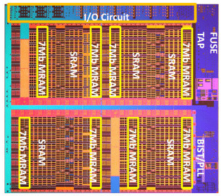
We will not dwell on the device and the principles of operation of MRAM-memory in detail - you will find a lot of detailed information at the link above. We only note its main characteristics. So, Intel uses the “write-check-write” scheme and two-stage current measurement technology in order to build perpendicular 7-MB STT-MRAM (spin-torque-transfer MRAM) arrays created using 22-nm FinFET technology.

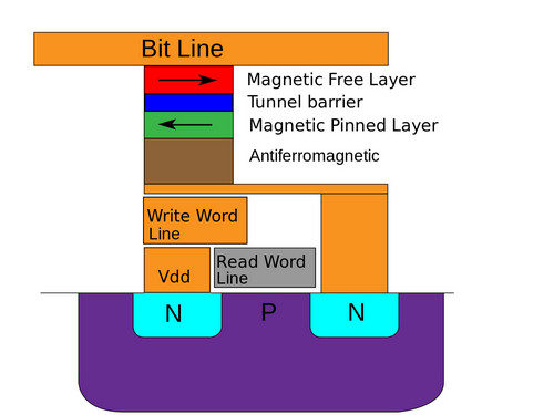
MRAM cell layout
As a non-volatile memory, MRAM arrays provide data up to 10 years at a temperature of 200 ° C, withstand up to 10 6 write cycles and up to 10 12 read cycles. In addition to high reliability, MRAM demonstrates a surprisingly good level of product yield (only 0.1% rejection), which will undoubtedly affect the cost.
We give in the plate other characteristics:
| Technology | 22FFL FinFET |
| Cell type | 1T1MTJ |
| Cell size | 0.0486 µm 2 |
| Volume | 7 Mb |
| Density (including ESA) | 10.6 Mb / mm 2 |
| Reading time | 4 ns at 0.9 V, 8 ns at 0.6 V |
| Recording time | 10 μs for the end bit |
| Overflow protection | Yes |
MRAM technology will help to overcome the reached limit of miniaturization of memory elements. In addition, MRAM can be operated in a variety of conditions, which together makes it optimal for various devices of the Internet of things. Resistive RAM (ReRAM), another type of memory Intel is currently working on, can be used as an inexpensive volatile memory for such devices . Here you can recall Optane Memory - work in this direction is also in full swing. That’s how many species you get As they say, more memory, good and different.
