Replacing analog adjustment with digital in the laboratory power supply HY3005D
The article will discuss the replacement of standard potentiometers with EC11 mechanical encoders (accumulating angle sensors) in a Mastech HY3005D power supply unit using a PIC16F1829 microcontroller and a shift register 74HC595 implementing a DAC on an R2R resistor matrix
A few years ago, I purchased a Mastech HY3005D power supply. Not so long ago there were problems with voltage regulation - the graphite coating of rheostats was worn out and setting the required voltage became a difficult task. There were no suitable rheostats, and I decided not to buy similar ones, but to change the method of adjustment.
The level of output voltage and current is set by the reference voltage supplied to the operational amplifiers. Thus, you can completely get rid of the potentiometers by replacing them with a DAC capable of delivering voltage in the desired range.
In the microchip catalog, I could not find a suitable microcontroller that has two DACs on board, and external DACs have not a small price tag and too much extra functionality. Therefore, I acquired the shift registers 74HC595 and resistors for the R2R matrix. The PIC16F1829 microcontroller was already in stock.
In order to be able to return to the original circuit, all changes are minimized - replacing the adjustment unit made on a separate board.
The circuit is based on the PIC16F1829 microcontroller operating at a frequency of 32 MHz. The clock frequency is set by the built-in clock generator, according to the datasheet it is not too accurate, but for this circuit it is not critical. The advantage of this MK is the presence of pull-up resistors on all digital inputs and two MSSP modules that implement SPI. All 18 logic pins of the microcontroller are used.
On four shift registers 74HC595and R2R matrices implemented two 16-bit DACs. The advantages of this register include the presence of a separate shift register and storage register. This allows you to write data to the register without breaking current output values. The R2R matrix is assembled on resistors with an error of 1%. It is worth noting that selective measurements showed an error of not more than 10 ohms. Initially, it was planned to use 3 registers, but when wiring the board, it seemed to me not a good solution, in addition, it was necessary to add nibbles.
The pull-up resistors built into the MC are activated at all inputs and simplify the circuit. All outputs from the encoders are connected directly to the MK terminals, a total of 4 encoders each have two outputs for the rotation sensor itself and one for the built-in button. A total of 12 conclusions MK is used to process input data. Contact bounce is smoothed with a capacity of 100nF. After changing the values of the 16-bit current and voltage buffers in accordance with the input data from the encoders, the values are transferred to the shift registers 74HC595 via SPI. To reduce data transfer time, two SPI modules are used, which allows data to be transmitted simultaneously for current and voltage. After the data is transferred to the register, a command is sent to transfer data from the shift buffer to the storage buffer. The outputs of the register are connected to the matrix R2R acting as a divider for the DAC.
The buttons built into the encoders set the minimum (encoder button for smooth adjustment) or maximum (encoder button for coarse adjustment), respectively, for current or voltage.
On the Internet, I did not find a scheme that completely coincided with mine, so I took the first link. Made corrections on the revealed inconsistencies and then added the changes. I drew a diagram of the adjustment block in TinyCAD - download the file HY3005D-regulator.dsn .
The final scheme after refinement The
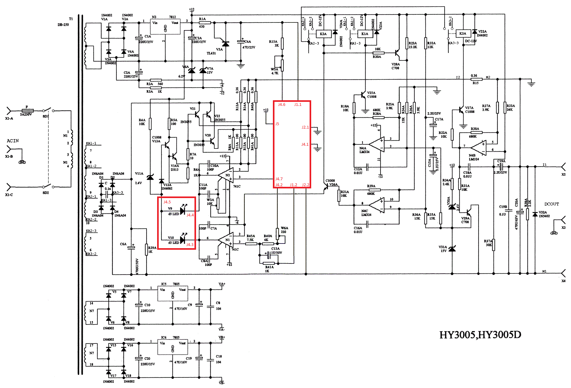
portable unit with adjustment (highlighted in red) was placed in a separate scheme.

A digital voltmeter with a display on the front panel (it is not on the diagrams) is connected to the J3 connector.
Below is a list of components used (the case is indicated in parentheses). All were purchased at different times in China. It is important to use LEDs with the same characteristics as native ones, as they stand in series in the output circuit of operational amplifiers (I took the same ones that stood on my motherboard).
I bred the board in Sprint Layout 6 - download the file HY3005D-regulator.lay6 . Unfortunately, the original on which I made my version was not preserved, in lay6 format already with corrections identified during the assembly:
Made using film photoresist. I suffered for a long time with a small wiring of registers. In the latter version, there were small flaws that had to be cleaned after etching. But in general, the board failed. There are still not enough two jumpers to connect the ground on the front and back sides.
As you can see, the changes are minimal, all the old connectors remained unchanged. I had to add food separately, because the only voltage coming to the 2.5V adjustment board is not suitable for the native divider. If you remove the zener diode to 2.5V (V5A) on the main board of the power supply unit and put a jumper in the place of the resistor (R1A), you can do without additional supply of 12V power.
C code for the XC8 compiler. Stitched the original PICkit 3.
For the minimum values, VoltageMin and CurrentMin are set to 1, because at 0 in the buffer, the adjustment stops working until I understand where the problem is. Rates * Rate * selected multiple and most convenient in my opinion. For the SendData method, I did not pass variables as parameters to save machine instructions and memory. Low Voltage Firmware (LVP) mode must be turned off, otherwise RA3 will not work as a digital input. Interrupts are not used, the tc_int method is present in the code so that the compiler places the main block at the beginning of the ROM.
For firmware, it is enough to remove the jumpers, connect the PICkit 3 (or another programmer) and perform the firmware. In the first version there were no jumpers on the CLK and DAT, so I had to unsolder the smoothing capacitors, flash them and then solder them back.
UPD:After installing additional capacities on the power line, the problem of exiting the counter from the zero position disappeared. I also had to change the direction of rotation. Apparently, the noise from the AMS1117 rectifier prevented the correct recognition of the state of the encoders. Additionally, I added a setting of starting values, now the default voltage is set to 5 volts (the current is still at maximum). Before the first data sending, a delay of 50ms was inserted into the registers (the delay value was taken with a large margin) to wait for the SPI modules to initialize.
After the final assembly of the device, a voltage measurement was performed between the contacts J4.1 - J4.2 (voltage regulation) and J4.1 - J4.7 (current regulation). According to the data obtained, graphs (below under the spoiler) of the value / voltage dependencies for the DAC are plotted.
The calculated values of the voltages are obtained by the formula (U * D) / (2 ^ K), where
U is the voltage at the output of the register, taking into account the dividers in the main circuit (for current DACs - 4950mV, for voltage DACs - 3550mV);
D is the decimal value of the DAC counter;
K - DAC bit depth (16 bit)
Foreword
A few years ago, I purchased a Mastech HY3005D power supply. Not so long ago there were problems with voltage regulation - the graphite coating of rheostats was worn out and setting the required voltage became a difficult task. There were no suitable rheostats, and I decided not to buy similar ones, but to change the method of adjustment.
The level of output voltage and current is set by the reference voltage supplied to the operational amplifiers. Thus, you can completely get rid of the potentiometers by replacing them with a DAC capable of delivering voltage in the desired range.
In the microchip catalog, I could not find a suitable microcontroller that has two DACs on board, and external DACs have not a small price tag and too much extra functionality. Therefore, I acquired the shift registers 74HC595 and resistors for the R2R matrix. The PIC16F1829 microcontroller was already in stock.
In order to be able to return to the original circuit, all changes are minimized - replacing the adjustment unit made on a separate board.
Description of work
The circuit is based on the PIC16F1829 microcontroller operating at a frequency of 32 MHz. The clock frequency is set by the built-in clock generator, according to the datasheet it is not too accurate, but for this circuit it is not critical. The advantage of this MK is the presence of pull-up resistors on all digital inputs and two MSSP modules that implement SPI. All 18 logic pins of the microcontroller are used.
On four shift registers 74HC595and R2R matrices implemented two 16-bit DACs. The advantages of this register include the presence of a separate shift register and storage register. This allows you to write data to the register without breaking current output values. The R2R matrix is assembled on resistors with an error of 1%. It is worth noting that selective measurements showed an error of not more than 10 ohms. Initially, it was planned to use 3 registers, but when wiring the board, it seemed to me not a good solution, in addition, it was necessary to add nibbles.
The pull-up resistors built into the MC are activated at all inputs and simplify the circuit. All outputs from the encoders are connected directly to the MK terminals, a total of 4 encoders each have two outputs for the rotation sensor itself and one for the built-in button. A total of 12 conclusions MK is used to process input data. Contact bounce is smoothed with a capacity of 100nF. After changing the values of the 16-bit current and voltage buffers in accordance with the input data from the encoders, the values are transferred to the shift registers 74HC595 via SPI. To reduce data transfer time, two SPI modules are used, which allows data to be transmitted simultaneously for current and voltage. After the data is transferred to the register, a command is sent to transfer data from the shift buffer to the storage buffer. The outputs of the register are connected to the matrix R2R acting as a divider for the DAC.
The buttons built into the encoders set the minimum (encoder button for smooth adjustment) or maximum (encoder button for coarse adjustment), respectively, for current or voltage.
Scheme
On the Internet, I did not find a scheme that completely coincided with mine, so I took the first link. Made corrections on the revealed inconsistencies and then added the changes. I drew a diagram of the adjustment block in TinyCAD - download the file HY3005D-regulator.dsn .
Original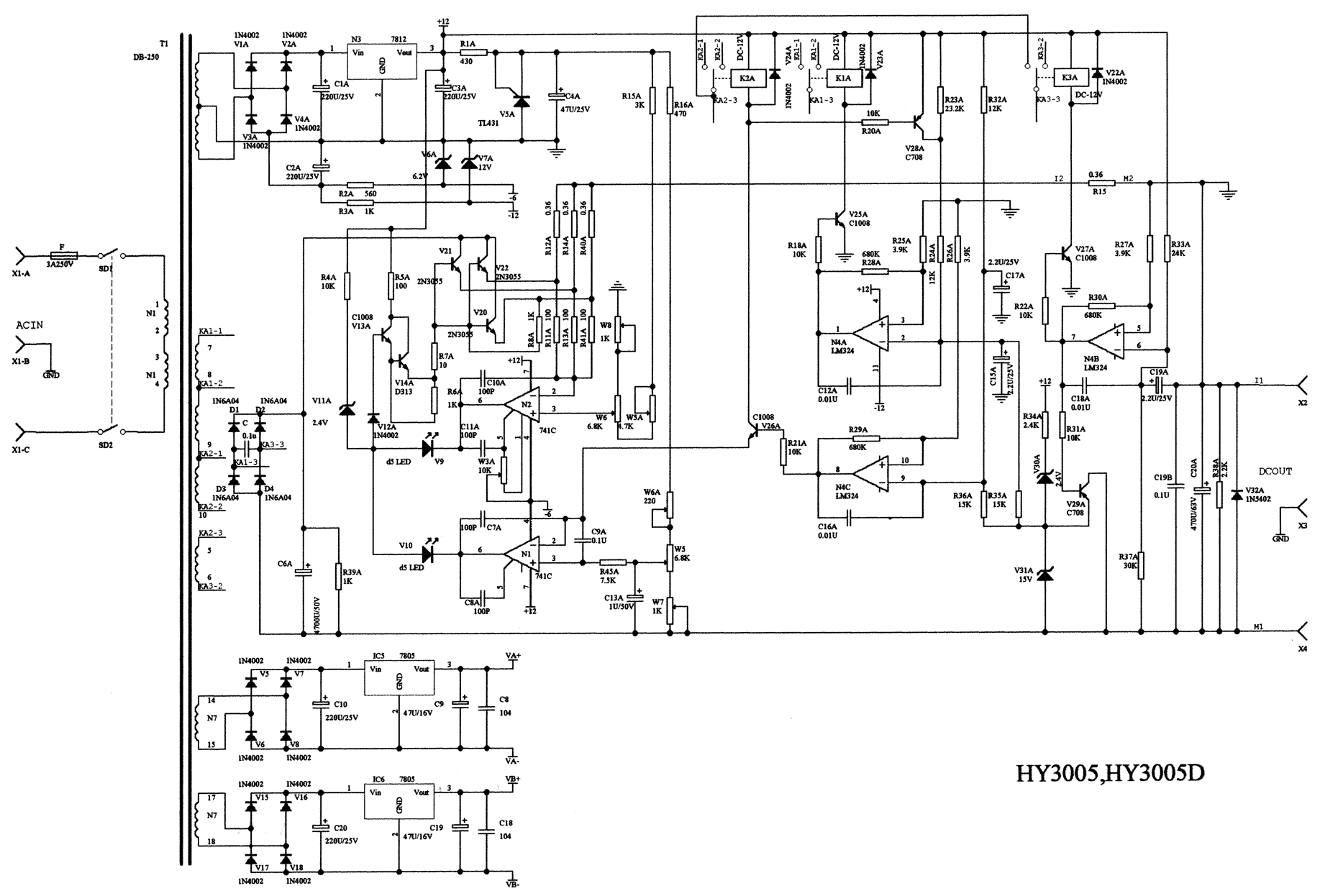
After found inaccuracies
The final scheme after refinement The
portable unit with adjustment (highlighted in red) was placed in a separate scheme.
A digital voltmeter with a display on the front panel (it is not on the diagrams) is connected to the J3 connector.
Components Used
Below is a list of components used (the case is indicated in parentheses). All were purchased at different times in China. It is important to use LEDs with the same characteristics as native ones, as they stand in series in the output circuit of operational amplifiers (I took the same ones that stood on my motherboard).
- U1: PIC16F1829I / ML microcontroller (QFN)
- U2 - U5: shift register 74HC595BQ (DHVQFN16 or SOT-763)
- U6: AMS1117 5V linear voltage regulator (SOT-223)
- RE1 - RE4: mechanical accumulating angle sensor EC11
- R1, R2 and R2R matrices: 1 and 2 kΩ resistors (SMD 0402)
- C1 - C12, C14-C17: Ceramic Capacitors GRM21BR71E104KA01L 100nF (SMD 0805)
- C13: tantalum capacitor 22mkF 16V (tiv B)
- D1, D2: front panel voltage / current LEDs
Pay
I bred the board in Sprint Layout 6 - download the file HY3005D-regulator.lay6 . Unfortunately, the original on which I made my version was not preserved, in lay6 format already with corrections identified during the assembly:
- I added jumpers next to the firmware interface to the interrupt connection of the smooth current control encoder, because capacities filtering contact bounce prevented flashing the controller
- Added missing jumpers for ground between the sides
- Moved the 5V stabilizing assembly to the other side to reduce through jumpers
- Added smoothing capacitors on the power line ( discussion )
Photo after etching and drilling (first version)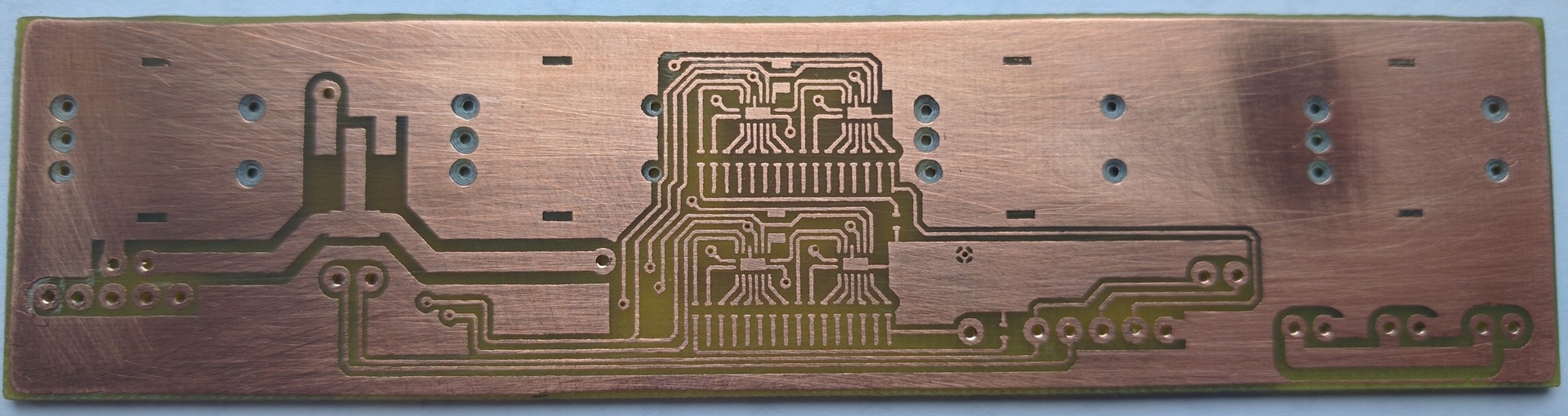

Made using film photoresist. I suffered for a long time with a small wiring of registers. In the latter version, there were small flaws that had to be cleaned after etching. But in general, the board failed. There are still not enough two jumpers to connect the ground on the front and back sides.
After entering the identified problems (second version)

Three jumpers with a nominal value of 0 ohms in the SMD 0805 package are used as jumpers.
Three jumpers with a nominal value of 0 ohms in the SMD 0805 package are used as jumpers.
Photo after unsoldering and installation in place
On the left side is the power supply itself. In the right - the front panel face down. Green wire from upper left to lower right - additional 12V power.
On the left side is the power supply itself. In the right - the front panel face down. Green wire from upper left to lower right - additional 12V power.
As you can see, the changes are minimal, all the old connectors remained unchanged. I had to add food separately, because the only voltage coming to the 2.5V adjustment board is not suitable for the native divider. If you remove the zener diode to 2.5V (V5A) on the main board of the power supply unit and put a jumper in the place of the resistor (R1A), you can do without additional supply of 12V power.
Firmware
C code for the XC8 compiler. Stitched the original PICkit 3.
config.h
// PIC16F1829 Configuration Bit Settings
// 'C' source line config statements
#include
// #pragma config statements should precede project file includes.
// Use project enums instead of #define for ON and OFF.
// CONFIG1
#pragma config FOSC = INTOSC    // Oscillator Selection (INTOSC oscillator: I/O function on CLKIN pin)
#pragma config WDTE = OFF       // Watchdog Timer Enable (WDT disabled)
#pragma config PWRTE = OFF      // Power-up Timer Enable (PWRT disabled)
#pragma config MCLRE = OFF      // MCLR Pin Function Select (MCLR/VPP pin function is digital input)
#pragma config CP = OFF         // Flash Program Memory Code Protection (Program memory code protection is disabled)
#pragma config CPD = OFF        // Data Memory Code Protection (Data memory code protection is disabled)
#pragma config BOREN = OFF      // Brown-out Reset Enable (Brown-out Reset disabled)
#pragma config CLKOUTEN = OFF   // Clock Out Enable (CLKOUT function is disabled. I/O or oscillator function on the CLKOUT pin)
#pragma config IESO = OFF       // Internal/External Switchover (Internal/External Switchover mode is disabled)
#pragma config FCMEN = OFF      // Fail-Safe Clock Monitor Enable (Fail-Safe Clock Monitor is disabled)
// CONFIG2
#pragma config WRT = OFF        // Flash Memory Self-Write Protection (Write protection off)
#pragma config PLLEN = OFF      // PLL Enable (4x PLL disabled)
#pragma config STVREN = ON      // Stack Overflow/Underflow Reset Enable (Stack Overflow or Underflow will cause a Reset)
#pragma config BORV = LO        // Brown-out Reset Voltage Selection (Brown-out Reset Voltage (Vbor), low trip point selected.)
#pragma config LVP = OFF        // Low-Voltage Programming Enable (High-voltage on MCLR/VPP must be used for programming)
main.c
#include "config.h"
#define _XTAL_FREQ 32000000
#pragma intrinsic(_delay)
extern void _delay(unsigned long);
#define __delay_us(x) _delay((unsigned long)((x)*(_XTAL_FREQ/4000000.0)))
#define __delay_ms(x) _delay((unsigned long)((x)*(_XTAL_FREQ/4000.0)))
#define TransferNotDone          !(SSP2STAT&0b00000001)
#define StoreAll                 LATA4
#define ResetAll                 LATC6
#define VoltageSharpCHA          RC1
#define VoltageSharpCHB          RC0
#define VoltageSharpBTN          RA2
#define VoltageSmoothCHA         RB5
#define VoltageSmoothCHB         RB4
#define VoltageSmoothBTN         RC2
#define CurrentSharpCHA          RC5
#define CurrentSharpCHB          RC4
#define CurrentSharpBTN          RC3
#define CurrentSmoothCHA         RA1
#define CurrentSmoothCHB         RA0
#define CurrentSmoothBTN         RA3
#define VoltageRateSharp         0x0100
#define VoltageRateSmooth        0x0010
#define CurrentRateSharp         0x0040
#define CurrentRateSmooth        0x0004
#define VoltageMax               0xC000
#define CurrentMax               0x5000
#define VoltageMin               0x0000
#define CurrentMin               0x0000
#define VoltageStart             0x1E00
#define CurrentStart             CurrentMax
unsigned short VoltageBuff;
unsigned short CurrentBuff;
void interrupt tc_int() {
};
void SendData() {
    SSP1BUF = VoltageBuff>>8;
    SSP2BUF = CurrentBuff>>8;
    while ( TransferNotDone );
    SSP1BUF = VoltageBuff;
    SSP2BUF = CurrentBuff;
    while ( TransferNotDone );
    StoreAll = 1;
    StoreAll = 0;
};
void main() {
    // Configure oscillator for 32MHz
    //             76543210
    OSCCON     = 0b11110000; //B1
    // Enable individual pull-ups
    //             76543210
    OPTION_REG = 0b01111111; //B1
    // Configure analog port (1 - enable, 0 - disable)
    //             76543210
    ANSELA     = 0b00000000; //B3
    ANSELB     = 0b00000000; //B3
    ANSELC     = 0b00000000; //B3
    // Reset latch
    //             76543210
    LATA       = 0b00000000; //B2
    LATB       = 0b00000000; //B2
    LATC       = 0b00000000; //B2
    // Alternate pin function (set SDO2 on RA5)
    //             76543210
    APFCON0    = 0b00000000; //B2
    APFCON1    = 0b00100000; //B2
    // Configure digital port (1 - input, 0 - output)
    //             76543210
    TRISA      = 0b00001111; //B1
    TRISB      = 0b00110000; //B1
    TRISC      = 0b00111111; //B1
    // Configure input level (1 - CMOS, 0 - TTL)
    INLVLA     = 0b11000000; //B7
    INLVLB     = 0b00001111; //B7
    INLVLC     = 0b00000000; //B7
    // Configure individual pull-ups (1 - enable, 0 - disable)
    //             76543210
    WPUA       = 0b00111111; //B4
    WPUB       = 0b11110000; //B4
    WPUC       = 0b11111111; //B4
    ResetAll = 0;
    ResetAll = 1;
    // Configure SPI in master mode
    //             76543210
  //SSP1ADD    = 0b00000000; //B4
    SSP1STAT   = 0b01000000; //B4
    SSP1CON3   = 0b00000000; //B4
    SSP1CON1   = 0b00100000; //B4
  //SSP1ADD    = 0b00000000; //B4
    SSP2STAT   = 0b01000000; //B4
    SSP2CON3   = 0b00000000; //B4
    SSP2CON1   = 0b00100000; //B4
    VoltageBuff = VoltageStart;
    CurrentBuff = CurrentStart;
    __delay_ms(50);
    SendData();
    while ( 1 ) {
        if ( !VoltageSharpCHA ) {
            if ( VoltageSharpCHB ) { VoltageBuff-=VoltageRateSharp; if ( VoltageBuff > VoltageMax ) VoltageBuff = VoltageMin; }
                              else { VoltageBuff+=VoltageRateSharp; if ( VoltageBuff > VoltageMax ) VoltageBuff = VoltageMax; }
            while ( !VoltageSharpCHA );
            SendData();
        }
        if ( !VoltageSmoothCHA ) {
            if ( VoltageSmoothCHB ) { VoltageBuff-=VoltageRateSmooth; if ( VoltageBuff > VoltageMax ) VoltageBuff = VoltageMin; }
                               else { VoltageBuff+=VoltageRateSmooth; if ( VoltageBuff > VoltageMax ) VoltageBuff = VoltageMax; }
            while ( !VoltageSmoothCHA );
            SendData();
        }
        if ( !CurrentSharpCHA ) {
            if ( CurrentSharpCHB ) { CurrentBuff-=CurrentRateSharp; if ( CurrentBuff > CurrentMax ) CurrentBuff = CurrentMin; }
                              else { CurrentBuff+=CurrentRateSharp; if ( CurrentBuff > CurrentMax ) CurrentBuff = CurrentMax; }
            while ( !CurrentSharpCHA );
            SendData();
        }
        if ( !CurrentSmoothCHA ) {
            if ( CurrentSmoothCHB ) { CurrentBuff-=CurrentRateSmooth; if ( CurrentBuff > CurrentMax ) CurrentBuff = CurrentMin; }
                               else { CurrentBuff+=CurrentRateSmooth; if ( CurrentBuff > CurrentMax ) CurrentBuff = CurrentMax; }
            while ( !CurrentSmoothCHA );
            SendData();
        }
        if ( !VoltageSharpBTN  ) { VoltageBuff = VoltageMax; while ( !VoltageSharpBTN  ); SendData(); }
        if ( !VoltageSmoothBTN ) { VoltageBuff = VoltageMin; while ( !VoltageSmoothBTN ); SendData(); }
        if ( !CurrentSharpBTN  ) { CurrentBuff = CurrentMax; while ( !CurrentSharpBTN  ); SendData(); }
        if ( !CurrentSmoothBTN ) { CurrentBuff = CurrentMin; while ( !CurrentSmoothBTN ); SendData(); }
    };
}
For the minimum values, VoltageMin and CurrentMin are set to 1, because at 0 in the buffer, the adjustment stops working until I understand where the problem is. Rates * Rate * selected multiple and most convenient in my opinion. For the SendData method, I did not pass variables as parameters to save machine instructions and memory. Low Voltage Firmware (LVP) mode must be turned off, otherwise RA3 will not work as a digital input. Interrupts are not used, the tc_int method is present in the code so that the compiler places the main block at the beginning of the ROM.
For firmware, it is enough to remove the jumpers, connect the PICkit 3 (or another programmer) and perform the firmware. In the first version there were no jumpers on the CLK and DAT, so I had to unsolder the smoothing capacitors, flash them and then solder them back.
UPD:After installing additional capacities on the power line, the problem of exiting the counter from the zero position disappeared. I also had to change the direction of rotation. Apparently, the noise from the AMS1117 rectifier prevented the correct recognition of the state of the encoders. Additionally, I added a setting of starting values, now the default voltage is set to 5 volts (the current is still at maximum). Before the first data sending, a delay of 50ms was inserted into the registers (the delay value was taken with a large margin) to wait for the SPI modules to initialize.
Output voltage characteristics
After the final assembly of the device, a voltage measurement was performed between the contacts J4.1 - J4.2 (voltage regulation) and J4.1 - J4.7 (current regulation). According to the data obtained, graphs (below under the spoiler) of the value / voltage dependencies for the DAC are plotted.
Graphs

The calculated values of the voltages are obtained by the formula (U * D) / (2 ^ K), where
U is the voltage at the output of the register, taking into account the dividers in the main circuit (for current DACs - 4950mV, for voltage DACs - 3550mV);
D is the decimal value of the DAC counter;
K - DAC bit depth (16 bit)
What can be improved
- add timer values saving
- tie the standard values to the encoder buttons, for example, for voltage: 3.3; 5.0; 7.5; 12V
- to protect against an unknown value at startup, it is better to connect MR to 1, and pull the OE through the resistor to 1 and reset to 0 after initializing the MK.
- replace the DAC with a PWM with a smoothing chain ( LampTester suggested here )