Expert opinion: Analysis of the properties of nanomaterials using an electron microscope
NITU "MISiS" annually hosts the event "Christmas Lectures" . As part of this event, our leading scientists give a lecture on their research areas and major achievements. This year, our leading scientist, Director of the Nanotube Center of the National Institute of Materials Science, Tsukuba, Professor of Tsukuba University, Japan, Scientific Director of the Inorganic Nanomaterials Research Laboratory of NUST MISIS, D.V. opened the traditional Christmas lecture cycle . Golberg . He currently has one of the highest Hirsch indices (80)
In his lecture, he talked about the analysis of the properties of nanomaterials using an electron microscope. It is also important to note that in his lecture D.V. Golberg demonstrated a study that has no analogues in the world, part of his presentation contains unique material, which, unfortunately, has not yet been authorized for publication. We turned to him to write thesis about his lecture within the framework of our traditional cycle of publications in the form of expert opinion. He also agreed to answer readers' questions, if any. After the lecture, Dmitry Viktorovich flew to the United States and wrote a publication for us literally from an airplane. The format, unfortunately, is not popular science, and we are not entitled to set the scope for writing a note for a scientist, since it was originally planned that he would write for our discussion science clubwhere the target audience are engineers of specialized specialties. But, since a scientist of this level doesn’t write so often for popular science publications, we would still like to publish this material in our corporate blog on GT. This can not be considered a note from the series "I just leave it here", for specialists this material will really seem very exciting and interesting.

Understanding the mechanical, electrical, and optoelectronic properties of nanomaterials, in particular, at a specific structural level, is of key importance due to the interest in integrating them into modern technologies. Nevertheless, in the vast majority of cases, measurements of such properties are carried out using instruments that do not have direct access to the atomic structures of nanomaterials, their crystallography, and spatially resolved chemical composition. This fact significantly limits the relevance of the data collected, since all the specific structural features of nanometric objects before / during / after testing are usually hidden. In view of the foregoing, the results obtained cannot be directly related to a specific nanostructure, its internal morphology, and defects. Thus, a large scatter of data of a mechanical, electrical, and optoelectronic nature is a common feature of various scientific groups and their publications. Until now, this drawback has greatly complicated the work of practical engineers and technologists and has led to numerous uncertainties regarding the real production potentials of nanomaterials.
In this publication, I will demonstrate the benefits of the recently developed within our group in Tsukuba and advanced in situ transmission electron microscopy (TEM) technique for analyzing the mechanical, electrical, and optoelectronic properties of various inorganic nanostructures [1-3]. Elasticity, ductility, strength, electrical resistance, conductivity, temperature difference, photocurrent, photovoltage and spatially resolved cathodoluminescence maps can be analyzed by a high resolution transmission electron microscope (PEMVR) using piezoelectric controlled nanomanipulators and / or optical fibers placed in TEM holders.
The general scheme of the device used in our experiments is shown in Figure 1. A pre-located nano-sample can be charged, bent or stretched, and also illuminated with light of different intensities, wavelengths, or pulse frequencies. All types of holders (Manufacturer Nanofactory Instruments AB, Sweden) were compatible with the JEOL JEM-3100FEF PEMVR microscope (Omega filter) with a spatial resolution of 0.17 nm. The microscope operating at 300 kV has an X-ray dispersion detector (EDX) and the possibility of electron energy loss spectroscopy for chemical analysis with spatial resolution and the creation of element maps of the tested nanomaterials before / during and after measurements.
The precise placement of the nanosample in the holders is the first step towards reliable and reproducible recording of data and properties. Freshly cut flat gold wire (250 microns in the initial diameter) is first immersed in particles of nanomaterials ground to a powder state. Then the gold wire with attached nanomaterial is mounted on a fixed or movable holder. It should be noted that nano-objects are usually attracted to the gold wire as a result of simple physical adhesion; Only in some cases was silver paste used to improve physical contact between the sample and the gold electrode. The holders can be STM-TEM type and non-conductive or conductive AFM-TEM type (cantilevers made of silicon coated with ~ 15 nm Pt). Also, optical fibers could be connected to external light sources.
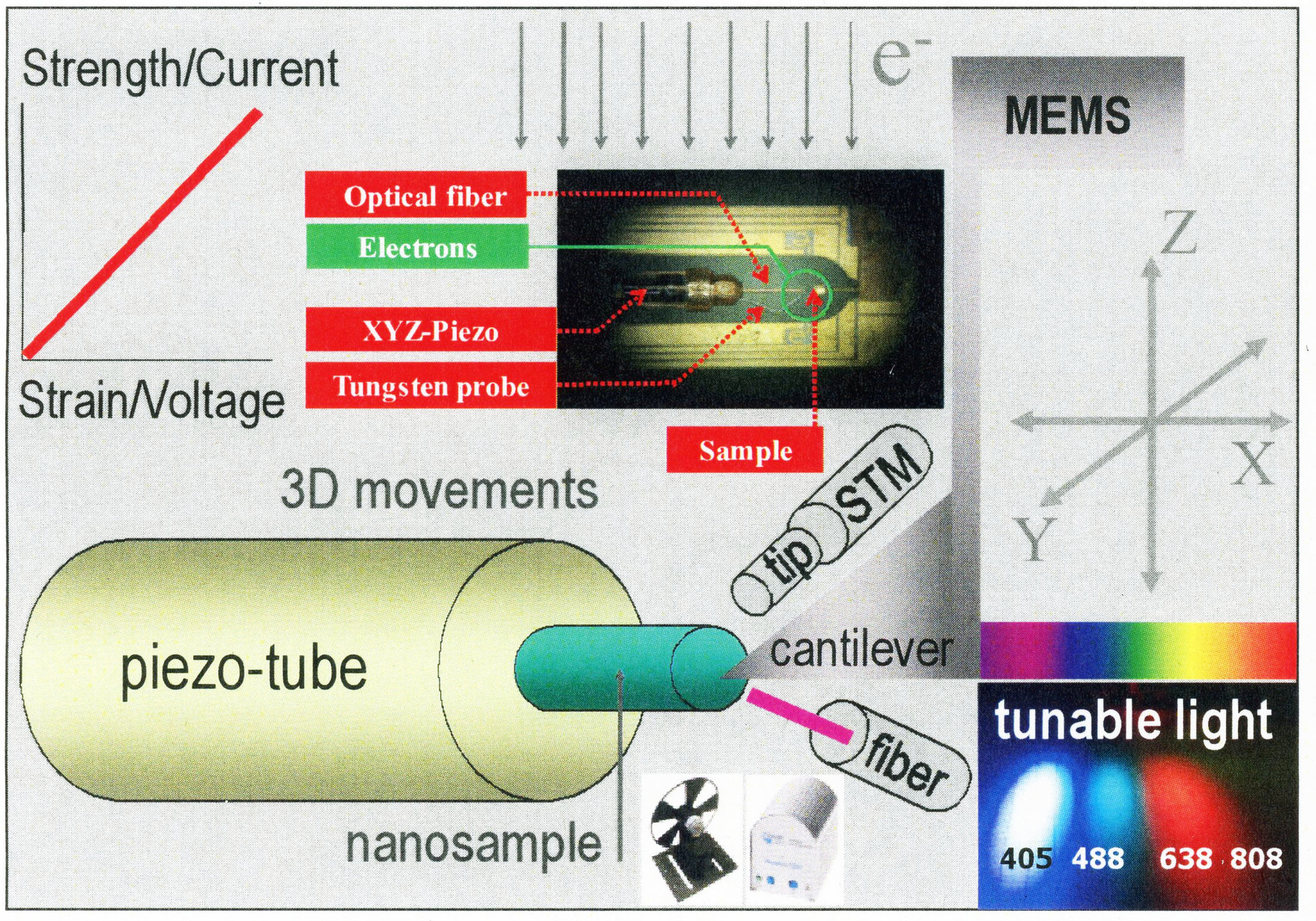
Figure 1. General scheme of a JEOL JEM-3100FEF electron microscope (Omega filter) with TEM capabilities for studying nanosamples using a CTM tip, AFM cantilever, as well as light with different intensities, wavelengths, or pulse frequencies in tandem with their bend for measuring optical electronic or photoelectric properties.
Then, using piezo-motor manipulations in PEMVR, the relative positions of the wire with the placed nanomaterial samples and the STM tip, or AFM cantilevers, or optical fiber, were precisely adjusted in three dimensions X, Y and Z, inside the pole end of the microscope with an accuracy of more than 1 nm Finally, the relative heights of the two terminal holders are accurately fixed using the TEM oscillation function. After this, close physical contact can be achieved between the studied nanoobject and the tip of the STM or AFM cantilever. In addition, the optical fiber can be moved as close to the sample as possible to minimize light scattering inside the TEM column. For the STM-TEM STM system, the tip (or a wire sample, depending on the polarity scheme) can be charged up to ± 140 V. The force measurement by the AFM TEM cantilever can be carried out using the MEMS sensor located in its lower part. Before measurements, the cantilever constants were calculated and the mV-LV voltage coefficients of the MEMS sensors were calibrated using preliminary indentation of the metal wire. Laser diodes with fixed wavelengths, for example 405, 488, 638, and 808 nm, or a bright wide powerful emitting light source connected to a monochromator and chopper were used for optoelectronic and photoelectric tests.
Using the complex device considered above, we were able to measure and analyze for the first time bending strength and tensile strength, Young's modulus and fracture toughness of various 1D multilayer and single-layer carbon nanotubes, boron nitride and dichalcogenide nanotubes, silicon nanowires, boron and gallium nitride, and various 2D nanosheets and graphene-like nanostructures. Particular attention was paid to illustrating the specific kinetics of deformation at the nanoscale. These first results were obtained with direct bending or tension using the AFM-TEM apparatus [1.4–7]. An increase in temperature at a given point of nanomaterials to ~ 2000 ° C or more when heated by electric current in the STM-TEM holder allowed us to shed light on existing temperature gradients, thermal resistance, intra-diffusion phenomena and the kinetics of amorphization / crystallization of nanoscale metals in nanospace [8,9]. Peeling of individual atomic layers of dichalcogenide (MoS2) to one layer from a single crystal was carried out in TEMP with full control of energy, distribution of stress and strain fields at the visualization level with atomic resolution [10]. Thus, the open process simulates the most popular micromechanical separation of nanosheets from graphene-like materials and provides important tips for practical development, physical understanding and optimization of this method. Most importantly, the main quantity - the surface energy of the atomic layers of MoS2 - was determined to be 0.11 N / m. Finally, under TEM conditions, optoelectronic and photoelectric experiments on titanium oxide nanoparticles, zinc oxide nanowires,
The developed and performed mechanical and optoelectronic tests in the HRTEM allowed to shed additional light on the true relationship between the structure and properties of many complex nanomaterials, such as various inorganic nanotubes, nanowires, nanosheets and nanoparticles, which is the Holy Grail of Material Science.
In his lecture, he talked about the analysis of the properties of nanomaterials using an electron microscope. It is also important to note that in his lecture D.V. Golberg demonstrated a study that has no analogues in the world, part of his presentation contains unique material, which, unfortunately, has not yet been authorized for publication. We turned to him to write thesis about his lecture within the framework of our traditional cycle of publications in the form of expert opinion. He also agreed to answer readers' questions, if any. After the lecture, Dmitry Viktorovich flew to the United States and wrote a publication for us literally from an airplane. The format, unfortunately, is not popular science, and we are not entitled to set the scope for writing a note for a scientist, since it was originally planned that he would write for our discussion science clubwhere the target audience are engineers of specialized specialties. But, since a scientist of this level doesn’t write so often for popular science publications, we would still like to publish this material in our corporate blog on GT. This can not be considered a note from the series "I just leave it here", for specialists this material will really seem very exciting and interesting.
Photography / Brodskaya Maria press service of NUST “MISiS” - Christmas lecture by D.V. Golberg at NUST “MISiS”
 | Dmitry Viktorovich Golberg, Professor, Tsukuba University, Japan Scientific Director of the Research Laboratory "Inorganic Nanomaterials" NUST "MISiS" |
In this publication, I will demonstrate the benefits of the recently developed within our group in Tsukuba and advanced in situ transmission electron microscopy (TEM) technique for analyzing the mechanical, electrical, and optoelectronic properties of various inorganic nanostructures [1-3]. Elasticity, ductility, strength, electrical resistance, conductivity, temperature difference, photocurrent, photovoltage and spatially resolved cathodoluminescence maps can be analyzed by a high resolution transmission electron microscope (PEMVR) using piezoelectric controlled nanomanipulators and / or optical fibers placed in TEM holders.
The general scheme of the device used in our experiments is shown in Figure 1. A pre-located nano-sample can be charged, bent or stretched, and also illuminated with light of different intensities, wavelengths, or pulse frequencies. All types of holders (Manufacturer Nanofactory Instruments AB, Sweden) were compatible with the JEOL JEM-3100FEF PEMVR microscope (Omega filter) with a spatial resolution of 0.17 nm. The microscope operating at 300 kV has an X-ray dispersion detector (EDX) and the possibility of electron energy loss spectroscopy for chemical analysis with spatial resolution and the creation of element maps of the tested nanomaterials before / during and after measurements.
The precise placement of the nanosample in the holders is the first step towards reliable and reproducible recording of data and properties. Freshly cut flat gold wire (250 microns in the initial diameter) is first immersed in particles of nanomaterials ground to a powder state. Then the gold wire with attached nanomaterial is mounted on a fixed or movable holder. It should be noted that nano-objects are usually attracted to the gold wire as a result of simple physical adhesion; Only in some cases was silver paste used to improve physical contact between the sample and the gold electrode. The holders can be STM-TEM type and non-conductive or conductive AFM-TEM type (cantilevers made of silicon coated with ~ 15 nm Pt). Also, optical fibers could be connected to external light sources.
Figure 1. General scheme of a JEOL JEM-3100FEF electron microscope (Omega filter) with TEM capabilities for studying nanosamples using a CTM tip, AFM cantilever, as well as light with different intensities, wavelengths, or pulse frequencies in tandem with their bend for measuring optical electronic or photoelectric properties.
Then, using piezo-motor manipulations in PEMVR, the relative positions of the wire with the placed nanomaterial samples and the STM tip, or AFM cantilevers, or optical fiber, were precisely adjusted in three dimensions X, Y and Z, inside the pole end of the microscope with an accuracy of more than 1 nm Finally, the relative heights of the two terminal holders are accurately fixed using the TEM oscillation function. After this, close physical contact can be achieved between the studied nanoobject and the tip of the STM or AFM cantilever. In addition, the optical fiber can be moved as close to the sample as possible to minimize light scattering inside the TEM column. For the STM-TEM STM system, the tip (or a wire sample, depending on the polarity scheme) can be charged up to ± 140 V. The force measurement by the AFM TEM cantilever can be carried out using the MEMS sensor located in its lower part. Before measurements, the cantilever constants were calculated and the mV-LV voltage coefficients of the MEMS sensors were calibrated using preliminary indentation of the metal wire. Laser diodes with fixed wavelengths, for example 405, 488, 638, and 808 nm, or a bright wide powerful emitting light source connected to a monochromator and chopper were used for optoelectronic and photoelectric tests.
Using the complex device considered above, we were able to measure and analyze for the first time bending strength and tensile strength, Young's modulus and fracture toughness of various 1D multilayer and single-layer carbon nanotubes, boron nitride and dichalcogenide nanotubes, silicon nanowires, boron and gallium nitride, and various 2D nanosheets and graphene-like nanostructures. Particular attention was paid to illustrating the specific kinetics of deformation at the nanoscale. These first results were obtained with direct bending or tension using the AFM-TEM apparatus [1.4–7]. An increase in temperature at a given point of nanomaterials to ~ 2000 ° C or more when heated by electric current in the STM-TEM holder allowed us to shed light on existing temperature gradients, thermal resistance, intra-diffusion phenomena and the kinetics of amorphization / crystallization of nanoscale metals in nanospace [8,9]. Peeling of individual atomic layers of dichalcogenide (MoS2) to one layer from a single crystal was carried out in TEMP with full control of energy, distribution of stress and strain fields at the visualization level with atomic resolution [10]. Thus, the open process simulates the most popular micromechanical separation of nanosheets from graphene-like materials and provides important tips for practical development, physical understanding and optimization of this method. Most importantly, the main quantity - the surface energy of the atomic layers of MoS2 - was determined to be 0.11 N / m. Finally, under TEM conditions, optoelectronic and photoelectric experiments on titanium oxide nanoparticles, zinc oxide nanowires,
The developed and performed mechanical and optoelectronic tests in the HRTEM allowed to shed additional light on the true relationship between the structure and properties of many complex nanomaterials, such as various inorganic nanotubes, nanowires, nanosheets and nanoparticles, which is the Holy Grail of Material Science.
Sources:
[1] Golberg D. et al. Nano Lett. 7, 2146 (2007).
[2] Golberg D. et al. Adv. Mater. 19, 1937 (2007).
[3] Golberg D.et al. Adv. Mater. 24, 177 (2012).
[4] Wang MS, Golberg D. et al. Adv. Mater. 22, 4071 (2010).
[5] Wei XL, Wang MS, Bando Y., Golberg D. Adv. Mater. 22, 4895 (2010).
[6] Tang DM, Golberg D. et al. Nano Lett. 12, 1898 (2012).
[7] Wei XL, Xiao S., Li F., Tang DM, Chen Q., Bando Y., Golberg D. Nano Lett. 15, 689 (2015).
[8] Costa PMFJ, Gautam UK, Bando Y., Golberg D. Nature Commun. 2, 4121 (2011).
[9] Tang DM, Golberg D. et al. Nano Lett. (2015), submitted for publication.
[10] Tang DM, Golberg D. et al. Nature Commun. 5, 3631 (2014).
[11] Zhang C., Golberg D. et al. Nanotechnology26, 154001 (2015).
[12] Zhang C., Xu Z., Golberg D. et al. Appl. Phys. Lett. 107, 051735 (2015).