Launching Bare-metal applications on Cyclone V SoC
Introduction
For some people, the FPGA SoC is something inaccessible to understanding, and this article should correct this misunderstanding. We will analyze the creation of a program from scratch, from an empty project to a burning LED. To begin with, I will say that the project was carried out on the DE1-SoC debug board, and you can easily adapt it for other boards with Altera boards, if you deal with this manual. Let's get started!
Creating FPGA firmware
To create the firmware, we obviously need the Quartus project. But we will create this project not in a standard way (via the project wizard), but through the utility that came with the DE1-SoC board.
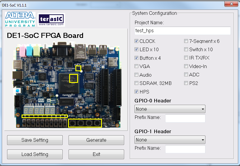
This utility generates a top-level file written in Verilog with declarations of selected elements. We need CLOCK, HPS (SoC), buttons, LEDs. By clicking Generate we get the Quartus project. The main advantage of creating a project in this way is that we do not have to assign FPGA pins to Pin Planner, because the utility did this for us, thereby saving a lot of time.
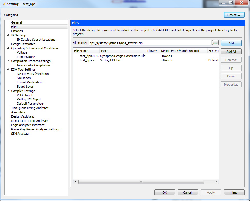
Add the generated file to the project.
The next step is to create a system in QSYS. Just in case, I will briefly explain the essence of what is happening. Cyclone V SoC is not just FPGA, inside its structure is a dual-core Cortex-A9 processor with various modules, such as USB ports, Ethernet, SPI, SD / MMC, etc. In a simple way, you can imagine this as a microcontroller inside the FPGA. Creating a system in QSYS we connect the HPS (hard processor system) system with the elements synthesized in FPGA using ready-made kernels (IP cores). QSYS allows you to connect different cores through the Avalon-MM or AMBA AXI buses without unnecessary worries, we do not need to write code manually, QSYS generates it for us. We go into QSYS and select our HPS system in the IP cores tab. In the system settings, we need only Lightweight H2F Bridge in the FPGA interfaces tab.

In the Peripheral Pins tab, select SD / MMC (we will download the program from the card) and UART. We will tell you more about this later.

In the HPS clocks tab, we leave everything by default. In the SDRAM tab, you need to fill in all fields with skew values and so on. As far as I understand, they depend on the trace of lines from the microcircuit to SDRAM. I could not find any document that contains this data for DE1-SoC, so I took it from a finished project for my board (it was SOC-Computer in the examples of the Altera University Program). I saved these settings as a perset, so I don’t have to fill them anymore, you can see it in the right column. Next in IP cores we find PIO, these will be our LEDs and buttons.
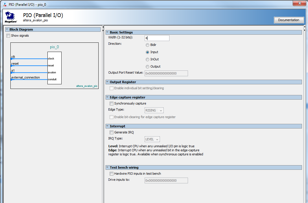
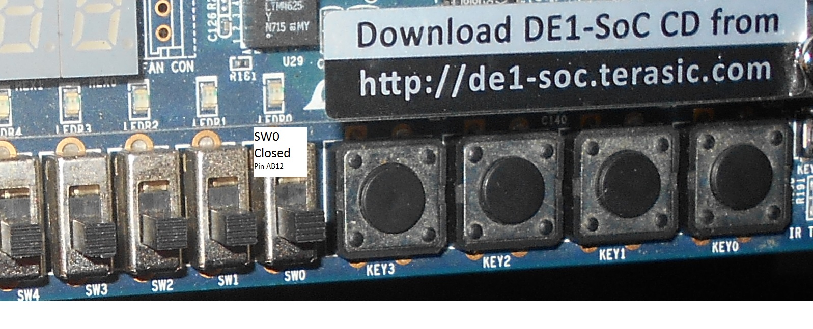
For the button settings, select Input and a width of 4 bits since 4 buttons in total
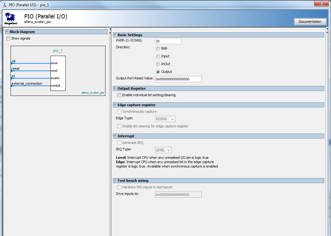
For LEDs, respectively, Output and width 10. We
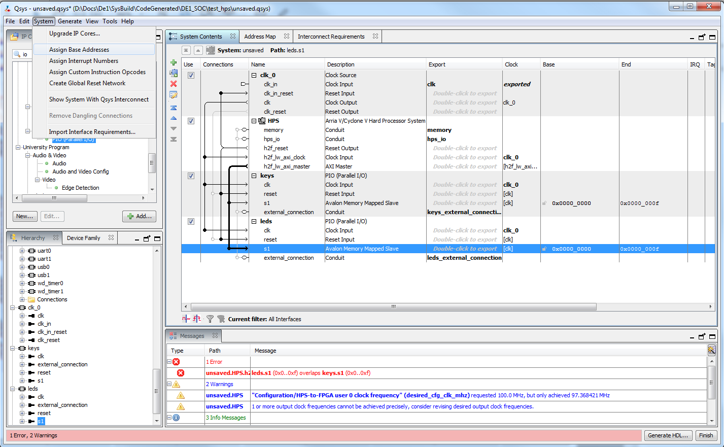
connect the resulting system as shown in the figure. We can change the PIO names so that it is more understandable and beautiful. The LWH2F bridge is the link between the HPS and the FPGA (also appointed as the HPS master), since PIOs are elements that run in the FPGA fabric. Double-click on the inscription “Double click for export” opposite the external connection, in order to output the PIO LEDs and buttons from the system. Later, you will see these findings in the top-level code of the generated system file. Since access to the PIO, and to all other cores, in HPS is done at addresses, you must assign them. This can be done automatically by clicking Assign base addresses.
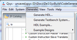
After that, you can generate the system code.
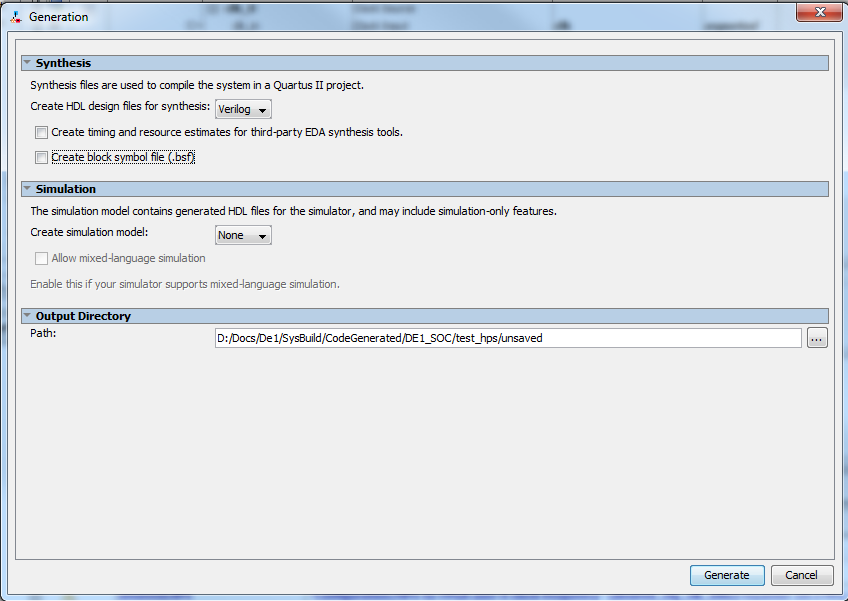
We indicate the path and the desired code language. I prefer Verilog. After that, QSYS can be closed. The following message appears in the Quartus window:

Let's do what we are asked.
In the Files window, we see our hps_system.qip. We open it and see the top-level file of the system.
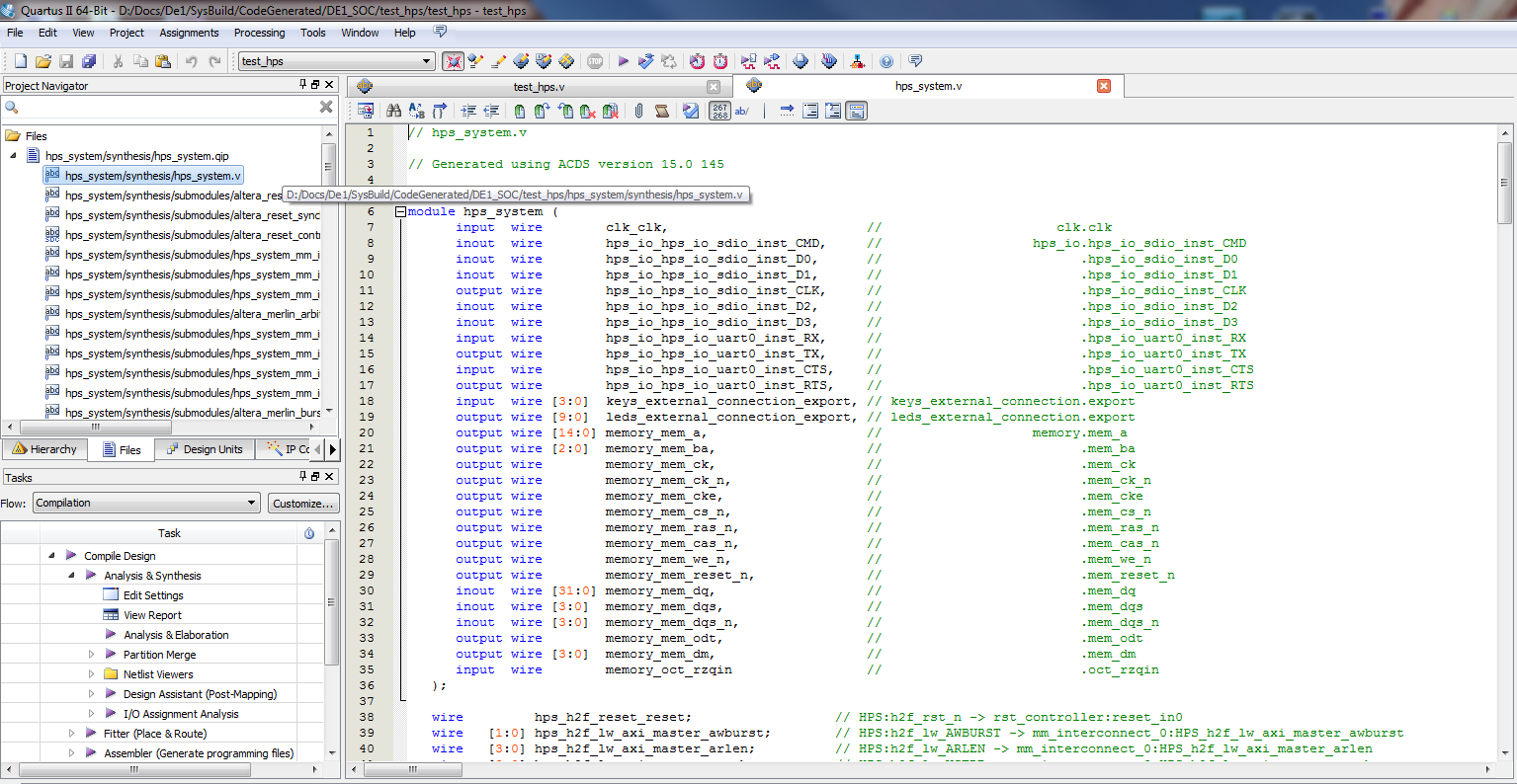
Everything that we have chosen in the QSYS system is now in this file. Now you just need to insert this module into the original file. This will be the top-level file of our FPGA firmware.
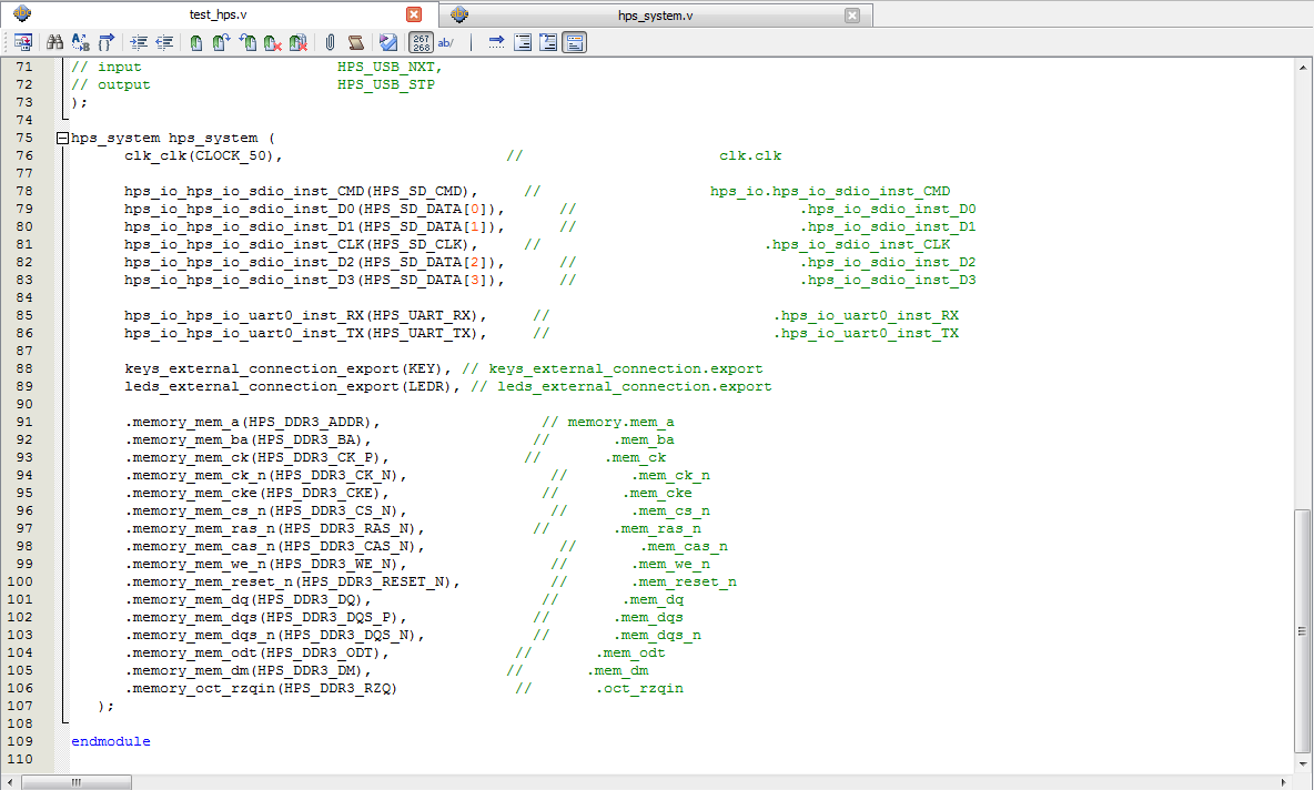
In it, we assign the initial I / O pins of this file to the HPS system pins. I remind you that nothing needs to be assigned to Pin Planner, everything has already been done when creating the project with a utility. But you need to assign HPS pins, this is done as follows:
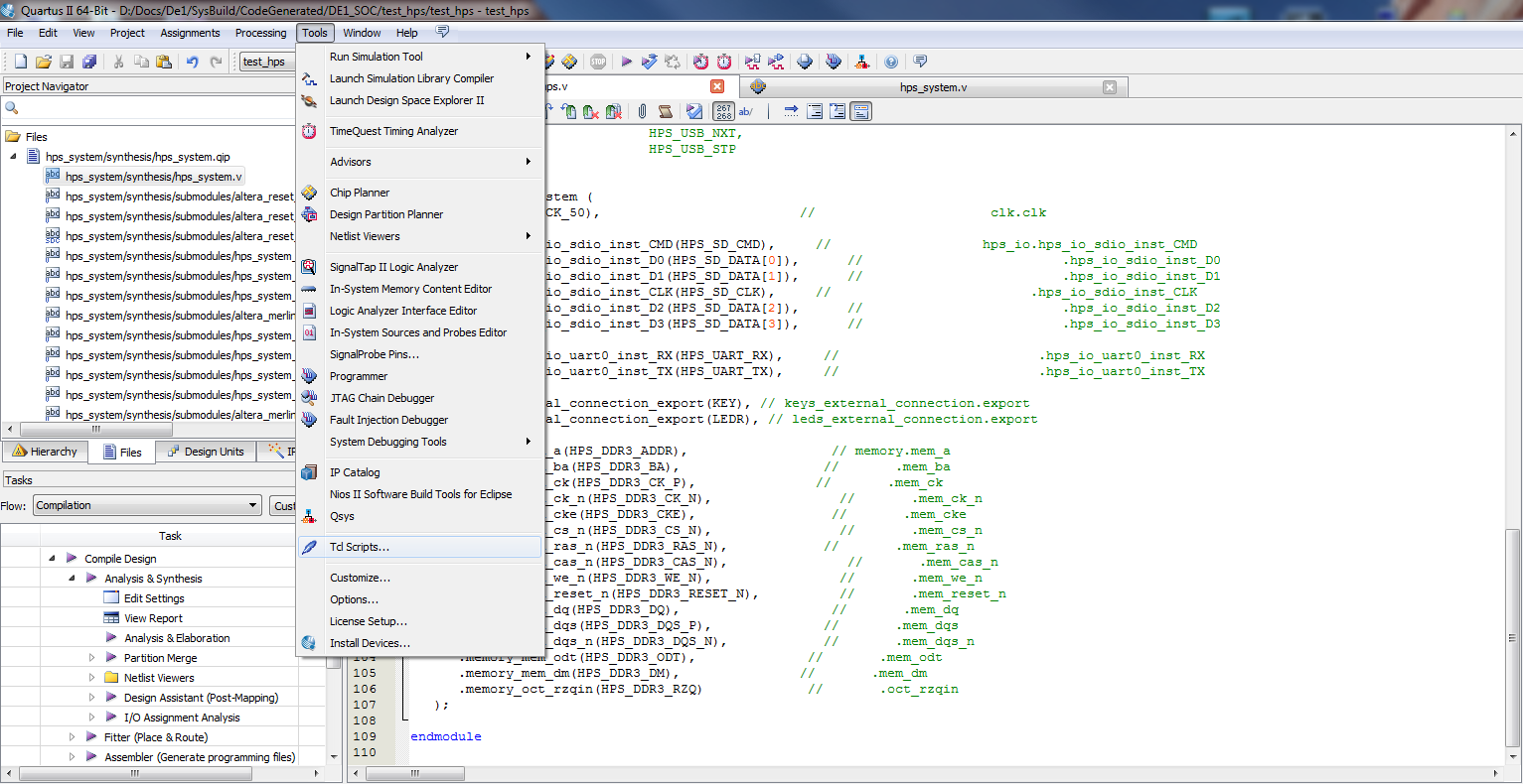
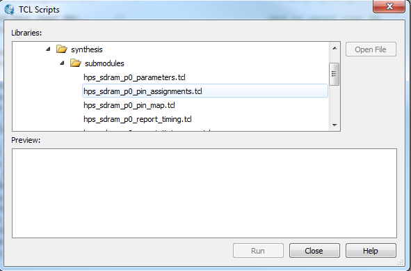
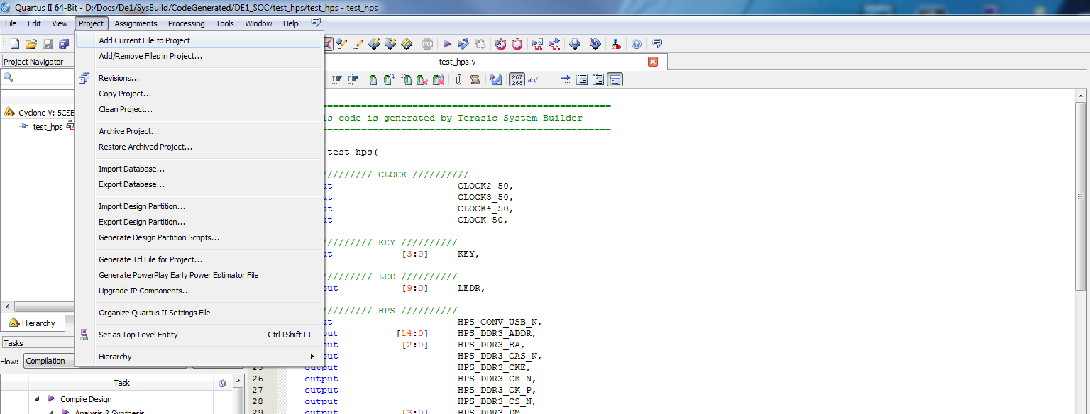
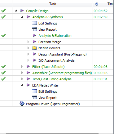
Once this is done, you can compile the firmware. It is important to note that if any errors were made (for example, I forgot to put an end to the hps_system declaration near clk_clk and hps_io_hps_io_ ... it can be seen from the figure), tcl scripts must be run again. Even if everything is written correctly and you run tcl scripts, but after starting compilation you get an error, it’s worth trying to run the scripts again without changing anything in the code. It helped me, I don’t know how to explain this feature.
And so, with the firmware finished! Now let's start creating Preloader.
Create Preloader
The HPS boot process has several stages, let's try to understand them. It is worth noting that Cortex-A9 is a processor for applications, the letter “A” in the name means Application, and is primarily designed to work using an OS, such as Linux. Therefore, strictly speaking, the idea of launching Bare-Metal programs may seem strange, but in some cases it is necessary. In addition, of course, there is such an opportunity, but the developer needs to understand the loading process at least at a basic level.
Immediately after switching on, the code located directly on the Cortex-A9 Flash memory called BootRom is executed. You cannot change it or even see its contents. It serves for primary initialization and in the next step transfers the boot process to SSBL (Second Stage Boot Loader, shortly called Preloader). What you need to know to understand the process is that BootRom code, first of all, selects the Preloader download source, focus on the external physical BSEL pins. In the DE1-SoC, the initial configuration of the pins for loading from the SD card was initially selected, and changing it to, for example, QSPI or NAND flash, without soldering an additional switch and a pair of resistors, is impossible. Therefore, in QSYS, we selected the pins of the SD card in the Peripheral Pins tab. There is also a boot option not from external sources, but from the memory created in FPGA,
And so, after the BootRom code is executed, the Preloader, which is necessary for setting Clock, SDRAM and other things, starts loading. After the program starts to run.
To create Preloader, you need SoC EDS, I'm sure you have already downloaded it from the Intel FPGA website.
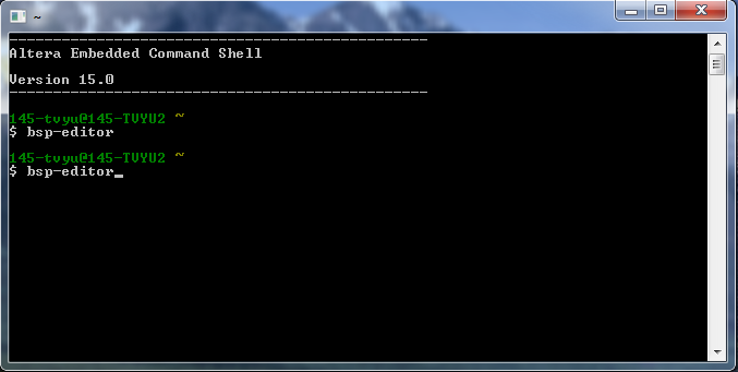
The program works from the command line. First, create a BSP by writing the appropriate “bsp-editor” command.

In this window, click New HPS BSP.

You must specify the path to {Project directory} / hps_isw_handoff / and click OK, you do not need to change other parameters.
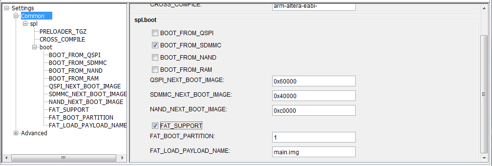
We select the spl.boot settings in which we indicate the source where Preloader will be loaded from. In our case, this is an SD card, so choose BOOT_FROM_SDMMC. We will use the download option for Preloader and our program in which the flash drive has at least 2 partitions - the partition is not formatted with id = A2, for Preloader, and the partition with the FAT32 system, for the program. There is another option without dividing the flash drive into partitions, the so-called RAW format, but our option is simpler in my opinion. You can format a USB flash drive in this way with any program (I used Mini partition tools 9.2). Or you can use the already-assembled image in the folder ... \ embedded \ embeddedsw \ socfpga \ prebuilt_images \ sd_card_linux_boot_image.tar.gz and write it to a USB flash drive through Win32DiskImager.
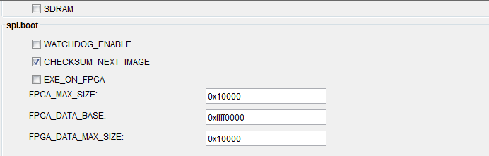
Choose FAT_SUPPORT, FAT_BOOT_PARTITION 1, FAT_LOAD_PAYLOAD_NAME .img. We will not use WATCHDOG_ENABLE and EXE_ON_FPGA (we are not going to download Preloader from FPGA).
Here is a very delicate moment at which I fell for a whole month looking for a problem when I was just getting acquainted with SoC. Serial Support means that already Preloader will use the UART module to display diagnostic messages right at boot time. Semihosting means that during the output of these diagnostic messages, they will be automatically displayed in the debugger window during debugging. Using this function in the program itself is very convenient; it allows you to display everything written in the printf function in the debugger window without additional writing code. If in the QSYS settings in HPS you do not specify the use of UART, but check the Serial Support checkbox in BSP - this Preloader will not work. If you remove Serial Support, while leaving Semihosting, nothing will work either, at least I had it. So you can experiment or just check the box if you want everything to work. Click Generate, then Exit.

Now change the working folder of the SoC EDS with the cd command "<specify the full path to the generated BSP files (by default it is ... software / spl-bsp)>" To build Preloader, execute the make command. We are waiting. At the end of the process in the package we get the desired file preloader-mkpimage.bin.
This is a compiled file in which there are 4 identical Preloader images. With the mkpimage command executed in SoC EDS, you can parse this file into components (separate images), and then assemble it from other configurations (with different Preloader images). Other configurations can be completely different (different systems in QSYS), that is, we get separate preloader-mkpimage.bin files with 4 identical images (64kb each), disassembled them into components and now you can build a new preloader-mkpimage.bin with different images (for example, with different download sources). This is done for reliability. Suppose it happened that some kind of force did not allow to boot from the first attempt, from the first image. Then the second image starts loading, and it, for example, is slightly different for us, for an emergency. If this one failed to load, then move on to the third and so on. But this is no longer the subject of our task, rather a lyrical digression from the topic, so continue!
Insert the USB flash drive with the already prepared section A2 and write to it our preloader-mkpimage.bin with the command "alt-boot-disk-util -p -a write –d". SoC EDS should point to the path to the folder where the Preloader file is located. Everything is almost ready to write a program! Just create header files with QSYS element defines for convenience. Change the path of the SoC EDS, pointing to the firmware file, and run the command sopc-create-header-files .sopcinfo. At the output, we get several files, looking at the contents of which it becomes clear why they are.
Program
For writing and debugging the program, the manufacturer recommends using the DS-5 Eclipse environment. It is recommended to start Eclipse through the EDS SoC with the “eclipse &” command (the “&” sign at the end of the command is placed so that the EDS SoC window is active after opening Eclipse).
For those who are already familiar with ARM and have ever written programs for such an architecture, the difficulties end. For those unfamiliar with ARM, difficulties continue.
Create an empty “C” project. There will be a compiler selection window, here everyone is free to choose and understand what suits him best. As a newcomer to ARM, I liked Arm Compiler 5 more, mainly because of the relatively simple syntax of scatter files used to place the written program in different parts of the program (the mere appearance of the GCC linker script syntax scares me). In the project settings, everything looks trivial. I will only point out this command.
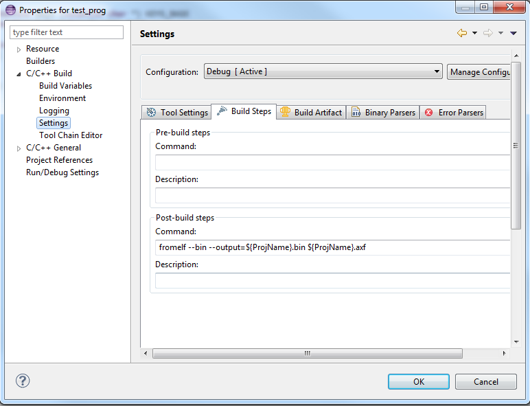
Do the same. This converts the axf format to bin format. We will need this later to record the program on a USB flash drive. We will finally write it.
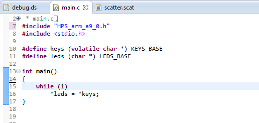
Here even stdio.h is not required. This program simply assigns the contents in memory to the address KEYS_BASE for the address LEDS_BASE. By pressing a button on the board, the LED will turn off that hour.
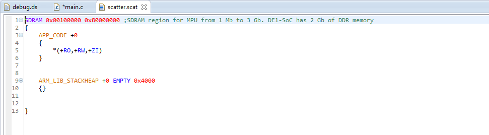
The contents of the scatter file.
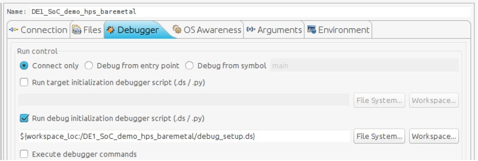
For debugging, you need to write a script in debugger. As you recall, the download process is not easy. The script stops the execution of Preloader at the stage of downloading the application from the source and transfers this task to the computer.
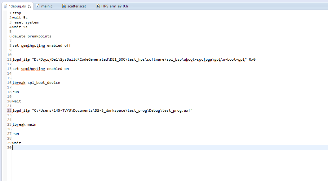
Do not forget to flash the board before downloading the program and debugging!
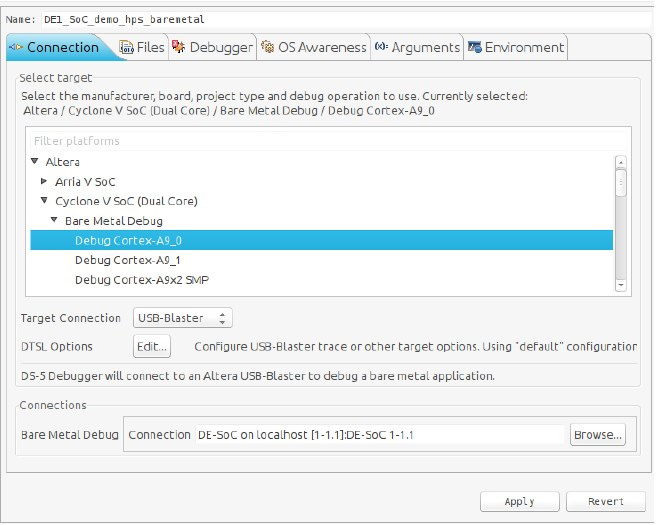
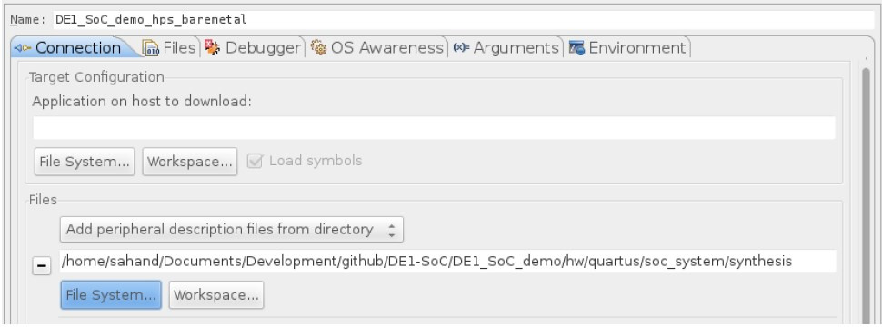
In the debug window, you need to create a new task, this is done in Debug control. I forgot to take screenshots at this stage, so I borrowed them. Apply the settings similar to those in the pictures below.
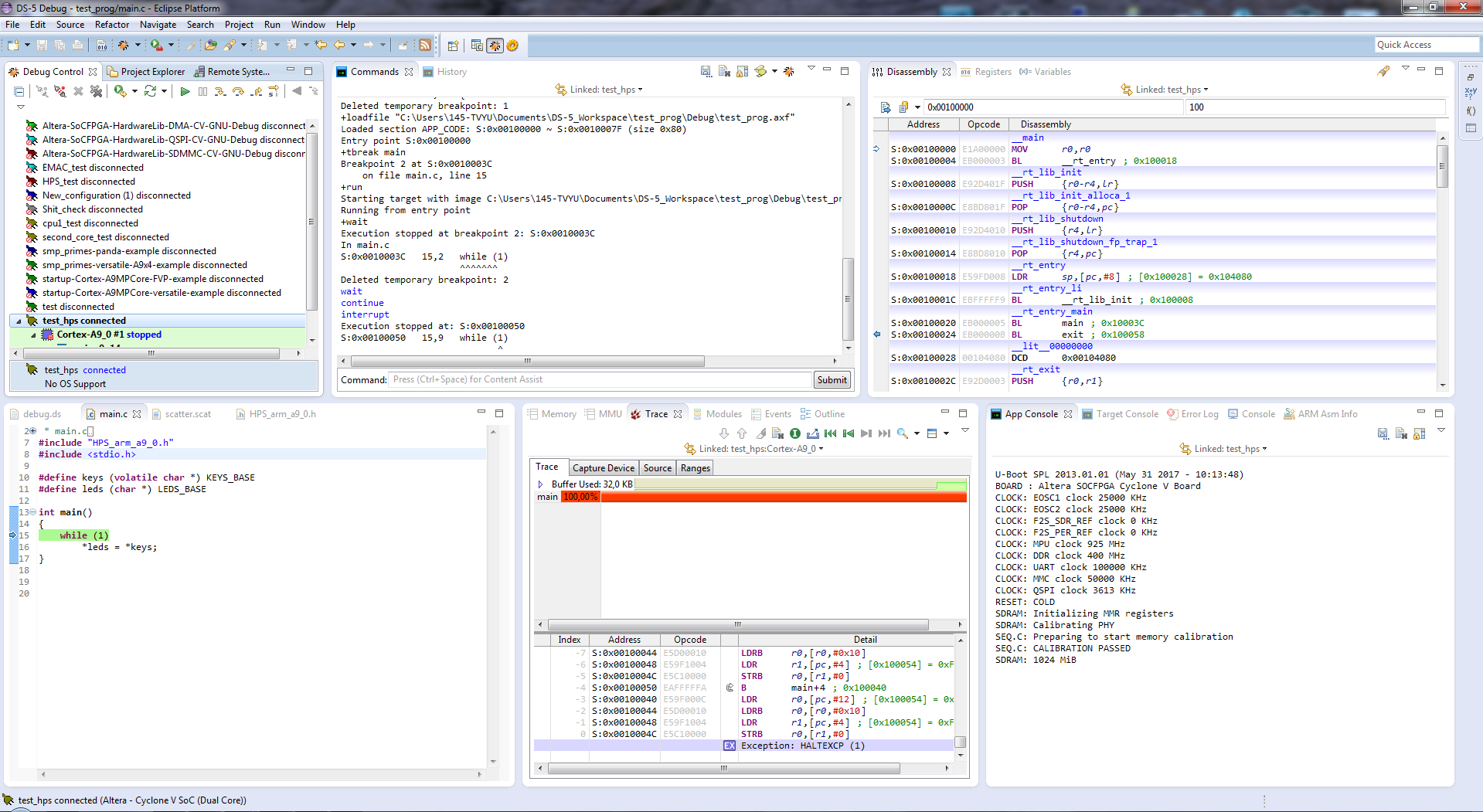
Now, after compilation, you can debug the program, look at the contents of the registers and do a lot of interesting things.
After you have made sure that the program works correctly, you can create an image of the program for self-loading. To do this, from the Debug folder with the DS-5 project, we take the file
The entry point can also be set in the project itself, if interrupt vectors are used, we do not use them, so we do not set it. I am guided by what addresses I set in the scatter file, and I write the same in this command. Before execution, do not forget to specify the path to the bin file in the SoC EDS with the cd command "<file folder>". The name of the img file must match what you specified in the BSP editor in FAT_LOAD_PAYLOAD_NAME.
Now just copy the file to the USB flash drive in the fat section, like a regular file.
Conclusion
In this article, many points could be considered in more detail, since the described process has many stages, and each has alternative options for implementation and its own characteristics. But I think that for all other questions the list of references will perfectly answer for me. Read the following article Launch AMP Applications on Cyclone V SoC