UDB. What is it?
- Transfer
In the comments to my article about controlling RGB LEDs using the UDB block of PSoC microcontrollers from Cypress, it was suggested that it would be nice to briefly tell at the beginning of the article what UDB is. As I noted in the article, briefly not to write about UDB, but you can simply translate corporate documentation to it, in order to acquaint the domestic reader with such a powerful tool for implementing microprogram functions.
But first, let's look at what PSoC is. PSoC is a Cypress chipset family for implementing on-chip systems. Different families have a different processor core (for the PSoC 3 this is the MCS-51, for the PSoC 4 - the Cortex M0, for the PSoC 5LP - the Cortex M3, and for the PSoC 6 - two at once: Cortex M0 + and Cortex M4) and a set of programmable logic. And this logic is not purely digital, there are analog things there too. In addition to a set of different ADCs, there are also analog switches. You can even programmatically link the legs through analog circuits, however, the resistance of the circuit will be measured by kiloiom. There are inside PSoC and operational amplifiers, which can be switched by software, which means - to build different analog blocks on them.
By the way, PSoC'i can be powered by any voltage from 2.7 to 5.5 volts. That is, you do not need to think about any stabilizers, either with battery power or with USB power.
But about analog things, I wrote purely to be nice. Now we will focus on digital things. Most modern controllers have powerful peripheral units that provide a huge variety of functions. But in practice, in each specific software development, these blocks are not used completely, but only partially. And in PSoC, instead of a heap of good, a program logic is implemented that is similar to the logic of classic FPGAs. Accordingly, it is possible to implement exactly those blocks that are needed by including them in exactly those modes that are required. And not to spend resources on unused modes, having given them for realization of some own things.
And here often some misunderstanding arises. Many developers are accustomed to the fact that Programmable Logic Integrated Circuits (FPGAs) are of two kinds: CPLD and FPGA. Therefore, many who have heard about PSoC, believe that there lies a certain CPLD-scale, which can be programmed in Veriolg. In fact, both yes and no. A certain number of PLDs (without “C”, just PLD) are really there, and you can really program them on Verilog. But really, these PLDs are part of the UDB blocks. And it is UDB that is the main element of programmable logic implemented in PSoC. This unit is extremely distinctive and provides simply a tremendous opportunity for the developer. Consider the figure from the company documentation, explaining the essence of the use of UDB blocks.
Since I studied everything using the example of the PSoC 5LP family, I will transfer the documentation to him. But before you start, I will say a few words about the price of these controllers. If you go to Ali Express and look at the design boards for them, a sad feeling arises. Frankly speaking, compared with the STM32-DISCOVERY, they are still nothing, but on the background of the STM32F103C8T6 prototypes are expensive. First of all, this is due to the fact that there is always not one, but two such controllers on branded layouts. JTAG functions are implemented on the PSoC 5LP, even if the target controller and PSoC 4 (the latter usually does not have a USB port).
But even by dividing the price by two, we still find that it is higher than that of the similar in processor core STM32F103. However, if we add to the very same STM32 outside even the most unpretentious CPLD, then the total price will already be released in favor of PSoC. And we also add the lost legs to the connection of these two buildings (for PSoC, all the connections are inside). And the price of square centimeters of the board. So it turns out that if you only need to work with the processor core, there really is no need for PSoC. If you need to bring some functionality to the firmware or hardware level - then you need PSoC. On it, the system will be cheaper and easier.
In fact, I have a manic idea to try to make hardware support for the core of our RTOS MAX. To do this, I studied the methodology for developing Bare Metal applications for Altera V SoC (alas, it turned out that the architecture is such that the OS can be slowed down, but it cannot be accelerated - single requests to the hardware there come with a frantic latency). For this, I began to master PSoC. I still haven't gotten to overclocking the kernel (there are only general thoughts), but I really liked the idea of programming UDB. Of course, I am now interested in bringing this idea to the maximum number of domestic programmers. Therefore, we proceed to the translation of the relevant part of the Cypress UDB dedicated documentation. The numbering of chapters and drawings is preserved in accordance with the original document.
UDB. What is it? Part 1
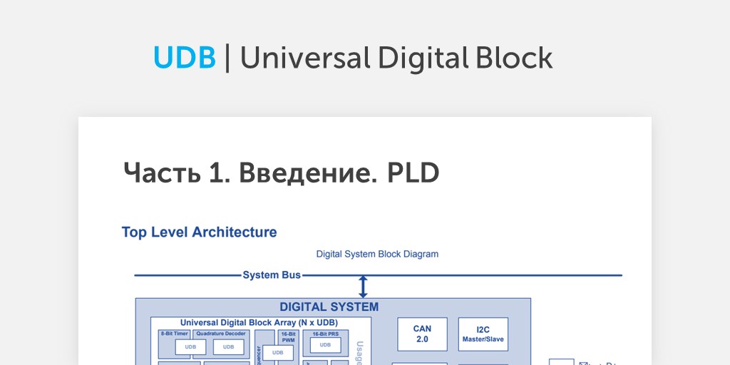
21. Universal digital blocks
In this chapter, we look at how universal digital blocks (Universal Digital Blocks (UDB)) allow us to develop programmable digital peripheral functions. The UDB architecture provides a balance between the granularity of the configuration and the efficient implementation. UDBs consist of a combination of uncommuted logic, similar to a programmable logic matrix (PLM, eng. PLD), structured logic (operational automata, hereafter referred to as Datapath) and a flexible trace scheme.
21.1 Features
- To ensure optimal flexibility, each UDB contains the following components:
• 8-bit ALU-based Datapath (Arithmetic and Logic Unit, ALU) with 8-word instruction, multiple registers and FIFO buffers;
• two PLDs, each of which has 12 inputs, eight conjunctive terms (English Product Terms, PT) and four outputs of macrocells;
• management and status registers;
• clocking and reset modules. - PSoC 5LP contains an array of up to 24 UDB in size.
- Flexible tracing between UDB array elements.
- UDB elements can be split or chained to create larger functions.
- Flexible implementation of a number of digital functions, including timers, counters, pulse-width modulators (including PWM with dead-zone generator), UART, I2C bus, SPI bus, and CRC checking / generation.
21.2 Block Diagram
Figure 21-1 shows a UDB in the form of a construct containing two basic logical blocks PLD, Datapath and control functions, status, clocking and reset.
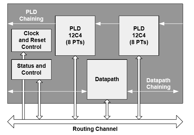
Figure 21-1. Block diagram of UDB.
21.3 How it works
The main components of UDB are:
- PLD (2). The inputs of these blocks are supplied with data from the trace resources. They implement combinational logic and data latching, which allows you to implement state machines, control the operations of the Datapath block, configure input conditions and control the outputs.
- Datapath. This block contains a dynamically programmable ALU, four registers, two FIFO buffers, comparators, and condition generation.
- Management and Status (Status and Control). These modules provide a mechanism for interfacing the central processor firmware (CPU) and synchronizing with UDB operations. Management registers affect internal elements, and status registers read the state of external elements.
- Clock and reset control. These modules provide the selection and activation of clocking, as well as the selection of a reset within the UDB.
- Chaining Signals. PLD and Datapath have signals that allow you to link adjacent blocks in a chain to create functions with a higher bit depth.
- Routing Channel. UDBs are connected to a trace channel through programmable switching matrices for communication between blocks within one UDB and for communication with other UDBs in the array.
- System Bus Interface (Sysytem Bus Interface). All registers and RAM in each UDB are projected onto the system address space, and access to them can be obtained both with the help of a central processor and through direct memory access (Direct Memory Access, DMA) in the form of 8-bit and 16-bit data.
21.3.1. Pld
There are two 12C4 PLDs in each UDB. The PLD blocks shown in Figure 21-1 can be used to implement state machines, process I / O data, and create table logic (the Lookup Table, LUT). In addition, PLD can be configured to perform arithmetic functions, set the sequence of Datapath and generate status. Common logic can be synthesized and projected onto PLD blocks. This section provides an overview of the PLD architecture.
PLD has 12 inputs that transmit information to 8 conjunctive terms in the AND array. In each conjunctive term, you can choose direct (true, T) or inverse (complement, C) input. The output of conjunctive terms goes to the input of the OR array. The letter 'C' in 12С4 shows that the OR terms are constant for all inputs, and each OR input can get program access to any conjunctive term. This structure provides maximum flexibility and ensures that all inputs and outputs can be moved.
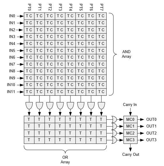
Figure 21-2. PLD 12C4 structure.
21.3.1.1 Macro PLD
The macrocell architecture is shown in Figure 21-3. The output controls the trace array and can be latched or combinational. D-flip-flop with direct or inverse input or T-flip-flop with high or low input level is used for latching. The output trigger can be set or reset upon initialization or asynchronously during normal operation, by an external signal from the trace channel.
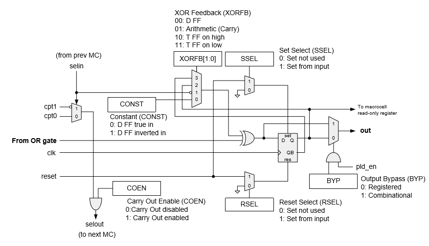
Figure 21-3. Macrocell architecture.
PLD "read-only" macrocell register
In addition to controlling the trace array, the outputs of both PLD macrocells are projected onto the address space as an 8-bit read-only register, which can be accessed using a CPU or DMA.
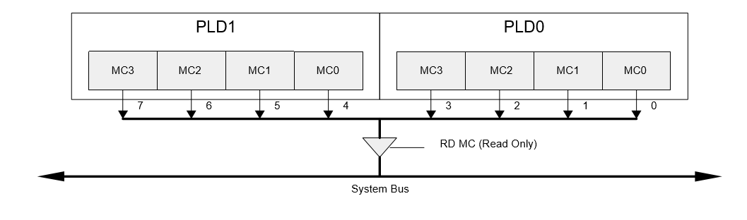
Figure 21-4. PLD read-only macrocell register.
21.3.1.2 Carrying chain PLD
PLD are tied together in UDB addressing. As shown in Figure 21-5, the selin carry chain enters from the previous UDB in the chain, through each macrocell in both PLDs, then goes to the next UDB as the output of the selout chain. To support the efficient placement of arithmetic functions, special conjunctive terms (PT) are generated, which are used in macrocells together with a chain of hyphenation.
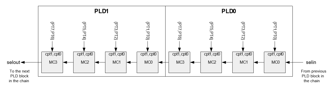
Figure 21-5. PLD carry chain and special conjunctive term inputs.
21.3.1.3 PLD Configuration
Each PLD is presented to the CPU or DMA as 16-bit access RAM. The AND array has 12 × 8 × 2 bits or 24 bytes for programming, and the OR array has 4 × 8 bits or 4 bytes for programming. In addition, each macrocell has one configuration byte, for a total of 32 configuration bytes per PLD. Since each UDB has 2 PLDs, the entire configuration of each UDB is 64 bytes.
Next time we will look at Operational Automata (Datapaths).