Automated design of electronic equipment
 The popular form covers the issues of computer-aided design of electronic equipment (REA) on printed circuit board designs, the main stages of the formation and evolution of computer-aided design systems (CAD) REA, the content of automation tasks, the organization of the end-to-end cycle of design work using automation tools.
 The purpose of the publication is to familiarize engineering and technical workers with one of the rapidly developing areas in the modern information technology industry.
Foreword
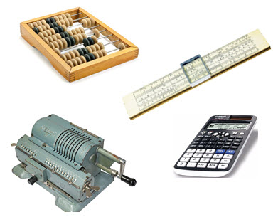
Automation of design and accounting activities in engineering practice has a long and fairly rich history. Turning to the relatively recent past, it suffices to recall the scores, mechanical arithmometers and slide rules. Somewhat later, electronic calculators were included in the calculation practice, which until now have been widely used. All these devices are aimed at facilitating the implementation of a variety of calculations, a significant proportion of which is in the design activities of engineers.
 An important step towards the automation of accounting activity was the emergence of electronic computers (computers), the capabilities of which allowed not only to perform calculations, but also to control the flows of necessary calculations and data by compiling programs in specialized programming languages: Autocode (or Assembler), Algol, Fortran and others. Programming has fundamentally changed the applicability of the mathematical methods of algebra, geometry, numerical methods, probability theory, operations research, discrete mathematics, linear programming, and many others that have been developed over the centuries. Improving the performance of computers (speed and size of RAM) with the simultaneous expansion of the range of peripheral devices: input-output textual and graphic data, drives for long-term storage of information, as well as the intensive development of operating systems, compilers of programming languages have had a significant impact on the changing role of computers in engineering practice. The solution of individual design tasks was gradually replaced by the completion of the completed stages of the project cycle, which gave rise to the concept of computer-aided design in accordance with the following definition.
Computer-aided design system - an automated system that implements an information technology for performing design functions, is an organizational and technical system designed to automate the design process, consisting of personnel and a set of technical, software and other means of automating its activities. Also to denote such systems is widely used abbreviation of CAD .
The main purpose of CAD is to improve the efficiency of engineering: reducing the labor intensity and design time, ensuring high quality design solutions and documentation, minimizing full-scale simulation and testing of prototypes, reducing the cost of pre-production.
In modern engineering practice, the most widely used are the following types of CAD:
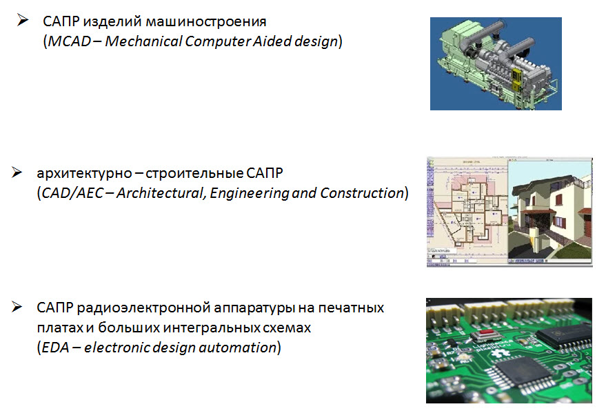
The content of this publication is limited only to issues related to the subject area of CAD electronic equipment on printed circuit boards.
In 1948-1950, William Shockley created the theory of the pn junction and a junction transistor, and the first such transistor was manufactured on April 12, 1950. In 1954, Texas Instruments released the first silicon transistor. A planar process based on silicon has become the main technology for the production of transistors and integrated circuits.
 For collaboration in the development of the world's first transistor in 1948, John Bardeen, William Shockley and Walter Brattein shared the Nobel Prize in 1956. The formation and development of industrial technology for semiconductor devices has determined the long-term and stable growth trend of the degree of integration of electronic components, the transition to semiconductor components has significantly expanded the field of application of electronic devices with a dramatic increase in their degree of integration and, as a result, functional complexity.
The expansion of the range of applicability of electronic devices has also contributed to the progress in the production technology of printed circuit boards, which have high reliability of electrical connections and mechanical strength, which is a priority requirement for mobile and stationary electronic products.
The “birthday” of printed circuit boards is considered to be 1902, when the inventor, German engineer Albert Parker Hansen filed an application with the patent office of his native country.
Hansen's printed circuit board was a stamping or cutting image on a bronze (or copper) foil. The resulting conductive layer was glued to the dielectric - paper, impregnated with paraffin. Even then, taking care of the greater density of conductor placement, Hansen stuck the foil on both sides, creating a two-sided printed circuit board. The inventor also used through-going connecting holes. In the works of Hansen there are descriptions of the creation of conductors using electroplating or conductive ink, which is a powdered metal mixed with an adhesive carrier.
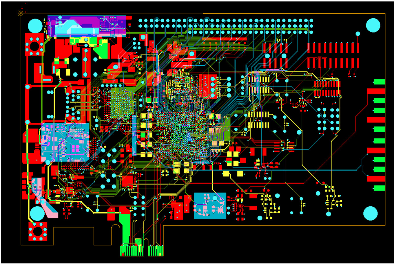
Printed circuit board (PCB)- plate of dielectric, on the surface or in the volume of which the electrically conductive circuits of the electronic circuit are formed. The printed circuit board is designed for the electrical and mechanical connection of various electronic components. The electronic components on the printed circuit board are connected by their leads to the elements of the conductive pattern, usually by soldering.
These trends in the development of circuit design and design of electronic equipment required radical changes in the approaches to the organization of processes for creating electronic products of high functional and design complexity, which stimulated the emergence of industrial computer-aided design systems for radioelectronic equipment.
At the first stages of the development of CAD REA, the main customers were enterprises — creators of complex computing complexes, whose general designers began to organize specialized CAD divisions in the structure of their design bureaus.
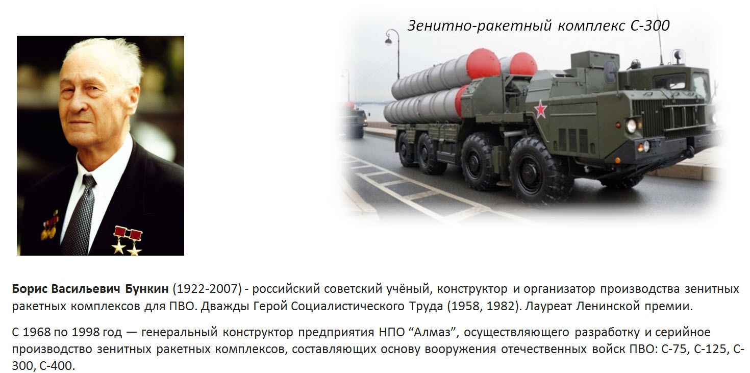
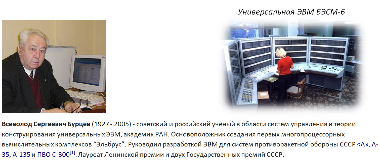
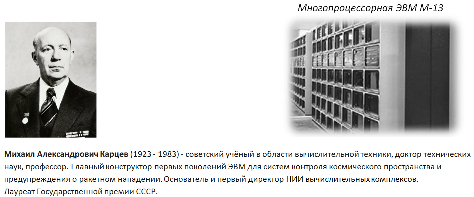
 Creating CAD REA required the use of effective mathematical methods and algorithms for solving key problems of structural and parametric synthesis of the designed devices. Researchers from leading universities: Moscow State University, Leningrad State University, Moscow Institute of Physics and Technology, Moscow Engineering Physics Institute, Moscow Engineering Institute, Moscow Technical University, Moscow Institute of Electrical Engineering, Moscow Aviation Institute, LETI and many others, as well as to polytechnic institutes of cities: Kaunas, Kiev, Lvov, Minsk. In order to integrate resources and coordinate the development of CAD REA in the USSR Ministry of Radio Industry, branch programs RAPIR and PRAM were carried out, aimed at creating information-compatible software packages for computer-aided design.
 The following scientists made significant contributions to the theory and practice of CAD, REA in particular:
Abrightis Lyudvikas Blazhevich
Bazilevich Roman Petrovich
Vermishev Hristoforovich Yuri
Zaitsev Zhanna Nikolaevna
Markarov Karpovich Yuriy
Matyuhin Nicholas Ya
Norenkov Igor Petrovich
Petrenko Anatoly
Ryabov Gennady G.
Ryabov Leonid Pavlovich
Seljutin Viktor Abramovich
Tetelbaum Alexander Y.
Shiro Gennady E.
Stein Marc Eliozarovich
and many others.
Structure and main stages of designing electronic equipment
Modern electronic equipment is implemented at the levels of the design hierarchy shown in the figure below. For all levels of the hierarchy, appropriate computer-aided design tools are used, such as CAD LSI / VLSI, printed circuit boards, blocks and cabinets.
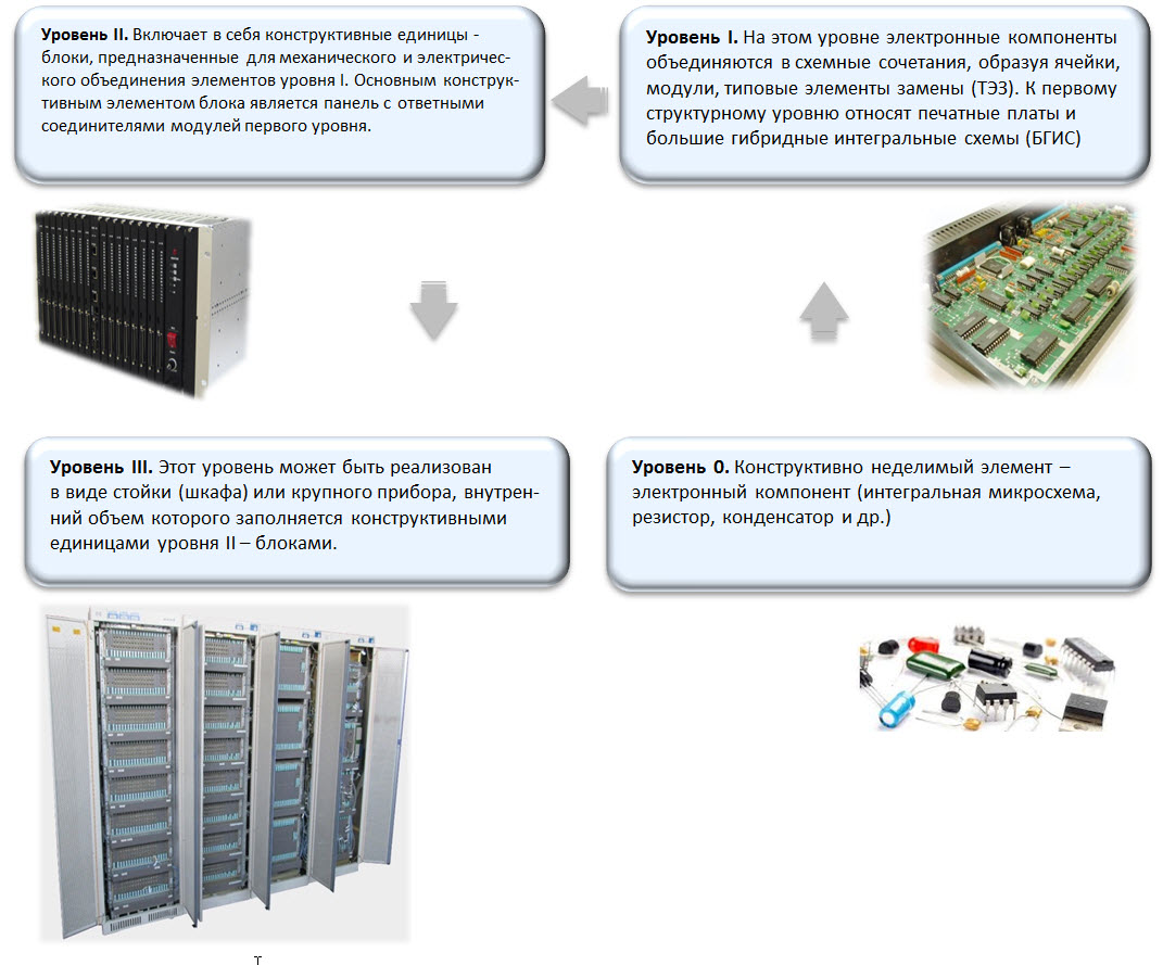
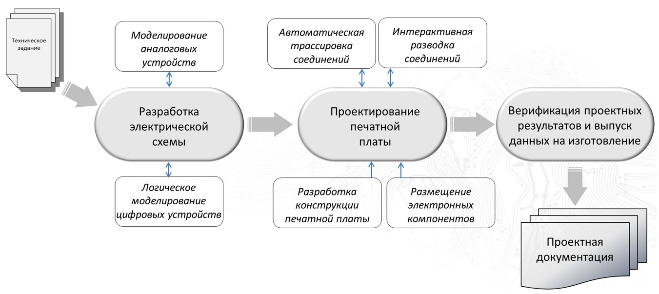
Next, we confine ourselves to questions of computer-aided design of standard replacement elements (Level I). The full cycle of designing electronic devices of level I includes the following main steps:
- The development of the electrical principle (E3) electronic device.
- Digital-analog simulation of the device circuit.
- Placement (arrangement) of electronic components and external connectors on the printed circuit board. Optimization of the component placement plan in order to minimize the length of the proposed electrical connections, ensure uniform thermal dispersion, create an acceptable electromagnetic environment for transmitting signals without distortion.
- Laying (tracing) of electrical connections between the equipotential terminals of the placed components in accordance with the specified design rules governing the width of the connections, the minimum allowable gaps with other elements of printed wiring, to ensure performance requirements and noise immunity.
- Control of the compliance of the printed circuit structure with the initial electrical circuit and technological limitations of production.
- Release of design and production documentation.
- Monitoring the integrity of project data, tracking changes, the exchange of project information with other automated systems.
Development of electrical schematic diagram (E3)
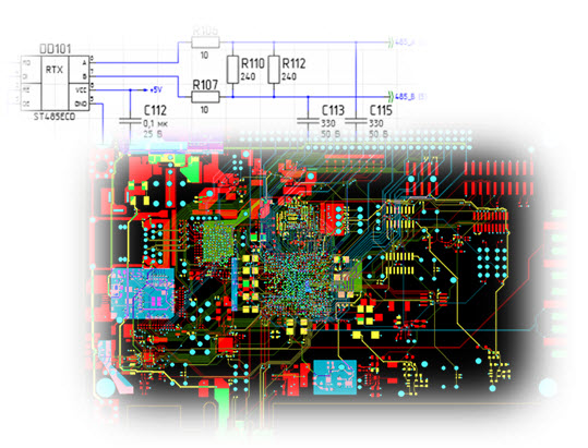
Electrical scheme - a graphic image used for transmission using conventional graphic and alphanumeric designations of the structure of an electronic device. Includes conditional graphic symbols (UGO) of electronic components and connections between their outputs.

A schematic diagram can be presented on one or more drawing sheets, and the diagram does not regulate the mutual (physical) arrangement of electronic components. All components on the scheme and connections are assigned unique identifiers (the component number according to the scheme, the name of the circuit, etc.). To improve the readability of the scheme, compact graphic objects are used - busbars and connectors.
The development of electrical circuits is carried out using pre-prepared and certified in accordance with the requirements of GOST libraries conditional graphic symbols of electronic components.
Logical simulation of digital devices
Logical modeling is one of the common ways to test the behavioral and functional properties of designed digital devices and is aimed at reducing the costs associated with the creation and testing of prototypes. The structure of a digital device for modeling is described in one of the most common languages for describing electronic equipment - VHDL and / or Verilog, and the values of signals in connections and the dynamics of their changes over time are displayed as graphical time diagrams.
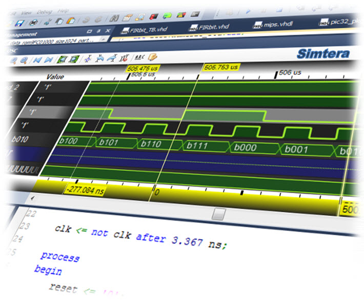
Modern software tools support the modes of logical modeling of asynchronous and synchronous digital devices in a multi-valued alphabet of possible signal values. Simulation and analysis of the joint operation of the hardware of a digital device and software (firmware) as part of this device is allowed, which ensures the integrity and completeness of the simulation results.
Simulation of analog devices
Simulation of analog devices allows for the analysis of operating modes and the estimation of circuit parameters without the manufacture of its prototypes.
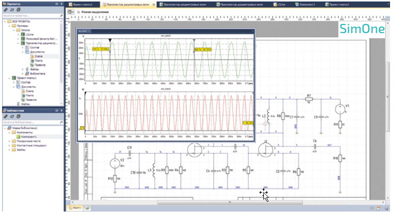
Currently, the following types of modeling analog devices are widespread:
- Analysis circuit for direct and alternating current
- Transient and transfer function analysis
- Noise and stability analysis
- Temperature analysis with changes in operating temperature
- Parametric analysis when changing the parameters of models of electronic components (transistors, diodes, capacitors, resistors, functional sources, etc.)
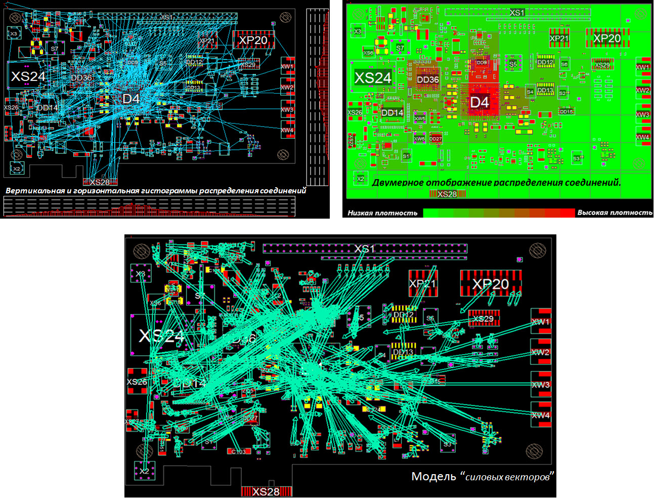
Placement of electronic components
Placement (placement) of electronic components and connectors on a printed circuit board is a complex task, which requires compromising on the following main criteria:
- Arrangement of components in compliance with the established rules for the minimum allowable distance between their housings and terminals.
- Minimization of the total length of the connections planned for implementation, taking into account the requirements for speed and noise immunity (differential pairs, functionally related groups, synchronization chains).
- Ensuring uniform distribution of the density of connections on the printed circuit board.
- Accounting for heat dissipation and electromagnetic radiation of electronic components.
In order to assess the quality of electronic components on a printed circuit board, assessments are used, in particular, related to the analysis of the density of the required connections or the model of “force vectors”, indicating for each component the direction to its best mounting spot on the board.
Electrical tracing
Connection tracing is a key step in the design of electronic equipment, and solves the problem of laying connections on layers of a printed circuit board between the equipotential terminals of components taking into account specified rules and restrictions, among which are the limitations on the width of conductors and the minimum allowable gaps between printed circuit elements. Indicators of the effectiveness of the applied methods of tracing are the completeness of the implementation of the electrical circuit, the minimum total length of the constructed connections, the number of layers used and interlayer transitions.
Currently, in practice, the following three methods (modes) of printed wiring are widely used:
- Manual tracing is performed by the designer by drawing a pattern of conductors on the drawing board.
- Automatic tracing is implemented by specialized programs that carry out layered wiring of conductors. The results obtained are available to designers for subsequent manual adjustments and modifications.
- Interactive tracing is a combination of manual and automatic tracing modes. In this case, the designer sets the conditions for tracing all or part of the required connections, and the software performs trace operations under the specified conditions.
Taking into account the fact that the results of automatic tracing are very critical for computer-aided design, the following are descriptions (in a fairly general form) of common algorithms for solving this problem.
Wave tracing algorithm for automatic tracing
For the first time, the description of the wave tracing algorithm of connections on printed circuit boards was published in the early 60s (Lee, CY, “An Algorithm for Path Connections and Its Applications”, IRE Transactions for Electronic Computers, vol. EC-10, number 2, pp. 364–365, 1961). The simplicity of this algorithm was the impetus for the implementation of a variety of appropriate software.
At each iteration, the algorithm searches for and forms a joint of a given width between two given points on a plane, taking into account the existing obstacles. To perform these functions, the so-called discrete working field (PDD) is used - a two-dimensional numerical matrix, the cells of which display the corresponding parts of the printed circuit board with dimensions equal to the width of the conductor, increased by the value of the allowable gap. This ensures that two conductors placed in adjacent cells will always have the required gap between their edges. PDD cells prohibited for laying connections are marked with special labels.
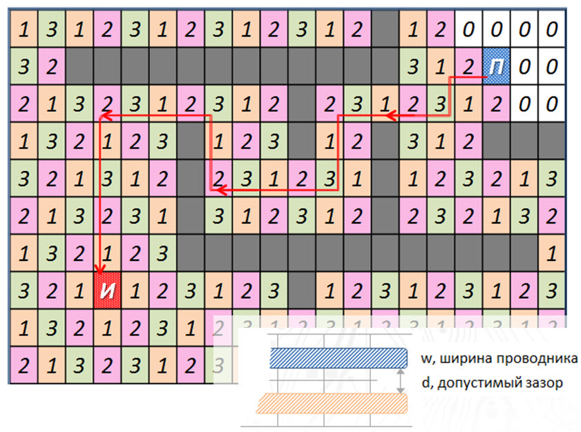
The connection search is performed by sequential assignment of 1-2-3 numeric tags to ... adjacent (not prohibited for the connection construction) PDD cells, starting with one of the connected ( “AND” ) and before the second ( “P” ) meet . In the case when the second connecting cell is reached, the formation of the found connection starts from it on the basis of the sequential selection of pairs of neighboring cells in the code sequence ... 3-2-1-3-2-1 ... The
constructed connection is displayed on the PDA with a new set of connections prohibited for laying cells and then the procedure described is repeated for a subsequent pair of points, etc.
Geometric tracing methods
Geometric (shape-based) tracing methods make up the next-generation wave generation of PCB tracing algorithms and large integrated circuits.
These methods operate on geometric models of objects of printed wiring (contacts, conductors, etc.), carrying out the search and laying of connections in the existing maze of free resources.
Algorithms of this class solve the problem of laying each connection also in two stages: the search for a possible connection and its installation.
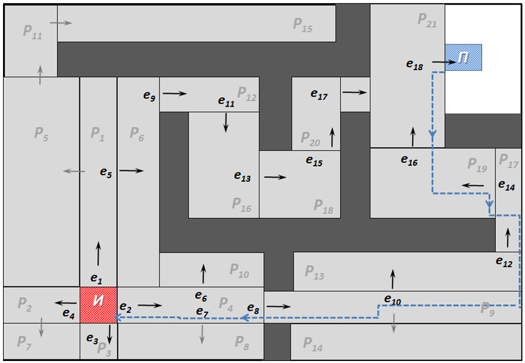
The connection search is performed by sequential distribution of rectangular samples ( “AND” - initial sample) over continuous sections of available trace resources - until a meeting of the “P” geometric object(or the exhaustion of all resources). Each formed sample is a source for the formation of three generated samples along its edges (e N ).
Found path is defined as a sequence of pairs of generating and generated samples
( П e 18 e 16 e 14 e 12 e 10 e 8 e 2 И )
Methods of topological tracing
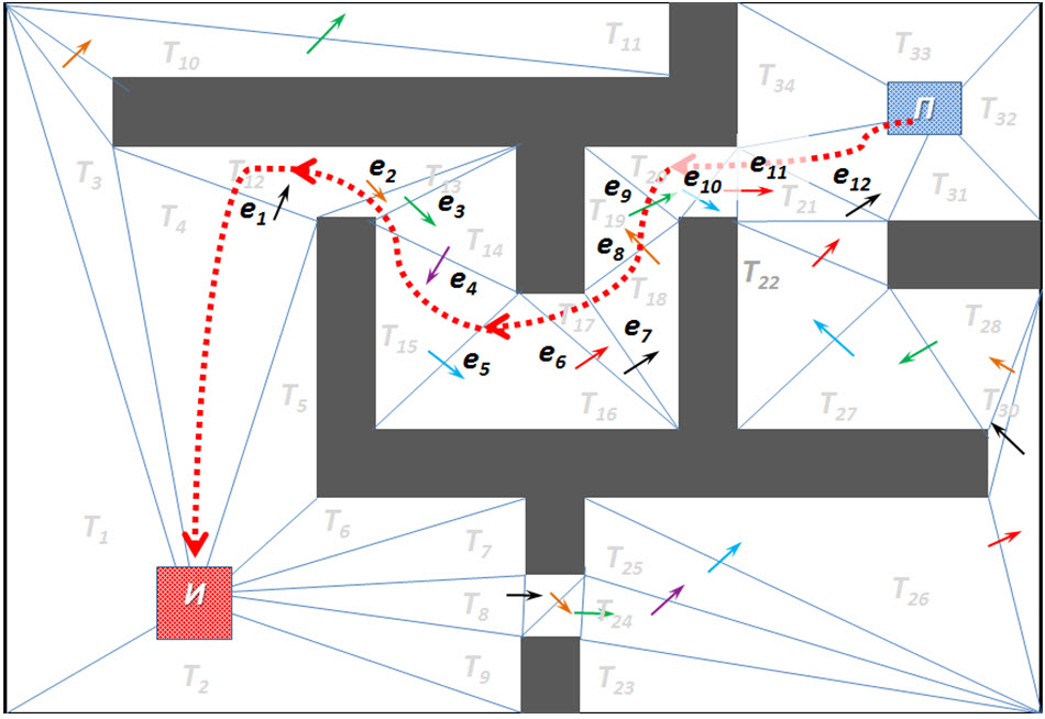
Topological tracing methods operate with a topological model of tracing resources, formed as a result of applying triangulation operations (or similar based on convex polygonal geometric figures) to a set of characteristic points of printed wiring elements: contacts, conductors, prohibition zones, board contours, etc.
The search for a connection is performed by sequential analysis of adjacent triangles of the topological model, starting with those with one of the vertices “AND” and ending with the first encountered triangle, which has one of the vertices “P” .
Found path is determined by the sequence of edges of adjacent triangles located between the initial and final vertices:
( П e12 e 11 e 10 e 9 e 8 e 7 e 6 e 5 e 4 e 3 e 2 e 1 И ).
The descriptions of tracing algorithms presented are of a simplified nature and are applied only to the simplest single-layer structures. In practice, software implementations of these algorithms provide tracing capabilities for multilayer printed circuit boards using interlayer metallized transitions, adhering to a wide range of restrictions on the width of conductors and minimally admissible gaps between all elements of printed wiring.
The widespread use of electronic devices in instrument making, the computer industry, the aerospace industry, and home appliances imposes ever more stringent requirements on the quality and electrophysical properties of printed wiring formed during the process of tracing connections on the board.
Today, the following additional requirements for tracing methods are becoming more critical:
- The implementation of high density compounds.
- Providing high speed and synchronization in signal transmission.
- Guarantees of noise immunity of signals in connections.
Documentation on electronic device projects
The final stage of the design of electronic devices is the release of project documentation, including design documentation and data for the manufacture of printed circuit boards.
Design documentation (CD) - graphic and text documents, which, determine the composition and design of the product, contain the necessary data for its manufacture, control, operation. Include specification, wiring diagram, assembly drawing of the board, list of elements, list of purchased products, technical conditions, program and test methods, and others in accordance with the requirements of GOST.
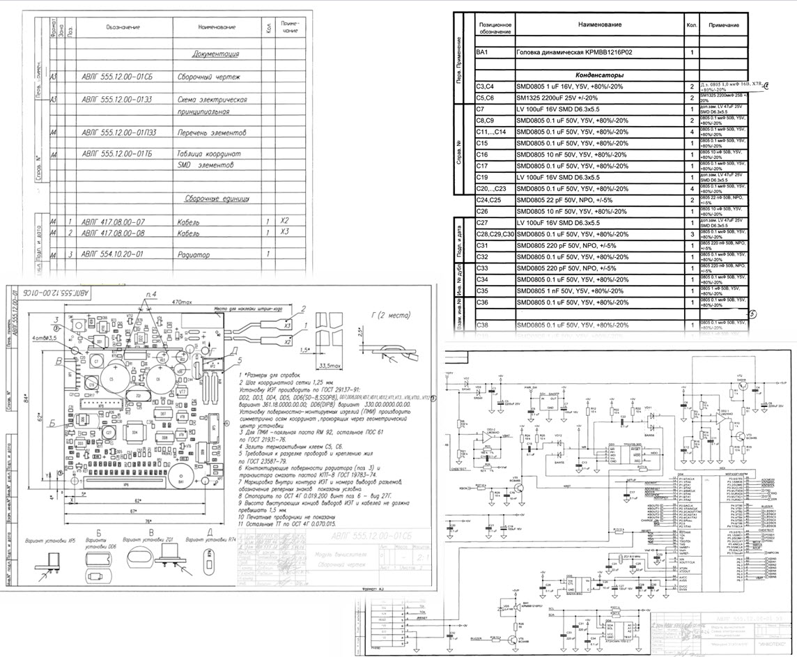
Data on the manufacture of printed circuit boards are formed in a software way and contain the information necessary for the manufacture of photomasks and drilling.
The presentation formats of this data are unified (Gerber, ODB ++) and are de facto standards in transmitting the results to the manufacturer.
Through cycle of computer-aided design of electronic equipment
From the standpoint of users (that is, developers of electronic equipment), CAD REA is a software product whose consumer properties are evaluated according to the following main criteria:
- Support for end-to-end design cycle of electronic equipment by means of automation.
- The functionality of individual subsystems (modeling, trace connections, etc.).
- The openness of the system for its integration with other means of automation in the same or related subject areas.
- High-quality and detailed user documentation.
- Technical support from users of software developers.
In this series of requirements, paramount, as a rule, is the requirement of the possibility of constructing an end-to-end design cycle - from issuing specifications for a project to obtaining design documentation and data for manufacturing a product.
The content of the end-to-end cycle is determined by a set of project stages, consistently performed on the basis of a single information model of the project.
This approach ensures the compatibility of design data and the possibility of iterative product design, that is, the resumption of design work from the initial or one of the intermediate stages with changes in design specifications.
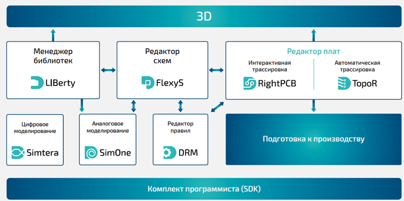
An example of a domestic development CAD system that automates the main stages of electronic device design is the EREMEX software product Delta Design:
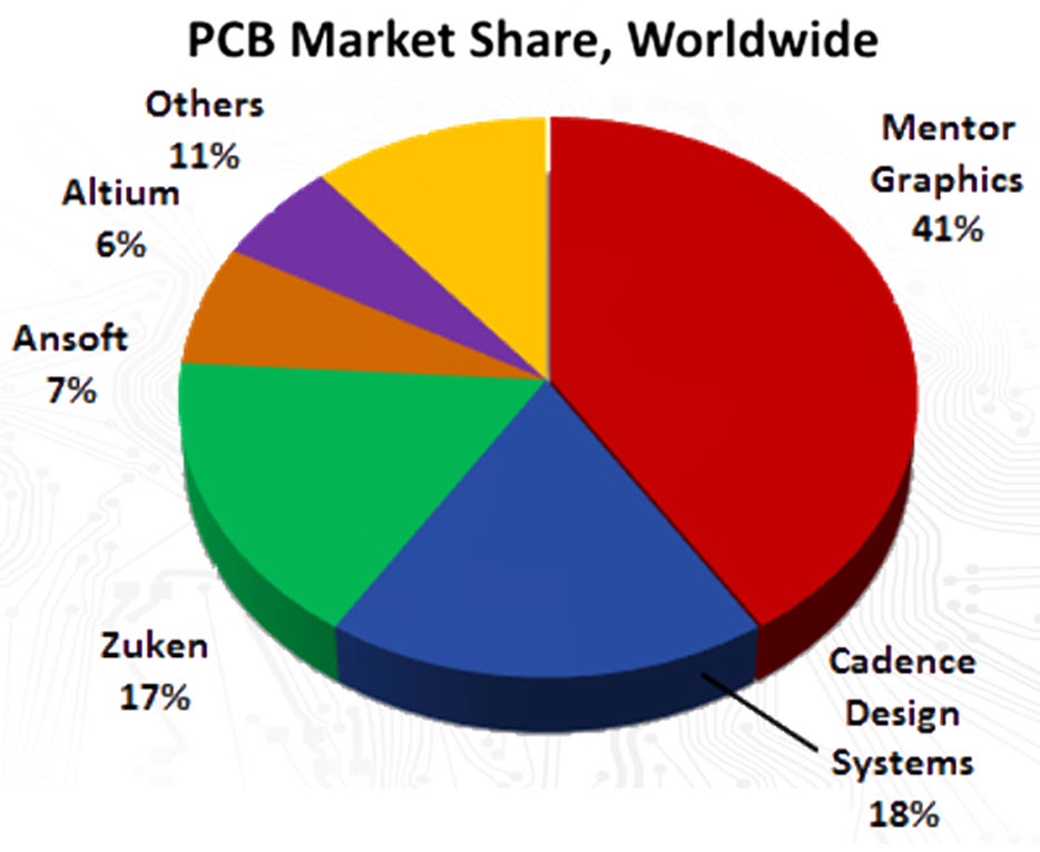 In many cases, electronic equipment companies organize design-through design cycles based on the integration of informational-compatible CAD systems from different manufacturers whose current market is sufficient varied.
Completing the consideration of issues related to the automation of the design of electronic equipment, it should be noted that this area of activity currently continues to develop quite intensively. In the near future, we should expect the emergence of new methods and approaches to solving computer-aided design problems.