VGA graphic controller on SoC without HDL knowledge
- Tutorial
Hello!
In a previous article, my colleague Des333 implemented a framebuffer for an LCD running on an ILI9341 graphics controller . However, writing it required significant experience in developing RTL code.
In addition, not everyone has an embedded LCD-display at hand, but there is certainly a monitor with a VGA-input. What to do if there is little development experience for FPGA, but there is SoC, but you want to do something interesting?
In this article we will tell you how to develop a graphics controller, having on hand a board with SoC (Altera Cyclone V), a display with VGA and minimal knowledge of HDL languages (in our case - Verilog).
For example, we will use our scarves, but everything described will work on others.
Who cares, please, under the cat.
I plan to tell in the following order:
- First, a little about the interaction architecture
- Briefly about connecting to VGA
- How to get firmware using only Quartus Qsys
- How to explain to the kernel that there is a graphics controller. I’ll tell you what needs to be added to dtb and assemble the drivers
- How to get the terminal and X on the display
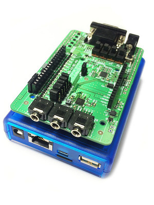
I will use the CB-CV-SOM debug board that works with the CV-SE-SOM SoDIMM module :

We have a shield for this debug board, which has a lot of interesting things besides VGA (see metrotek.spb.ru/cbcvsom. html )
Architecture
To display the image on the display, we need a framebuffer , a driver and a scan module, which will provide a link between the processor and the display, as well as provide continuous frame updates.
In SoC, DDR3 memory (1 GB in our case) is connected to ARM (also called HPS - Hard Processing System), it will contain our framebuffer. And in FPGA there will be a module that we will need to do using Qsys.
Here is the diagram:
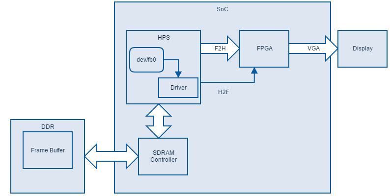
Everything will work like this:
- The driver configures the module in FPGA: after that, the module is ready to receive data from the SDRAM controller and “deploy” it to the display
- In / dev / fb0 write the picture. Data goes to framebuffer in DDR
- FPGA module reads framebuffer continuously and updates screen
How VGA works
VGA (Video Graphics Array) is a video interface that uses an analog signal to transmit color information. The format of the signals and their behavior are similar to a television signal.
Signal list:
vga_vs_o - vertical synchronization
vga_hs_o - horizontal synchronization
vga_r_o - data of the red pixel
component vga_g_o - data of the green pixel
component vga_b_o - data of the blue component of the
Shield pixel supports 16 bits per color, which means that 5 bits are allocated to blue and red, and on green 6. The DAC is made according to the R2R circuit.
Monitors have different resolutions and image refresh rates. These parameters are adjusted in VGA using vertical and horizontal clocks. Which have the following options:
- Clock rate of the appearance of new pixels.
- Front porch - sync pulse blanking time.
- Back porch - rise time of the clock.
- Sync - duration of synchronization.
- Display Area is the point in time when information is transmitted.
The times look like this:

We will use the VGA 800x600 mode at 60 Hz, therefore the following parameters ( parameters for other modes ):
Clock frequency 40 MHz
Horizontal synchronization:
- Front porch 40 pixels
- Back porch 88 pixels
- Sync 128 pixels
- Display Area 800 pixels
Vertical Sync:
- Front porch 1 lines
- Back porch 23 lines
- Sync 4 lines
- Display Area 600 lines
Firmware for FPGA
To get the firmware, we need the following modules in Qsys:
- HPS is our processor.
- Frame Reader - This IP core reads frames stored in external memory and displays them as a video stream.
- Clocked Video Output is an IP core, from Avalon-ST it makes VGA output in a similar format.
- Altera PLL - PLL for changing the clock frequency: we need to get 40 MHz from 25 MHz, which are on the board.
AXI interfaces H2F and F2H come out of the processor, Altera's IP cores have Avalon-ST and Avalon-MM interfaces , therefore, we also need an Interconnect module, which must convert from one interface to another and multiplex data streams. It will appear automatically when files are generated.
More information about Frame Reader and Clocked Video Output can be found here .
How to assemble the firmware and what settings are needed for HPS can be found in this article .
Altera PLL
PLL settings.
Altera PLL
Frame reader
Here are configured:
- FIFO parameters at module input
- Data Transfer Settings
- Number of active pixels
The Bits per pixel per color plane and Number of color planes in parallel parameters are associated with the driver and are explained below. Please note that the dimension of the interface with HPS is the same as the dimension of Master port width .
Frame reader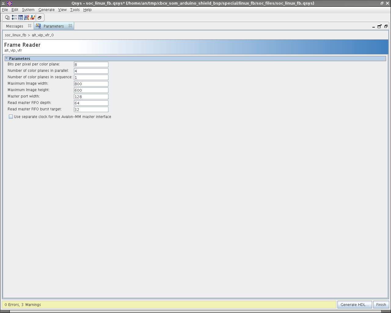
Clocked Video Output
Here:
- Sync settings (vga_vs_o, vga_hs_o), which are described above
- The way the data arrives (it is the same as the Frame Reader)
Clocked Video Output
Qsys Connections
And now we are connecting everything. Settings for the Frame Reader module are “hooked” to h2f master, an interface for transmitting f2h slave data. Connect Clocked Video Output to Frame Reader avalon_streaming_source -> din. Everything is clocked outclk0.
Qsys Connections
And generating files by clicking the Generate the HDL ... .
As mentioned above, the board has 16 bits, and 32 bits come out of the module, so you need to carefully assign pins in the qsf file, or edit the output for yourself in a convenient way in the top file of the project. We need the highest bits of each color, they are more informative than the lower ones.
Please note that this is the first and only place we edit the code. This is no longer required.
logic        vga_v_sync;
logic        vga_h_sync;
logic [31:0] vga_data;
logic [7:0]  vid_r;
logic [7:0]  vid_g;
logic [7:0]  vid_b;
assign  vga_r_o  = vid_r[7:3];
assign  vga_g_o  = vid_g[7:2];
assign  vga_b_o  = vid_b[7:3];
assign  vga_hs_o = vga_h_sync;
assign  vga_vs_o = vga_v_sync;
assign { vid_r, vid_g, vid_b } = vga_data;
Driver and dtb
We will need the altvipfb driver .
Let's go back to the Bits per pixel per color plane and Number of color planes in parallel parameters in Frame Reader . The driver says:
if (bits_per_color != 8) {
          dev_err(&fbdev->pdev->dev,
                  "bits-per-color is set to %i.  Curently only 8 is supported.",
                  bits_per_color);
          return -ENODEV;
}
if (!(fbdev->mem_word_width >= 32 && fbdev->mem_word_width % 32 == 0)) {
          dev_err(&fbdev->pdev->dev,
                  "mem-word-width is set to %i.  must be >= 32 and multiple of 32.",
                  fbdev->mem_word_width);
          return -ENODEV;
         }
The number of bits per color is only 8 and the word width should be greater than or a multiple of 32. What is the reason for this limitation? We look further and see:
/* settings for 32bit pixels */
info->var.red.offset = 16;
info->var.red.length = 8;
info->var.red.msb_right = 0;
info->var.green.offset = 8;
info->var.green.length = 8;
info->var.green.msb_right = 0;
info->var.blue.offset = 0;
info->var.blue.length = 8;
info->var.blue.msb_right = 0;
It becomes clear that the driver works in True color mode , writing color in a 32 bit word (it is more convenient to align than 24), and it works only in this mode.
To build this driver, the following changes must be made in the kernel config.
CONFIG_FB_CFB_FILLRECT=m
CONFIG_FB_CFB_COPYAREA=m
CONFIG_FB_CFB_IMAGEBLIT=m
CONFIG_FB_ALTERA_VIP=m
In order for linux to know that we have a framebuffer from Altera in FPGA, we need to write the following magic words in dtb:
hps_0_h2f: bridge@0xc0000000 {
    compatible = "altr,bridge-1.0", "simple-bus";
    reg = < 0xc0000000 0x20000000 >;
    #address-cells = < 1 >;
    #size-cells = < 1 >;
    ranges = <0x00000000 0xc0000000 0x4080 >;
    alt_vip_vfr_1: vip2@0x0 {
    compatible = "ALTR,vip-frame-reader-13.0", "ALTR,vip-frame-reader-9.1";
    reg = < 0x4000 0x00000080 >;
    max-width = < 800 >; /* MAX_IMAGE_WIDTH type NUMBER */
    max-height = < 600 >; /* MAX_IMAGE_HEIGHT type NUMBER */
    mem-word-width = < 0x80 >;
    bits-per-color = < 0x8 >;
   };
};
In the range parameter , the range of valid addresses from which the driver will read, and in reg = <0x4000 0x00000080> , the start address and how many addresses are occupied by alt_vip. mem-word-width is the Master port width parameter in Frame Reader .
Read more about dtb .
Launch terminal and X
We go to the device and load the driver:
modprobe altvipfb
modprobe fbcon
Then we check whether everything is fine with dmesg, and see if there is a similar line:
[ 66.424283] altvipfb c0000000.vip2: fb0: altvipfb frame buffer device at 0x2c000000+0x12c000
Hooray! Fb0 appeared:
ls -l /dev/fb0
crw-rw---T 1 root fb 29, 0 Nov 26 10:13 /dev/fb0
Then we display the console on the screen connected to the board:
/sbin/getty 38400 tty1
We put icewm and run using startx:
apt-get install icewm icewm-themes
startx
Icewm
Total: we got a graphics controller, with minimal knowledge of HDL languages.