Basics of electrical safety in the design of electronic devices
Hi, Habr!
After the wave raised by my previous post , a rather noticeable number of people asked me (on facebook, in personal account, etc.) what to actually pay attention to, instead of a smart outlet on arduino, not to get another wash-euthanasic .
The topic is large and complex, but I will try to highlight the main points - not least on the basis of errors that I have seen in various real devices and projects, including those published on Habré. I will not be long and tedious to enumerate GOSTs, but I will list quite basic things that must be understood and observed in order not to kill at least yourself (if you plan not to kill others as well, then after completing this article, do not be lazy to go through the relevant GOSTs).
So, you are going to make a device that includes at least one of its ends in the outlet.
Not all devices are equally dangerous - moreover, devices with the same purpose can be more or less dangerous depending on the model of their use. Hazards may include:
Please note that in completely normal living conditions you can get a combination of several factors at once - for example, known cases of killing people with charging smartphones in the bathroom. Firstly, very high humidity with condensation - getting inside the charger, humid air greatly reduces the dielectric strength of the insulation between the primary and secondary circuits, with the result that a breakdown of 230 V to the USB charging connector becomes more than probable (and in Chinese almost guaranteed. Secondly, metal baths and water supply pipes must be grounded to ensure that they do not have life-threatening potentials. Thirdly, the person sitting in the bath has not just a very good electrical contact with her, but a contact that he still cannot get rid of quickly.
Subtract any of these circumstances - and the process of charging your favorite iPhone becomes safe again.
In general, if your device is at least for some signs of a risk zone - it is best not to do it, because understanding how to properly make a device for such conditions is quite trivial and requires relevant experience.
This question seems to be trivial, but most of the crafts fall on it.
The trivial answer: we isolate the circuits which the user can touch (the so-called secondary circuits) from the circuits that are plugged in (the so-called primary circuits).
A slightly less trivial answer to the question of what voltage we are isolated from. On the one hand, we have 230 V rms voltage, total 324 V amplitude - well, let's say, even if as a result of the same zero burnout we get 380 V rms, it will be “only” 536 V amplitude.
However, to make insulation that can withstand 600-800 V is completely inadequate .
The problem is that the network rarely, but aptly, bursts of substantially larger magnitude can occur - moreover, they can be in phase (for example, with a close lightning strike), i.e. induced at the same time in the zero and phase wires. In this case, the voltage “in the socket” will not change significantly with respect to the normal 230 V, but the voltage between the socket and some other “ground” may briefly exceed this 230 V at times.
You should not rely on the short duration of such an impulse - if it breaks through the insulation of your device, a current can flow through the breakdown at a lower voltage. The options here are from simply physical destruction of the insulation to the ignition of the discharge - as in a fluorescent lamp, in which the glow discharge is triggered by a 800-volt pulse from the starter, and then it burns from the usual 230 V AC for an unlimited time.
For this reason, the insulation between the primary and secondary circuits of household appliances is calculated at a voltage of 2.5 kV .
Lyrical digression: you can read about it in great detail, for example, in GOST IEC 60950-1-2014 or GOST IEC 60065-2013referenced by the founding document - Technical Regulations of the Customs Union (ТР ТС) 004/2011 “On the safety of low-voltage equipment”. In particular, both documents indicate for power supply networks with a current voltage up to 300 V possible voltage transients up to 2500 V. According to similar documents, in principle, the whole world lives under the names GOST, IEC or UL 60950.
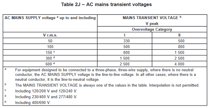
Plate from IEC 60950. In general In the case of calculations relating to user security, the standard recommends that all power mains be categorized as category II.
An important point: the presence of isolation does not mean that current cannot flow between the primary and secondary circuits of the device. In some cases, to avoid such a current is impossible or unreasonable - for example, in pulsed power sources to reduce interference between the primary and secondary cells, there is a small capacitor. In this case, the device should be designed so that the leakage current between the primary and secondary bodies under no circumstances exceeds the safe limit (3.5 mA for household fixed equipment, 0.25-0.75 mA for portable equipment; for medical equipment standards, they are tougher 10-100 times depending on the type of equipment, here you can watch a presentation about the differences in requirements).
So, our minimum requirements are insulation with a strength of 2.5 kV between primary and secondary circuits with leakage current under normal conditions of no more than 3.5 mA.
With the design of printed circuit boards begins, of course, the most interesting. The fact is that “they are designed for voltage not lower” - this is such a phrase about nothing; under actual operating conditions, various factors may play a role, such as the duration of exposure to voltage, the state of the board's surface, the humidity of the air, the presence or absence of moisture condensation ... To deal with them, IEC 60950 introduced various ways of classifying these factors, and the insulation strength is not specified in volts, and in millimeters of the minimum required clearance, taking into account the probability of breakdown of this gap and the consequences to which it will lead. As a result, protection from the same 2.5 kV random throw in the power supply network of category II will look completely different depending on whether the failure of this protection can kill you or not.
Firstly, IEC 60950 introduces four classes of insulation depending on its purpose and, accordingly, the required reliability (more precisely, the probability of failure to multiply by the consequences of this failure):
Further, about the various options for the implementation of the insulation is written quite a lot (IEC standards are paid, but we understand that everything will be found in Yandex ?), We’ll dwell on the requirements for printed circuit boards in home appliances.
To assess the dielectric capacity of various materials, IEC 60950 divides them into groups according to the CTI (Comparative Tracking Index) parameter - the higher the CTI, the better the insulating properties of the material:
Regular glass fiber FR4 has a CTI = 175, that is, belongs to group III, to the boundaries between subgroups IIIa and IIIb.
In addition, the dielectric properties of a material, a discharge in which can occur over its surface (a case of a printed circuit board), depend on the level of contamination of this surface, therefore IEC 60950 introduces several generalized contamination classes (in the standard more formal definitions, below I attach them to operating conditions ):
I note that the required level of protection can be implemented using adequate external enclosures - for example, a device with a level 2 can be used outdoors when using a sealed enclosure.
Finally, IEC 60950 uses two methods for measuring the distance that forms an insulating gap - clearance and creepage.
For our case, for a nominal voltage in the socket of 230 V ± 10%, it is necessary to focus on the requirements for insulation in networks up to 300 V rms voltage, up to 420 V amplitude and up to 2500 V emission during transients.
Depending on the type of insulation (we do not consider the functional, since we are talking about the safety of the user), the minimum required distance on the printed circuit board is:
However, if we return to the above-mentioned Y-capacitor, we can easily notice that the maximum distance between its legs on the datasheet is 7.5 mm.
As it is easy to notice, taking into account the contact pads, it will be difficult for us to get the distance between the conductors of 6.0 mm, if we don’t start to manually pull the legs.
Fortunately, there is a simple way out - as seen in the image above, the creepage can be increased by making a cutout in the PCB. Air has a higher dielectric strength than FR4 - for it, the breakdown voltage approaches 3 kV / mm, and in order to ensure safety, it is usually assumed to be 1-1.5 kV / mm. IEC 60950 requires for an air gap for circuits up to 300 V of width 2.0 mm for basic insulation and 4.0 mm for reinforced (if the production has a quality control program complying with the requirements of the standard, the width can be reduced to 1.5 mm and 3.0 mm, but now this is not our case).
That is, we can provide the necessary insulation with 4 mm air or 6 mm PCB.
Due to the complexity of the issue, the standard does not consider a combinationfrom the air and the printed circuit board, but in practice it is this combination that is used in most cases - a cutout is made between the primary and secondary circuits in the board:
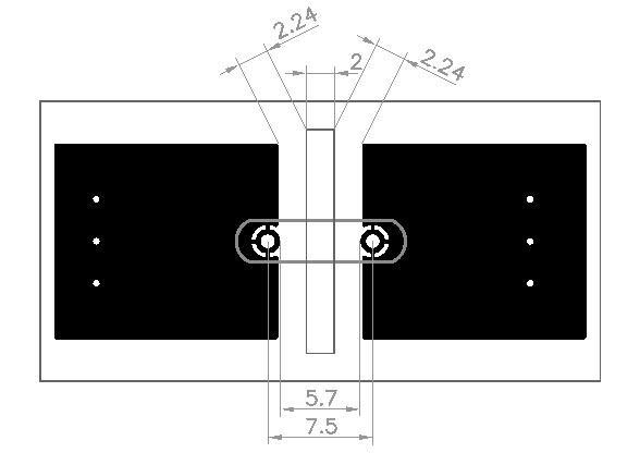
In this case, making a cutout 2 mm wide and slightly longer than the ground fields, we got the minimum creepage equal to 6.48 mm, which satisfies the requirement for reinforced insulation, and across the cut, if you count "head" - 3.7 mm of PCB and 2.0 mm of air, each of the values corresponds to the requirement of one layer of insulation, so that in total can also be considered sufficient.
Here you can live with it.
I note that the correct design of the board does not relieve problems with the location of components: between any conductive parts of the primary and secondary there must be at least the same 2 mm of air, and in the case of an ungrounded enclosure between it and the primary, for reinforced insulation the standard requires 10 mm of air.
PS For the sake of justice, I will add that for reinforced insulation class Y1 capacitors are used, which usually have a distance of 10 mm between the legs. However, this does not negate the need for cuts in PCB where it is not possible to withstand a gap of at least 6 mm for various reasons - due to tight installation, other components with insufficient clearance between the leads, etc. In addition, even if you use Y2-capacitors and guarantee only basic insulation, all the other components, including PCB design, will not be superfluous with safety margin.
In addition, the cuts in the printed circuit board have a few more positive sides - so, dirt does not accumulate on their surface due to the absence of this surface, and they are fine with hygroscopicity. Nevertheless, the presence of cuts in itself does not say anything about the safety of the design, nor their lack of it - about its insecurity.
An obvious fatal mistake is, of course, a complete disregard for safety requirements and maintaining gaps between primary and secondary chains of scale 0.5-1 mm, according to the principle “when you first turned on, you didn't kill anyone - that means everything is in order.” For example, a typical amateur German documentary in which beautiful cuts of functional isolation between the conductors of the power supply are milled, but at the same time there is a millimeter gap between the 230 V input and the secondary ground, on which the USB connector freely accessible to the user sits simply dangerous to life.
In addition to guaranteed fatal errors, potentially fatal errors occur regularly.
First, inexperienced developers are intuitively perceived as high voltage between the two wires of the 230 V network, but not between the primary cell and the secondary, and they lay the cuts between them. This is not unreasonable if the network tracks go on the board close to each other, and this will relate to providing functional isolation, but not directly related to safety - after all, you should have a varistor on between the wires in the standard circuitry the trigger voltage is about 430 V, so there will not be much more there. Moreover, if a high-voltage common-mode pulse arrives to you, then nothing particularly interesting will happen between the wires of the network.
But between the primary and the secondary - how it will happen.
Secondly, the slot in the board by inexperienced developers is perceived as either something decorative, or a silver bullet and a cure for all diseases at once. For example, the same Bitronix Lab laid out pictures of its USB interchange, which they promise to give out to all buyers of a dangerous set for free, and boasted that it was done with a margin of 5 kV:
For simplicity of calculations, I quickly sketch it into DipTrace, the benefit of the component names known, and the size of the slits is easy to calculate from the image - a width of 2 mm, the length does not exceed the width of the components. We do not know how the board is flooded with earth, but we will assume that the polygons do not go beyond the boundaries of the legs of the components.
Total: ADuM4160 - clearance 5.4 mm in PCB + 2 mm air, creepage 2.73 * 2 + 2 = 7.46 mm; AM2D - clearance 4.12 mm PCB + 2 mm air, creepage 6.75 mm. The values are approximate, since the shape of the pads may differ, but ± 0.1 mm we are clearly not worried about here.
It is easy to see that the real parameters only barely exceed the requirements of IEC 60950 for a 300 V network with emissions up to 2500 V for the case of reinforced insulation - and since in the case of the Bitronics Lab we are talking essentially about medical equipment with direct contact with the human body it is desirable to design it under the highest possible level of protection.
The real guaranteed insulation strength of the whole structure will be no higher than 3 kV. Claims about 5 kV with this board are inappropriate under any sauce - it is not designed for this level of protection. In this case, it was possible, without even increasing the size of the printed circuit board, to move the insulator and DC / DC closer to each other and make a single slot under them, extending from the top and bottom beyond the limits of the component housings at least a millimeter.
I note that at high voltages - from 5 kV and above - the shape of the conductors also begins to play a role: the field strength and, accordingly, the probability of breakdown is higher on pointed parts.
Although laboratory tests according to GOST standards for most amateurs are not heavy, for small companies they are unpleasant because of their cost and duration, there are devices on sale that allow a rough assessment of the safety of devices - these are high-voltage insulation resistance meters .
In fact, these are gigo-meters (with an upper limit of 10-20 GOhm), when measuring high voltage applied to probes - 1000 V for low-cost models and 2500 V for those that are more expensive.
If you are engaged in the development of plug-in devices or you are interested in the safety of Chinese products, I highly recommend to purchase at least something like UT-502A (in Chip-and-Dip, too, it is, but expensive).
If your device has sustained 10 seconds under the supplied voltage of 2500 V, then everything is not completely hopeless. Such tests are not grounds for considering the device complying with standards - as it is easy to see, in the general case even a layer of functional insulation is already obliged to withstand such voltages, although the probability of its breakdown is considered too high to be used to protect the user.
Testing equipment with an impulse with a voltage of 5 kV would be more revealing, but, alas, such devices already cost a lot of money.
On the other hand, if even at 2.5 kV your device showed something different from the upper limit of the gigo-meter, you now know what needs to be done with it .
After the wave raised by my previous post , a rather noticeable number of people asked me (on facebook, in personal account, etc.) what to actually pay attention to, instead of a smart outlet on arduino, not to get another wash-euthanasic .
The topic is large and complex, but I will try to highlight the main points - not least on the basis of errors that I have seen in various real devices and projects, including those published on Habré. I will not be long and tedious to enumerate GOSTs, but I will list quite basic things that must be understood and observed in order not to kill at least yourself (if you plan not to kill others as well, then after completing this article, do not be lazy to go through the relevant GOSTs).
So, you are going to make a device that includes at least one of its ends in the outlet.
Determine potential hazard
Not all devices are equally dangerous - moreover, devices with the same purpose can be more or less dangerous depending on the model of their use. Hazards may include:
- The ease of contact of a person with conductive parts - for example, is this contact possible in a living environment or must special actions be taken to achieve it (for example, to get into the electrical panel)
- Qualifications of people for whom the device is intended - it can be children, adult non-professionals or adult professionals. Understanding of the danger of electric shock can be expected only from the latter, from the second - the maximum lack of targeted action on the failure of the device.
- The presence of constant electrical contact with the human body or the possibility of such contact that a person cannot get rid of — the first includes, for example, all medical devices with wearable electrodes, the second — for example, installations in a very limited space in which a person accidentally grasped behind the live electrode, will not be able to free themselves.
- The presence of close to other grounded devices or, on the contrary, devices under voltage — say, the case is earthed near the switchboard, so holding the door with one hand and the other by chance holding the wire under voltage, it is especially easy to go to the forefathers. On the other hand, nonprofessionals should not climb inside the shield at all, and the rest of the grounding of its body protects against the appearance of dangerous voltage on it, for example, if an internal wire breaks inside the shield and accidentally touches the shield body from inside.
- The factors that significantly reduce the breakdown voltage are first of all high humidity, especially with condensation, and secondly lower air pressure (for devices that are used at altitudes above 2000–3000 m, the requirements for the values of protective air gaps between conductive parts begin to grow rapidly ).
Please note that in completely normal living conditions you can get a combination of several factors at once - for example, known cases of killing people with charging smartphones in the bathroom. Firstly, very high humidity with condensation - getting inside the charger, humid air greatly reduces the dielectric strength of the insulation between the primary and secondary circuits, with the result that a breakdown of 230 V to the USB charging connector becomes more than probable (and in Chinese almost guaranteed. Secondly, metal baths and water supply pipes must be grounded to ensure that they do not have life-threatening potentials. Thirdly, the person sitting in the bath has not just a very good electrical contact with her, but a contact that he still cannot get rid of quickly.
Subtract any of these circumstances - and the process of charging your favorite iPhone becomes safe again.
In general, if your device is at least for some signs of a risk zone - it is best not to do it, because understanding how to properly make a device for such conditions is quite trivial and requires relevant experience.
What and from what we isolate?
This question seems to be trivial, but most of the crafts fall on it.
The trivial answer: we isolate the circuits which the user can touch (the so-called secondary circuits) from the circuits that are plugged in (the so-called primary circuits).
A slightly less trivial answer to the question of what voltage we are isolated from. On the one hand, we have 230 V rms voltage, total 324 V amplitude - well, let's say, even if as a result of the same zero burnout we get 380 V rms, it will be “only” 536 V amplitude.
However, to make insulation that can withstand 600-800 V is completely inadequate .
The problem is that the network rarely, but aptly, bursts of substantially larger magnitude can occur - moreover, they can be in phase (for example, with a close lightning strike), i.e. induced at the same time in the zero and phase wires. In this case, the voltage “in the socket” will not change significantly with respect to the normal 230 V, but the voltage between the socket and some other “ground” may briefly exceed this 230 V at times.
You should not rely on the short duration of such an impulse - if it breaks through the insulation of your device, a current can flow through the breakdown at a lower voltage. The options here are from simply physical destruction of the insulation to the ignition of the discharge - as in a fluorescent lamp, in which the glow discharge is triggered by a 800-volt pulse from the starter, and then it burns from the usual 230 V AC for an unlimited time.
For this reason, the insulation between the primary and secondary circuits of household appliances is calculated at a voltage of 2.5 kV .
Lyrical digression: you can read about it in great detail, for example, in GOST IEC 60950-1-2014 or GOST IEC 60065-2013referenced by the founding document - Technical Regulations of the Customs Union (ТР ТС) 004/2011 “On the safety of low-voltage equipment”. In particular, both documents indicate for power supply networks with a current voltage up to 300 V possible voltage transients up to 2500 V. According to similar documents, in principle, the whole world lives under the names GOST, IEC or UL 60950.
Plate from IEC 60950. In general In the case of calculations relating to user security, the standard recommends that all power mains be categorized as category II.
An important point: the presence of isolation does not mean that current cannot flow between the primary and secondary circuits of the device. In some cases, to avoid such a current is impossible or unreasonable - for example, in pulsed power sources to reduce interference between the primary and secondary cells, there is a small capacitor. In this case, the device should be designed so that the leakage current between the primary and secondary bodies under no circumstances exceeds the safe limit (3.5 mA for household fixed equipment, 0.25-0.75 mA for portable equipment; for medical equipment standards, they are tougher 10-100 times depending on the type of equipment, here you can watch a presentation about the differences in requirements).
So, our minimum requirements are insulation with a strength of 2.5 kV between primary and secondary circuits with leakage current under normal conditions of no more than 3.5 mA.
How do we isolate it?
- All components connecting the primary and secondary circuits must be designed for an insulation voltage of at least 2.5 kV. In a pulsed power supply, this is usually a transformer, a feedback optocoupler and a noise suppressor capacitor.
- There should be no direct connections between the primary and secondary circuits.
- Interference-canceling capacitors connecting the primary and secondary circuits must be officially certified to a class not lower than Y2 ( safety rated Y2 capacitors ) - such and only such capacitors can be used in circuits where the output of the capacitor fails. Capacitors of class Y2 are marked in the current voltage of the AC network for which they are designed ("250VAC"), while they are guaranteed resistance to single pulses with voltage up to 5 kV. No other capacitors, including those marked 3 kV or higher, but not having a safety class, should not be used in such circuits . Typical example - Murata capacitors of the DE2 series.. For reinforced insulation (see below) class Y1 capacitors should be used, for example, Murata DE1 .
- When designing a printed circuit board, the gaps between conductors, parts and the device case must be designed for a breakdown voltage of at least 2.5 kV.
With the design of printed circuit boards begins, of course, the most interesting. The fact is that “they are designed for voltage not lower” - this is such a phrase about nothing; under actual operating conditions, various factors may play a role, such as the duration of exposure to voltage, the state of the board's surface, the humidity of the air, the presence or absence of moisture condensation ... To deal with them, IEC 60950 introduced various ways of classifying these factors, and the insulation strength is not specified in volts, and in millimeters of the minimum required clearance, taking into account the probability of breakdown of this gap and the consequences to which it will lead. As a result, protection from the same 2.5 kV random throw in the power supply network of category II will look completely different depending on whether the failure of this protection can kill you or not.
Firstly, IEC 60950 introduces four classes of insulation depending on its purpose and, accordingly, the required reliability (more precisely, the probability of failure to multiply by the consequences of this failure):
- Functional - necessary for the operation of the device itself, but not providing user protection.
- Basic - providing an initial level of user protection, but not reliable enough to do without a second protective barrier.
- Supplementary - the second protective barrier. It has the same strength as the Basic.
- Reinforced is a high-strength insulation that can be used without a second protective barrier. It is twice as strong as Basic.
Further, about the various options for the implementation of the insulation is written quite a lot (IEC standards are paid, but we understand that everything will be found in Yandex ?), We’ll dwell on the requirements for printed circuit boards in home appliances.
To assess the dielectric capacity of various materials, IEC 60950 divides them into groups according to the CTI (Comparative Tracking Index) parameter - the higher the CTI, the better the insulating properties of the material:
- Group IIIb - 100 <CTI <175
- Group IIIa - 175 <CTI <400
- Group II - 400 <CTI <600
- Group I - CTI> 600
Regular glass fiber FR4 has a CTI = 175, that is, belongs to group III, to the boundaries between subgroups IIIa and IIIb.
In addition, the dielectric properties of a material, a discharge in which can occur over its surface (a case of a printed circuit board), depend on the level of contamination of this surface, therefore IEC 60950 introduces several generalized contamination classes (in the standard more formal definitions, below I attach them to operating conditions ):
- Level I - pollution that does not degrade the dielectric strength of the insulation. Applies only to equipment in clean rooms or in sealed enclosures that prevent ingress even household pollutants.
- Level 2 - office or home environment, possible pollutants usually do not conduct current, but in isolated cases with moisture condensation can become conductive.
- Level 3 - industrial environment, agricultural enterprises, especially unheated premises. Contaminants can conduct current, as in the case of condensate, and without it.
- Level 4 - use without protection from the external environment, regular exposure to water or snow.
I note that the required level of protection can be implemented using adequate external enclosures - for example, a device with a level 2 can be used outdoors when using a sealed enclosure.
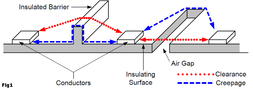
Finally, IEC 60950 uses two methods for measuring the distance that forms an insulating gap - clearance and creepage.
- Clearance - the shortest distance between the conductors.
- Creepage - the distance between the conductors on the surface of the printed circuit board.
For our case, for a nominal voltage in the socket of 230 V ± 10%, it is necessary to focus on the requirements for insulation in networks up to 300 V rms voltage, up to 420 V amplitude and up to 2500 V emission during transients.
Depending on the type of insulation (we do not consider the functional, since we are talking about the safety of the user), the minimum required distance on the printed circuit board is:
- Basic: 3.0 mm if device has extra insulation
- Reinforced: 6.0 mm, if the device does not have additional insulation
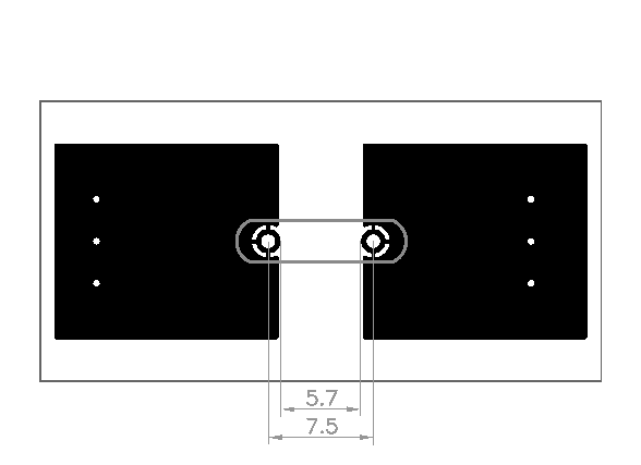
However, if we return to the above-mentioned Y-capacitor, we can easily notice that the maximum distance between its legs on the datasheet is 7.5 mm.
As it is easy to notice, taking into account the contact pads, it will be difficult for us to get the distance between the conductors of 6.0 mm, if we don’t start to manually pull the legs.
Fortunately, there is a simple way out - as seen in the image above, the creepage can be increased by making a cutout in the PCB. Air has a higher dielectric strength than FR4 - for it, the breakdown voltage approaches 3 kV / mm, and in order to ensure safety, it is usually assumed to be 1-1.5 kV / mm. IEC 60950 requires for an air gap for circuits up to 300 V of width 2.0 mm for basic insulation and 4.0 mm for reinforced (if the production has a quality control program complying with the requirements of the standard, the width can be reduced to 1.5 mm and 3.0 mm, but now this is not our case).
That is, we can provide the necessary insulation with 4 mm air or 6 mm PCB.
Due to the complexity of the issue, the standard does not consider a combinationfrom the air and the printed circuit board, but in practice it is this combination that is used in most cases - a cutout is made between the primary and secondary circuits in the board:
In this case, making a cutout 2 mm wide and slightly longer than the ground fields, we got the minimum creepage equal to 6.48 mm, which satisfies the requirement for reinforced insulation, and across the cut, if you count "head" - 3.7 mm of PCB and 2.0 mm of air, each of the values corresponds to the requirement of one layer of insulation, so that in total can also be considered sufficient.
Here you can live with it.
I note that the correct design of the board does not relieve problems with the location of components: between any conductive parts of the primary and secondary there must be at least the same 2 mm of air, and in the case of an ungrounded enclosure between it and the primary, for reinforced insulation the standard requires 10 mm of air.
PS For the sake of justice, I will add that for reinforced insulation class Y1 capacitors are used, which usually have a distance of 10 mm between the legs. However, this does not negate the need for cuts in PCB where it is not possible to withstand a gap of at least 6 mm for various reasons - due to tight installation, other components with insufficient clearance between the leads, etc. In addition, even if you use Y2-capacitors and guarantee only basic insulation, all the other components, including PCB design, will not be superfluous with safety margin.
In addition, the cuts in the printed circuit board have a few more positive sides - so, dirt does not accumulate on their surface due to the absence of this surface, and they are fine with hygroscopicity. Nevertheless, the presence of cuts in itself does not say anything about the safety of the design, nor their lack of it - about its insecurity.
Classic mistakes
An obvious fatal mistake is, of course, a complete disregard for safety requirements and maintaining gaps between primary and secondary chains of scale 0.5-1 mm, according to the principle “when you first turned on, you didn't kill anyone - that means everything is in order.” For example, a typical amateur German documentary in which beautiful cuts of functional isolation between the conductors of the power supply are milled, but at the same time there is a millimeter gap between the 230 V input and the secondary ground, on which the USB connector freely accessible to the user sits simply dangerous to life.
In addition to guaranteed fatal errors, potentially fatal errors occur regularly.
First, inexperienced developers are intuitively perceived as high voltage between the two wires of the 230 V network, but not between the primary cell and the secondary, and they lay the cuts between them. This is not unreasonable if the network tracks go on the board close to each other, and this will relate to providing functional isolation, but not directly related to safety - after all, you should have a varistor on between the wires in the standard circuitry the trigger voltage is about 430 V, so there will not be much more there. Moreover, if a high-voltage common-mode pulse arrives to you, then nothing particularly interesting will happen between the wires of the network.
But between the primary and the secondary - how it will happen.
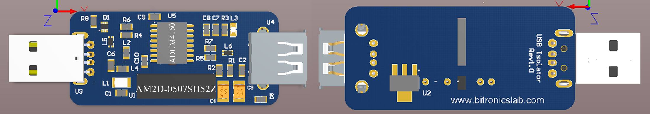
Secondly, the slot in the board by inexperienced developers is perceived as either something decorative, or a silver bullet and a cure for all diseases at once. For example, the same Bitronix Lab laid out pictures of its USB interchange, which they promise to give out to all buyers of a dangerous set for free, and boasted that it was done with a margin of 5 kV:
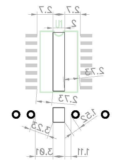
For simplicity of calculations, I quickly sketch it into DipTrace, the benefit of the component names known, and the size of the slits is easy to calculate from the image - a width of 2 mm, the length does not exceed the width of the components. We do not know how the board is flooded with earth, but we will assume that the polygons do not go beyond the boundaries of the legs of the components.
Total: ADuM4160 - clearance 5.4 mm in PCB + 2 mm air, creepage 2.73 * 2 + 2 = 7.46 mm; AM2D - clearance 4.12 mm PCB + 2 mm air, creepage 6.75 mm. The values are approximate, since the shape of the pads may differ, but ± 0.1 mm we are clearly not worried about here.
It is easy to see that the real parameters only barely exceed the requirements of IEC 60950 for a 300 V network with emissions up to 2500 V for the case of reinforced insulation - and since in the case of the Bitronics Lab we are talking essentially about medical equipment with direct contact with the human body it is desirable to design it under the highest possible level of protection.
The real guaranteed insulation strength of the whole structure will be no higher than 3 kV. Claims about 5 kV with this board are inappropriate under any sauce - it is not designed for this level of protection. In this case, it was possible, without even increasing the size of the printed circuit board, to move the insulator and DC / DC closer to each other and make a single slot under them, extending from the top and bottom beyond the limits of the component housings at least a millimeter.
I note that at high voltages - from 5 kV and above - the shape of the conductors also begins to play a role: the field strength and, accordingly, the probability of breakdown is higher on pointed parts.
How to check an existing device?
Although laboratory tests according to GOST standards for most amateurs are not heavy, for small companies they are unpleasant because of their cost and duration, there are devices on sale that allow a rough assessment of the safety of devices - these are high-voltage insulation resistance meters .
In fact, these are gigo-meters (with an upper limit of 10-20 GOhm), when measuring high voltage applied to probes - 1000 V for low-cost models and 2500 V for those that are more expensive.
If you are engaged in the development of plug-in devices or you are interested in the safety of Chinese products, I highly recommend to purchase at least something like UT-502A (in Chip-and-Dip, too, it is, but expensive).
If your device has sustained 10 seconds under the supplied voltage of 2500 V, then everything is not completely hopeless. Such tests are not grounds for considering the device complying with standards - as it is easy to see, in the general case even a layer of functional insulation is already obliged to withstand such voltages, although the probability of its breakdown is considered too high to be used to protect the user.
Testing equipment with an impulse with a voltage of 5 kV would be more revealing, but, alas, such devices already cost a lot of money.
On the other hand, if even at 2.5 kV your device showed something different from the upper limit of the gigo-meter, you now know what needs to be done with it .