Briefly about the architecture of neuromorphic processors: a view from the inside
Researchers from IBM have published a patent application with the structure of the neuromorphic chips TrueNorth. We decided to take a look at this document and explain how the IBM processor works.

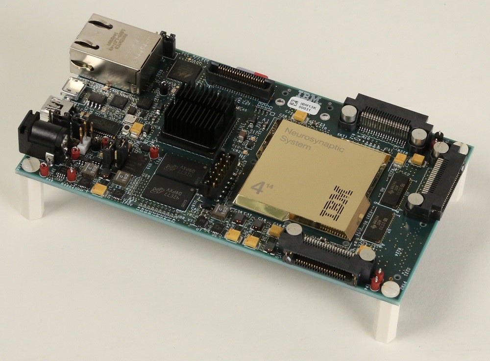
/ Flickr / IBM Research / CC
TrueNorth is a neuromorphic processor developed in 2014 by IBM with the support of DARPA. The term “neuromorphic” means that the architecture of the chip is based on the principles of the human brain.
Such a device emulates the work of millions of neurons with processes - dendrites and axons . The first are responsible for the perception of information, and the second - for its transmission. At the same time, all neurons are interconnected by synapses - special contacts that transmit electrical signals (nerve impulses).
According to IBM developers, the TrueNorth task is to accelerate neural network learning. Neuromorphic processors, unlike classical ones, do not need to access memory (or registers) each time and extract data from there - all information is already stored in artificial neurons.
TrueNorth is made on 28-nanometer process technology. The processor contains 5.4 billion transistors and 4096 cores. Each core was provided with a task scheduler, SRAM-memory and a router. This structure allowed us to simulate the work of a million neurons and 256 million synapses.
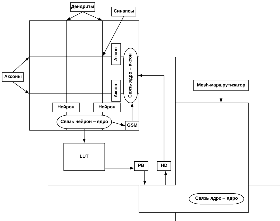
In its patent , IBM cites the following scheme:

The principles of the chip can be represented by the example of convolutional neural networks for image recognition. The processor is a layer of neurons. When a neuron identifies data, such as a shape outline, a pulse is generated. Each such pulse, conditionally, denotes one pixel of the image.
Further, the first layer of neurons transmits data to the next layer (through all the same pulses). Thus, layer by layer, the network recognizes an image — first, the outlines and details, and then the whole picture.
Regular languages are not suitable for programming neurosynaptic nuclei. Therefore, IBM developedspecial language corelet. It has the basic properties of OOP: encapsulation, inheritance and polymorphism and is based on MATLAB. With it, the kernel is defined as classes, in order to manage their work was easier. The developers gave an example of code in their presentation ( p. 17 ).
Above neuromorphic processors work not only at IBM. Intel has been developing a Loihi chip since 2017 . It consists of 130 thousand artificial neurons and 130 million synapses. This year, the IT giant has completed the production of an experimental sample of the 14-nm process technology. According to the results of the first tests, the chip recognizes 3D data from different angles, for a couple of seconds it learns a set of data for training.
Another similar project is being developed by Brainchip. Their Akida system contains 1.2 million neurons and 10 billion synapses. The processor is equipped with interfaces for image recognition, audio data and analog signals. Scheme of the system is presented on the project website .
Such technologies are designed to accelerate the training of convolutional neural networks , “sharpened” under the image recognition. For example, in 2017, researchers tested TrueNorth and a DVS-camera (Dynamic Vision Sensor), the principle of which resembles the work of the retina. The neural network recognized ten gestures with an accuracy of 96.5%.
In addition, based on the processor will create a system of cyber defense. Researchers from IBM have already proposed the concept of True Cyber Security solution, which detects intrusions into the computer network in 90% of cases (80% of them determine the type of attack).
As conceived by the developers of neural processors, MO systems based on this technology will not have to constantly connect to the network for training, since all the algorithms will be implemented locally. This property will allow the use of the chip in smartphones, data centers and smart devices based on AI systems.
Researchers have yet to develop solutions that make it easy to program a chip to perform specific tasks. Specialized PL is only the first step for the development of the entire ecosystem. Because of the large-scale implementation of technology in user devices can not speak.
PS We have a Telegram channel - there we write about virtualization technologies and IaaS:

/ Flickr / IBM Research / CC
About project TrueNorth
TrueNorth is a neuromorphic processor developed in 2014 by IBM with the support of DARPA. The term “neuromorphic” means that the architecture of the chip is based on the principles of the human brain.
Such a device emulates the work of millions of neurons with processes - dendrites and axons . The first are responsible for the perception of information, and the second - for its transmission. At the same time, all neurons are interconnected by synapses - special contacts that transmit electrical signals (nerve impulses).
According to IBM developers, the TrueNorth task is to accelerate neural network learning. Neuromorphic processors, unlike classical ones, do not need to access memory (or registers) each time and extract data from there - all information is already stored in artificial neurons.
What does the chip look like from the inside?
TrueNorth is made on 28-nanometer process technology. The processor contains 5.4 billion transistors and 4096 cores. Each core was provided with a task scheduler, SRAM-memory and a router. This structure allowed us to simulate the work of a million neurons and 256 million synapses.
In its patent , IBM cites the following scheme:

The principles of the chip can be represented by the example of convolutional neural networks for image recognition. The processor is a layer of neurons. When a neuron identifies data, such as a shape outline, a pulse is generated. Each such pulse, conditionally, denotes one pixel of the image.
Further, the first layer of neurons transmits data to the next layer (through all the same pulses). Thus, layer by layer, the network recognizes an image — first, the outlines and details, and then the whole picture.
Regular languages are not suitable for programming neurosynaptic nuclei. Therefore, IBM developedspecial language corelet. It has the basic properties of OOP: encapsulation, inheritance and polymorphism and is based on MATLAB. With it, the kernel is defined as classes, in order to manage their work was easier. The developers gave an example of code in their presentation ( p. 17 ).
Similar solutions
Above neuromorphic processors work not only at IBM. Intel has been developing a Loihi chip since 2017 . It consists of 130 thousand artificial neurons and 130 million synapses. This year, the IT giant has completed the production of an experimental sample of the 14-nm process technology. According to the results of the first tests, the chip recognizes 3D data from different angles, for a couple of seconds it learns a set of data for training.
Another similar project is being developed by Brainchip. Their Akida system contains 1.2 million neurons and 10 billion synapses. The processor is equipped with interfaces for image recognition, audio data and analog signals. Scheme of the system is presented on the project website .
For what tasks neurochips are suitable
Such technologies are designed to accelerate the training of convolutional neural networks , “sharpened” under the image recognition. For example, in 2017, researchers tested TrueNorth and a DVS-camera (Dynamic Vision Sensor), the principle of which resembles the work of the retina. The neural network recognized ten gestures with an accuracy of 96.5%.
In addition, based on the processor will create a system of cyber defense. Researchers from IBM have already proposed the concept of True Cyber Security solution, which detects intrusions into the computer network in 90% of cases (80% of them determine the type of attack).
As conceived by the developers of neural processors, MO systems based on this technology will not have to constantly connect to the network for training, since all the algorithms will be implemented locally. This property will allow the use of the chip in smartphones, data centers and smart devices based on AI systems.
Researchers have yet to develop solutions that make it easy to program a chip to perform specific tasks. Specialized PL is only the first step for the development of the entire ecosystem. Because of the large-scale implementation of technology in user devices can not speak.
PS We have a Telegram channel - there we write about virtualization technologies and IaaS:
