Adjustable power supply from ATX power supply to TL494. Part 1 - iron
Hello!
Today I would like to tell you about my experience of converting the most common Chinese ATX PSU into a regulated power supply with current and voltage stabilization (0-20A, 0-24V).
In this article we will take a closer look at the operation of the TL494 PWM controller, feedback and go over the modernization of the power supply circuit and the development of a homemade board of error and current error amplifiers.
Honestly, now I can not even name the model of the experimental PSU. One of the many cheap 300W P4 ready. I hope you don’t need to be reminded that in reality this 300W means no more than 150, and then with the appearance of the smell of roast in the apartment.
I expect that my experience will be useful to someone from a practical point of view, and therefore I will focus on theory. Without it, it will still not be possible to remake the BP. in any case there will be some differences in the scheme and complexity during the adjustment.
ATX power supply circuit
To begin, let's go through the ATX power supply circuit on the TL494 controller (and its numerous clones).
All schemes are very similar to each other. Google gives them out quite a lot and it seems I found it almost corresponding to my copy.
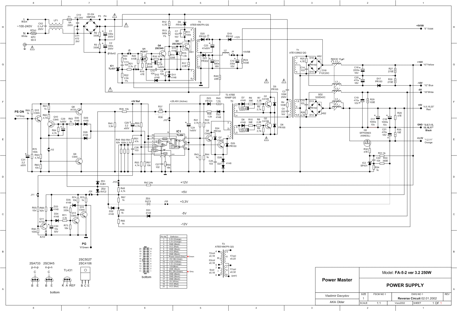
Full size link to the diagram
Structurally, we divide the power supply unit into the following units:
- mains voltage rectifier with filter
- standby power supply (+ 5V standby)
- main power supply (+ 12V, -12V, + 3.3V, + 5V, -5V)
- control circuit of the main voltages, generation PowerGood signal and short-circuit protection
Rectifier with filters is all that is in the upper left corner of the circuit to the diodes D1-D4.
The source of standby power is assembled on the transformer T3 and transistors Q3 Q4. Stabilization is based on feedback through the U1 optocoupler and the TL431 reference voltage source. I will not consider in detail the work of this part. I know that too long articles are not very fun to read. At the end I will give the name of the book, where all the details are discussed in detail.
Please note that in the circuit by mistake, the TL494 PWM controller and the TL431 stand-by power ion source are designated as IC1. In the future, I will mention IC1 meaning precisely the PWM controller.
The main power source is assembled on the transformer T1, high-voltage switches Q1 Q2, control transformer T2 and low-voltage switches Q6 Q7. The whole thing is swinging and controlled by the IC1 PWM chip. Understanding the principle of operation of the controller and the purpose of each element of its strapping is just what is needed for the conscious refinement of the BP instead of blindly repeating other people's recommendations and schemes.
The mechanism of operation is approximately as follows: the PWM controller, alternately opening the low-voltage switches Q6 Q7, creates an EMF in the primary winding of the T2 transformer. See, these keys are powered by low voltage from a standby power source? Find on the diagram R46 and understand what I mean. The PWM controller is also powered by this duty voltage. Just above, I called the transformer T2 a control, but it seems that it has some more correct name. Its main task is the galvanic isolation of the low-voltage and high-voltage parts of the circuit. The secondary windings of this transformer control the high-voltage switches Q1 Q2, alternately opening them. With this trick, low-voltage PWM controller can control high-voltage switches in compliance with safety measures. The high-voltage switches Q1 Q2, in turn, swing the primary winding of the T1 transformer and the main voltages of interest arise on its secondary windings. High-voltage, these keys are called because they commute rectified mains voltage, and it is about 300V! The voltage from the secondary windings T1 is rectified and filtered using LC filters.
Now, I hope, the whole picture you imagine and we can go on.
PWM controller TL494.
Let's see how the PWM controller TL494 works.
It would be better if you download the datasheet www.ti.com/lit/ds/symlink/tl494.pdf , but in principle I will try to extract from it the most important thing with the help of pictures. For a deeper understanding of all the subtleties I advise this document: www.ti.com/lit/an/slva001e/slva001e.pdf
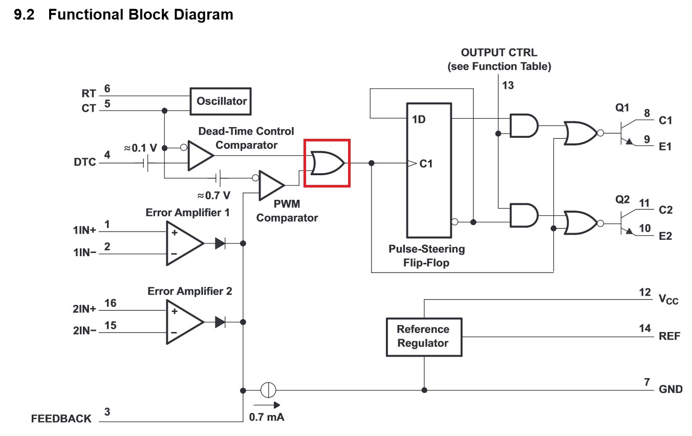
We begin, oddly enough, from the end - with the output part of the chip.
Now all the attention to the output element OR (marked with a red square).
The output of this element at a specific point in time directly controls the state of one or both keys Q1 Q2.
The control option is set via pin 13 (Output control).
Important thing number 1: if the output element OR log 1 - output keys are closed (turned off). This is true for both modes.
Important thing number 2: if the output element OR log 0 - one of the keys (or both at once) is open (enabled).
The following picture emerges: on the rising front, the previously opened transistor closes (at this moment both of them are guaranteed to be closed), the trigger changes its state and on the descending front another key is turned on and will remain on until the rising edge comes again and closes it, The moment the trigger is again fliped over and the next descending front will open another transistor. In single ended mode, the keys always work synchronously and the trigger is not used.
The time when the output is in the log. 1 (and both keys are locked) is called Dead time.
The ratio of the pulse duration (log. 0, the transistor is open) to the period of their repetition is called the duty cycle (PWM duty cycle). For example, if the ratio is 100%, then the output element OR is always 0 and the transistor (or both) is always open.
Sorry, but I try to explain as much as possible and almost on my fingers, because this can be read in an official dry language and in a datasheet.
Oh yeah, why do we need Dead time? In short: in real life, the top key will pull up (to plus) and the bottom down (to minus). If you open them simultaneously - there will be a short circuit. This is called through current and because of parasitic capacitances, inductances and other features such a mode arises even if you open the keys strictly in turn. To minimize the through current, dead time is needed.
Now let's pay attention to the saw generator (oscillator), which uses pins 5 and 6 of the chip to set the frequency.
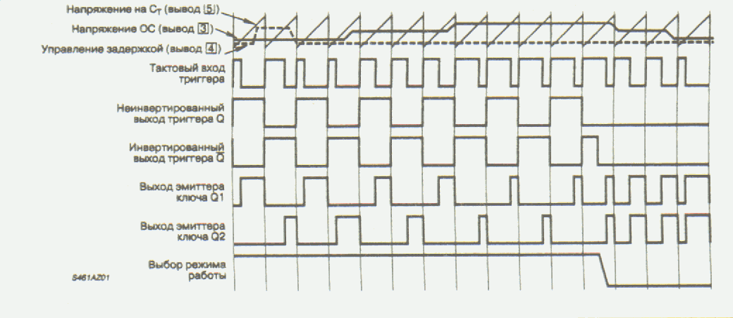
A resistor and a capacitor are connected to these pins. This is the very RC generator about which probably many have heard. Now at pin 5 (CT) we saw from 0 to 3.3V. As you can see, this saw is fed to the inverting inputs of the Comparators Dead-time and PWM.
The terms and the work of the output part of the PWM controller are more or less defined, now we will deal with what it saw and why do we need all these comparators and error amplifiers. We realized that the ratio of the pulse duration to the period of their sequence determines the fill factor, and hence the output voltage of the power source because The more energy is pumped into the primary winding of the transformer, the greater the fill factor.
For example, let's look at what needs to be done to set the fill factor to 50%. Do you still remember about the saw? It is fed to the inverting inputs of the PWM and Dead time comparators. It is known that if the voltage on the inverting input is higher than on the non-inverting input - the comparator output will be log.0. Let me remind you that the saw is a signal that rises smoothly from 0 to 3.3v, after which it drops sharply to 0v.
Thus, at the output of the comparator 50% of the time there was a log.0 — half of the saw voltage must be supplied to the non-inverting input (3.3V / 2 = 1.65V). This will give the desired 50% duty cycle.
We noticed that both comparators converge on the very same OR element, which means that as long as one of the comparators issues log.1, the other cannot prevent it. Those. priority is the comparator, which leads to a lower fill factor. And if the dead time comparator voltage is supplied from the outside, then on the PWM comparator, you can send a signal both from the outside (3 pins) and from the built-in error amplifiers (these are ordinary opamps). They are also connected according to the scheme OR, but since we are already dealing with an analog signal - the OR circuit is implemented using diodes. Thus, the control over the fill factor captures that error amplifier, which asks for a smaller fill factor. The state of the other does not matter.
Feedback.
Well, now how to build a power source on all this? Very simple! It is necessary to cover BP with negative feedback. The difference between the desired (specified) and the available voltage is called an error. If at each moment of time we influence the fill factor so as to correct the error and bring it to 0, we obtain stabilization of the output voltage (or current). Feedback is negative as long as the control action responds to an error with the opposite sign. If the feedback is positive - write is gone! In this case, the feedback will increase the error instead of reducing it.
All this work for those very error amplifiers. A reference voltage (standard) is applied to the inverting input of the error amplifier, and a voltage is applied to the non-inverting input power supply. By the way, inside the PWM controller there is a 5V reference voltage source, which is a reference point in all dimensions.
Compensation feedback
I don’t even know how to explain this in a simpler way. With feedback, everything is simple only in an ideal world. In practice, if you change the fill factor - the output voltage does not change immediately, but with some delay.
For example, the error amplifier registered a voltage drop at the output, corrected the fill factor and stopped interfering with the system, but the voltage continues to increase and then the error amplifier is forced to adjust the fill factor again in the other direction. This situation is due to a delayed reaction. So the system can go into oscillation mode. They are fading and not fading. A power supply unit in which persistent oscillations of the feedback signal may occur will not last long and is unstable.
Feedback has a certain bandwidth. Suppose 100kHz band. This means that if the output voltage oscillates with a frequency higher than 100 kHz, the feedback will simply not notice this and nothing will be corrected. Of course, we would like the feedback to respond to changes in any frequency and the output voltage was as stable as possible. Those. the struggle is to ensure that the feedback is as broadband as possible. However, the very delayed reaction will not allow us to make the band infinitely wide. And if the bandwidth of the feedback circuit is wider than the capacity of the BP itself to test the control signals (direct link) - at some frequencies the negative feedback will suddenly become positive and instead of compensating for the error it will further increase,
Now, from delays in seconds, let's move on to frequencies, gains and phase shifts ...
The bandwidth is the maximum frequency at which the gain is greater than 1.
As the frequency increases, the gain decreases. In principle, this is true for any amplifier.
So, in order for our PSU to work stably, one condition must be met: in the entire frequency band, where the total gain of the forward and feedback link is greater than 1 (0 dB), the phase lag should not exceed 310 degrees. 180 degrees makes the inverting input of the error amplifier.
By entering feedback, various filters ensure that this rule is fulfilled. If it is very rough, then the feedback compensation is the adjustment of the bandwidth and the frequency response of the feedback for the reactions of a real power source (for the characteristics of a direct connection).
This topic is not very simple, under it lies a pile of mathematics, research and other works ... I just try to state the essence of the issue in an accessible form. I can recommend to read this article, where, although not so on the fingers, but this question is also presented in an accessible form and references to the literature are given: bsvi.ru/kompensaciya-obratnoj-svyazi-v-impulsnyx-istochnikax-pitaniya-chast- 1
From theory to practice
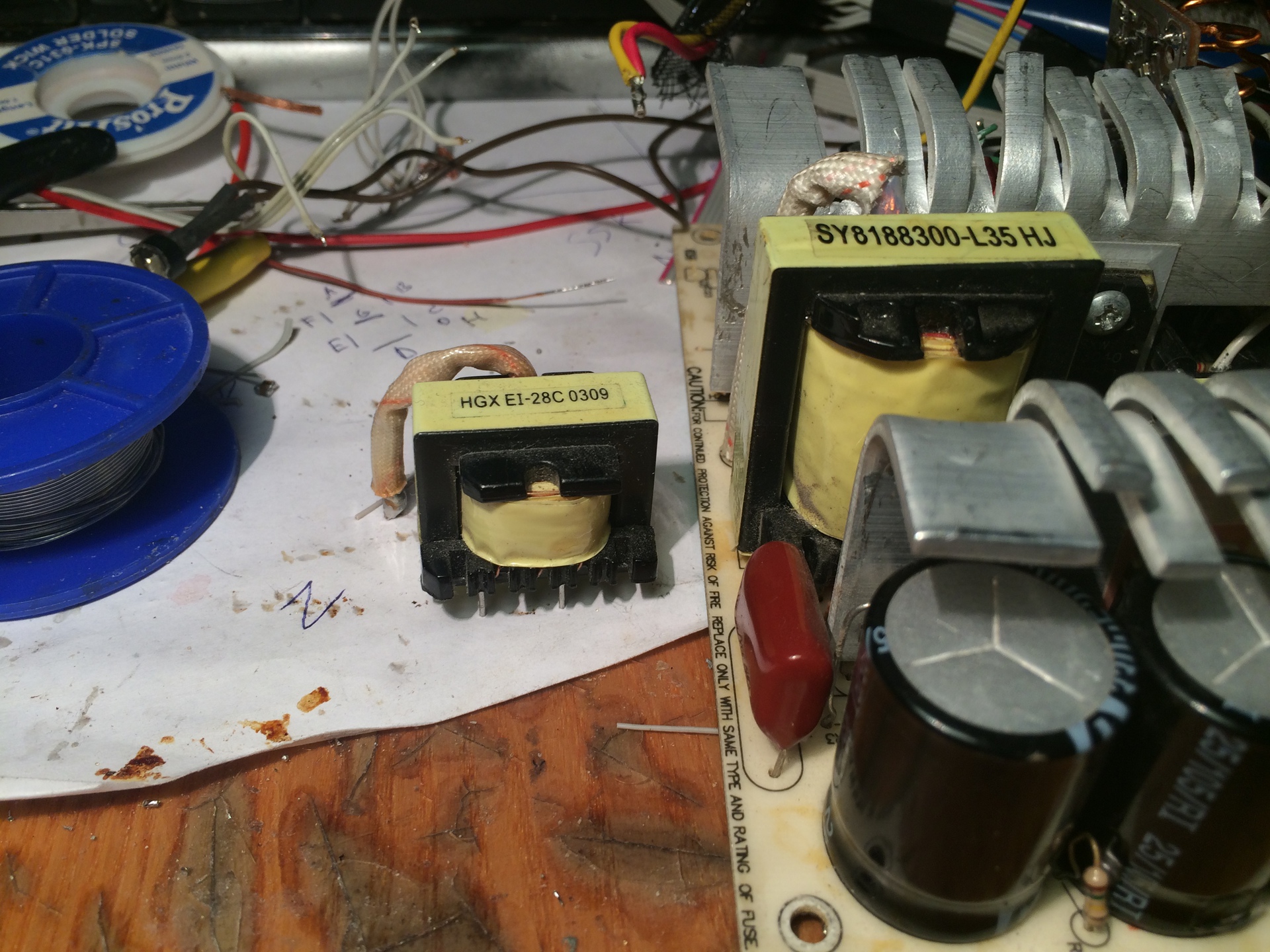
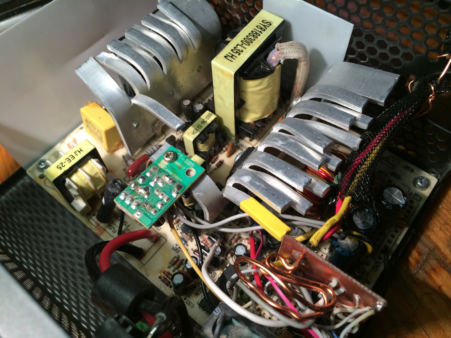
Now we can look at the PSU scheme and understand that there is a lot of excess in it. First of all, I dropped everything related to the control of output voltages (Power good signal conditioning circuit). Neutralized the error amplifiers built into the PWM controller by supplying + 5vref to the inverting inputs and setting the non-inverting to GND. Removed the nominal short circuit protection circuit. I cut out all unnecessary output voltage filters that are not used ... I replaced the output diodes with more powerful ones. Replaced the transformer! Vypayal him from a quality power supply where written 400W really mean 400W. The difference in size between what stood here before it speaks for itself:
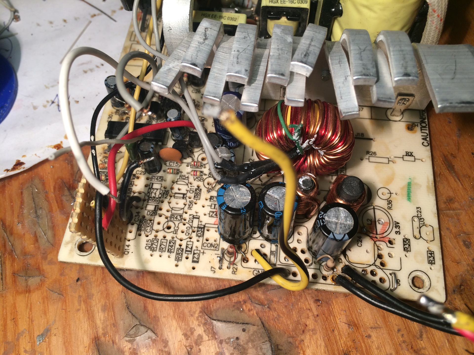
Replaced the chokes in the output filter (from the same 400W power supply) and put the capacitors on 25V:
Next, I developed a scheme that allows you to adjust the stabilization of the output voltage and set the current limit of the output power supply.

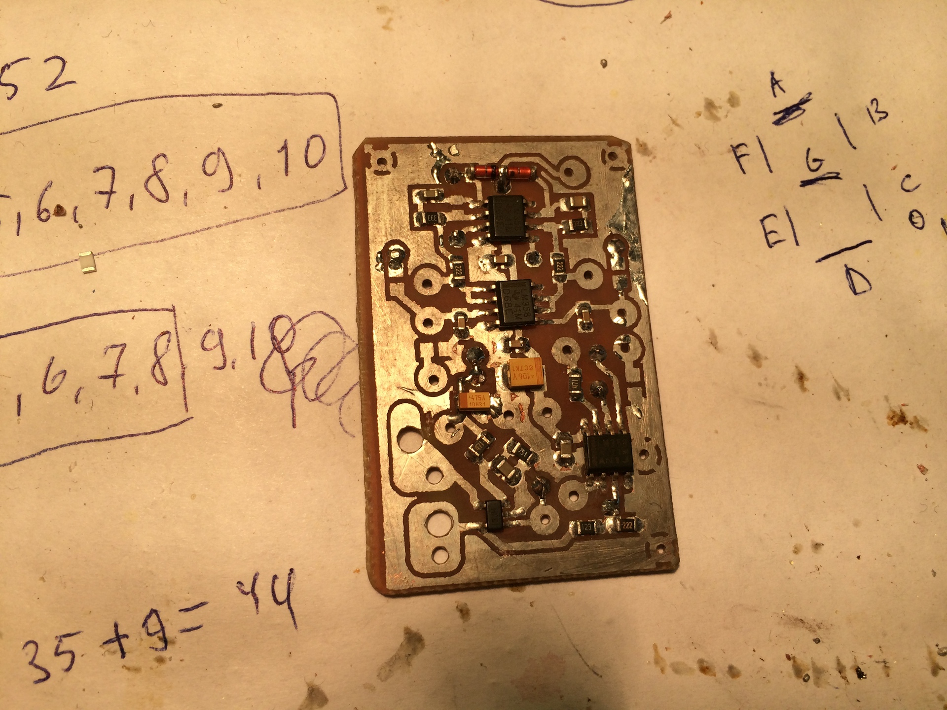
The circuit implements external error amplifiers assembled on LM358 operational amplifiers and several additional functions in the form of a shunt amplifier (INA197) for current measurement, several buffer amplifiers for outputting the value of installed and measured current and voltage to another board where the digital display is assembled. I will tell about it in the next article. Issuing signals to another card as is - not the best solution because The signal source can be quite high resistance, the wire catches noise, making it difficult for the feedback to work steadily. In the first iteration, I ran into this and had to redo everything. In principle, everything is signed on the scheme, I see no point in commenting on it in detail and I think that for those who understood the theory above, everything should be pretty obvious.
I note only that the chains C4R10 and C7R8 are the feedback compensation I mentioned above. Honestly, the fine article embedder under the nickname BSVi really helped in setting it up. bsvi.ru/kompensaciya-obratnoj-svyazi-prakticheskij-podxod This approach really works and after spending a day or two I was able to achieve stable operation of the BP method described in the article. Now, of course, I would have done it in about two hours, probably, but then there was no experience and, through carelessness, I blew quite a few transistors.
Oh yeah, pay attention to the capacity of the C7! 1uF is pretty much. This is done in order to clamp current feedback in speed. This is such a dirty hack to overcome the instability arising at the border of the transition from voltage stabilization to current stabilization. In such cases, they use some more sophisticated techniques, but I did not bother like that. I don’t need super accurate current stabilization, besides, by the time I ran into this disaster, the BP rework project had a great time to get bored!
According to this scheme, a board was made with a laser iron:
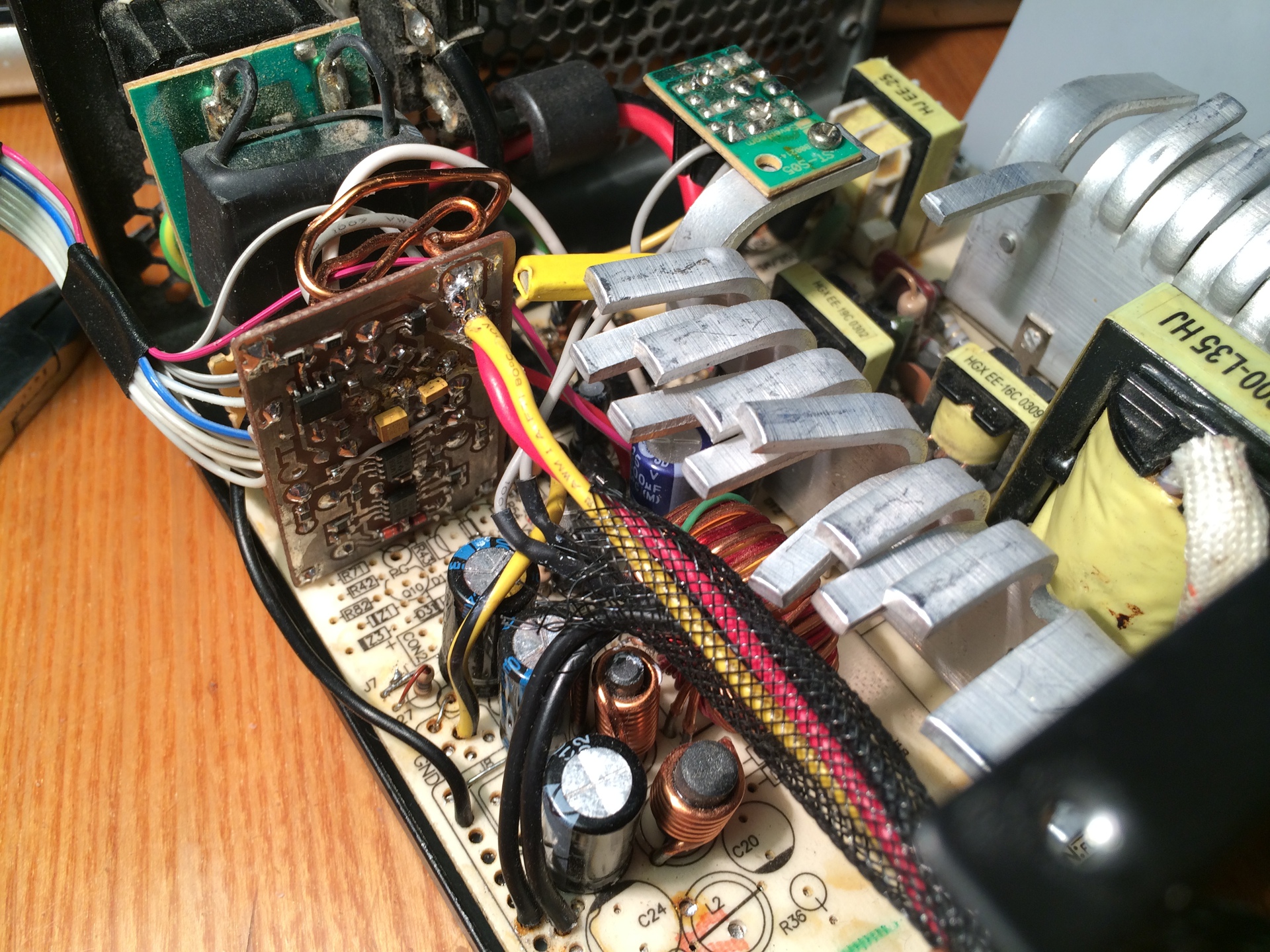
It is built into the power unit like this:
A piece of copper wire 10 centimeters long 10 probably was chosen as a shunt for measuring current.
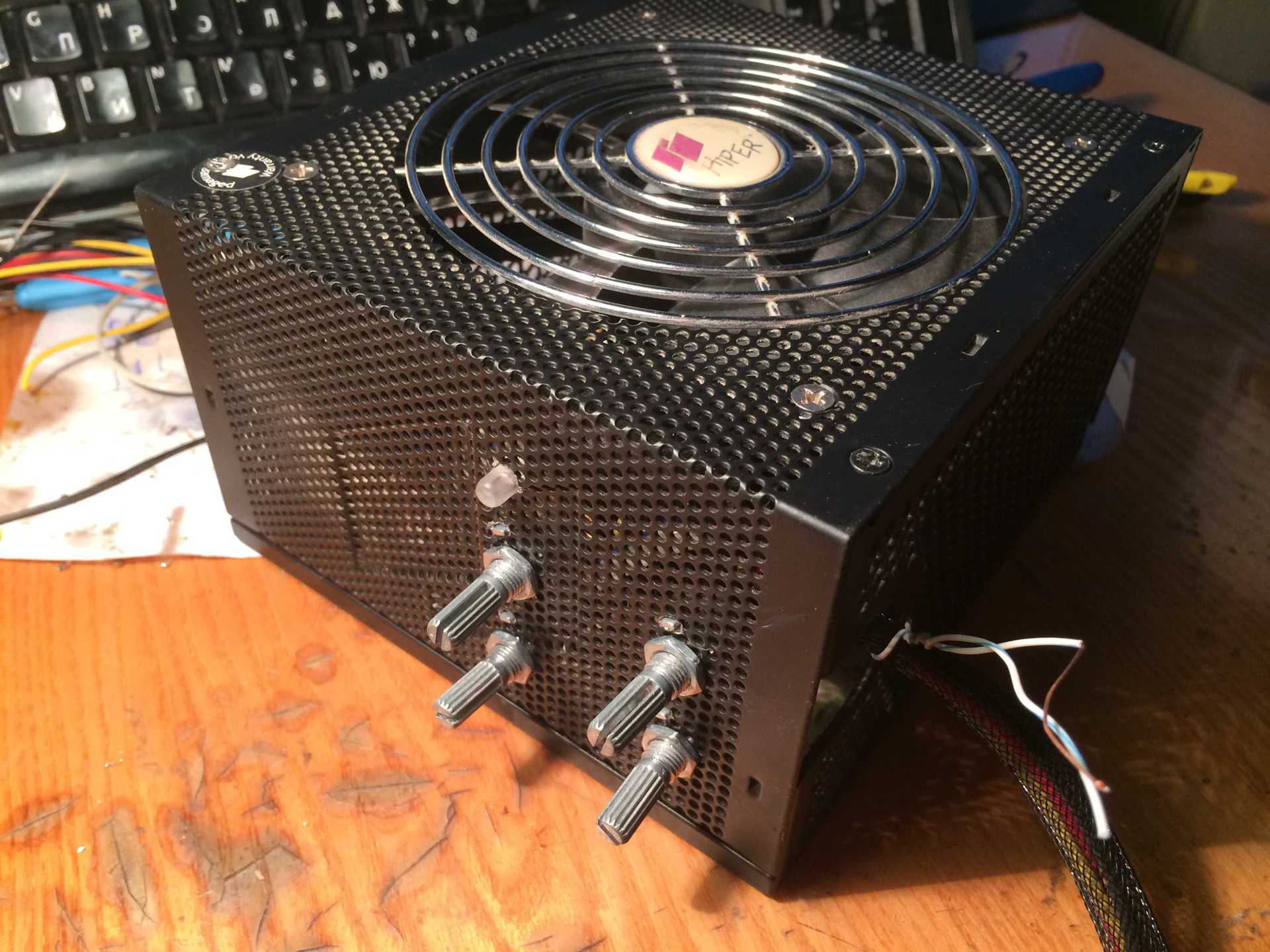
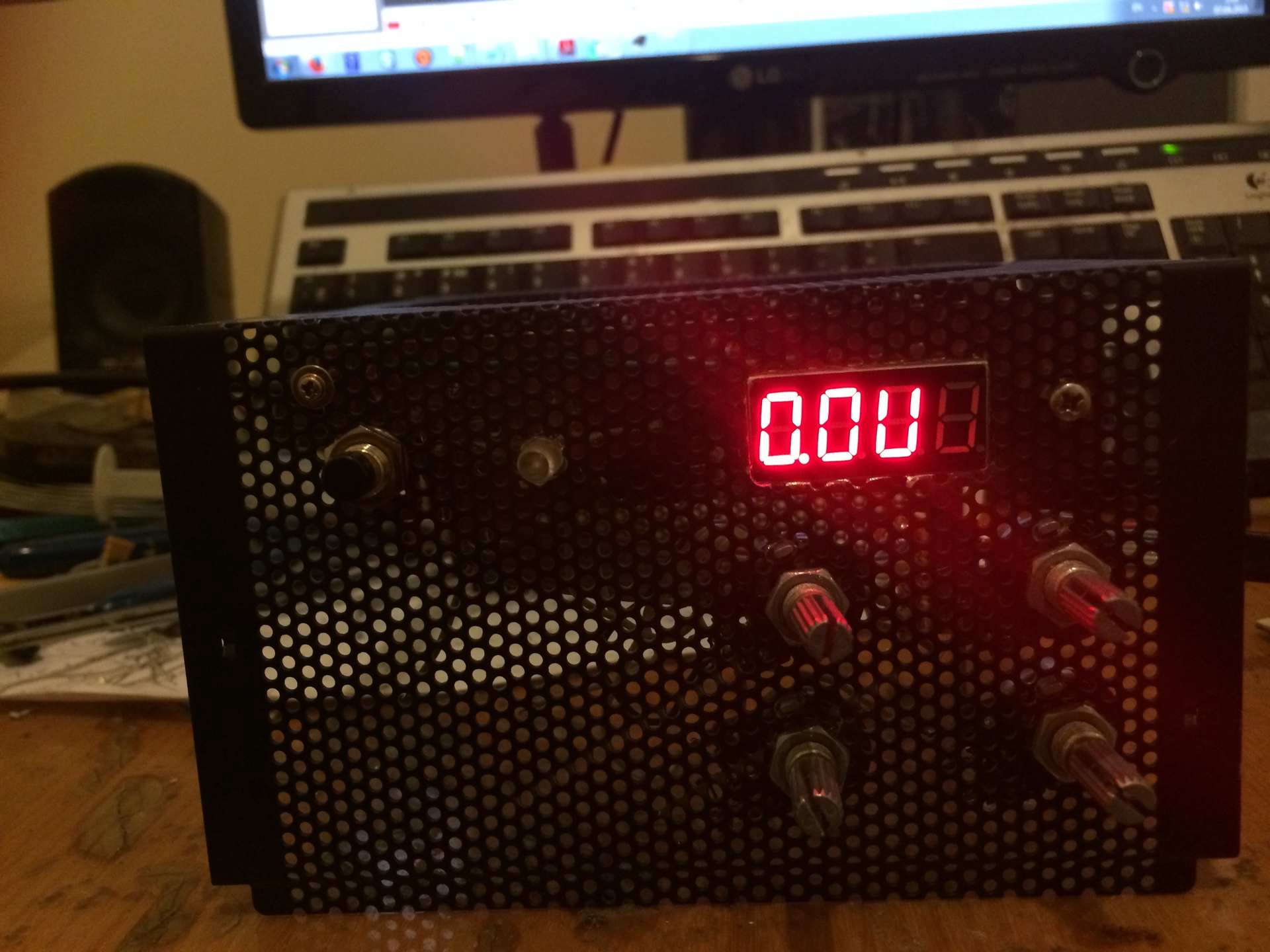
I used the case from a fairly high-quality Hiper PSU. This seems to be the most ventilated hull I've ever seen.
Also there was a question about connecting the fan. BP is regulated from 0 to 24V, which means that the cooler will have to be powered from the duty rooms. The duty is represented by two voltages - stable 5V, which go to the motherboard and not stabilized, service power of about 13.5V, which is used to power the PWM controller itself and to swing the control transformer. I used the usual linear stabilizer to get a stable + 12V and I started them on a small scarf of thermoregulation of the speed of the cooler, evaporated from the same Hiper. The scarf was fastened to the radiator with a screw simply for reasons of ease of connecting the cooler.
Radiators by the way had to bend because they did not fit into the body of the new format. It is better to heat them with a soldering station before bending, otherwise there is a chance to break off half of the teeth. Thermistor regulator secured on the throttle group stabilization because This is the hottest part.
In this form, the PSU underwent long-term tests, powering a bunch of automotive high-beam bulbs and withstanding loads of current of about 20A at a voltage of 14V. And he proudly charged several car batteries when we turned off the lights in the Crimea.
The future is already in the
meantime. In the meantime, I conceived a bit of a nonstandard system of indication of BP operating modes, which I regretted a little later, but it still works!
So in the next article, you will find ATMega8 programming in C ++ using pattern magic, various patterns and a self-writing library for fixed-point calculations on top of which ADC samples are averaged and converted to voltage / current using a table with linear interpolation. By some miracle, all of this fit into 5 with a penny a kilobyte of flash.
Do not switch the channel should be interesting.
By the way, the book promised at the beginning:
Kulichkov A.V. "Pulsed power supplies for the IBM PC"
radioportal-pro.ru/_ld/0/15_caf3ebe8f7eaeee.djvu
PS I hope the above will be useful. Do not judge strictly, but constructive criticism is welcome.
Added for RO users who can not write comments: email: altersoft_poss_mail.ru
Today I would like to tell you about my experience of converting the most common Chinese ATX PSU into a regulated power supply with current and voltage stabilization (0-20A, 0-24V).
In this article we will take a closer look at the operation of the TL494 PWM controller, feedback and go over the modernization of the power supply circuit and the development of a homemade board of error and current error amplifiers.
Honestly, now I can not even name the model of the experimental PSU. One of the many cheap 300W P4 ready. I hope you don’t need to be reminded that in reality this 300W means no more than 150, and then with the appearance of the smell of roast in the apartment.
I expect that my experience will be useful to someone from a practical point of view, and therefore I will focus on theory. Without it, it will still not be possible to remake the BP. in any case there will be some differences in the scheme and complexity during the adjustment.
ATX power supply circuit
To begin, let's go through the ATX power supply circuit on the TL494 controller (and its numerous clones).
All schemes are very similar to each other. Google gives them out quite a lot and it seems I found it almost corresponding to my copy.
Full size link to the diagram
Structurally, we divide the power supply unit into the following units:
- mains voltage rectifier with filter
- standby power supply (+ 5V standby)
- main power supply (+ 12V, -12V, + 3.3V, + 5V, -5V)
- control circuit of the main voltages, generation PowerGood signal and short-circuit protection
Rectifier with filters is all that is in the upper left corner of the circuit to the diodes D1-D4.
The source of standby power is assembled on the transformer T3 and transistors Q3 Q4. Stabilization is based on feedback through the U1 optocoupler and the TL431 reference voltage source. I will not consider in detail the work of this part. I know that too long articles are not very fun to read. At the end I will give the name of the book, where all the details are discussed in detail.
Please note that in the circuit by mistake, the TL494 PWM controller and the TL431 stand-by power ion source are designated as IC1. In the future, I will mention IC1 meaning precisely the PWM controller.
The main power source is assembled on the transformer T1, high-voltage switches Q1 Q2, control transformer T2 and low-voltage switches Q6 Q7. The whole thing is swinging and controlled by the IC1 PWM chip. Understanding the principle of operation of the controller and the purpose of each element of its strapping is just what is needed for the conscious refinement of the BP instead of blindly repeating other people's recommendations and schemes.
The mechanism of operation is approximately as follows: the PWM controller, alternately opening the low-voltage switches Q6 Q7, creates an EMF in the primary winding of the T2 transformer. See, these keys are powered by low voltage from a standby power source? Find on the diagram R46 and understand what I mean. The PWM controller is also powered by this duty voltage. Just above, I called the transformer T2 a control, but it seems that it has some more correct name. Its main task is the galvanic isolation of the low-voltage and high-voltage parts of the circuit. The secondary windings of this transformer control the high-voltage switches Q1 Q2, alternately opening them. With this trick, low-voltage PWM controller can control high-voltage switches in compliance with safety measures. The high-voltage switches Q1 Q2, in turn, swing the primary winding of the T1 transformer and the main voltages of interest arise on its secondary windings. High-voltage, these keys are called because they commute rectified mains voltage, and it is about 300V! The voltage from the secondary windings T1 is rectified and filtered using LC filters.
Now, I hope, the whole picture you imagine and we can go on.
PWM controller TL494.
Let's see how the PWM controller TL494 works.
It would be better if you download the datasheet www.ti.com/lit/ds/symlink/tl494.pdf , but in principle I will try to extract from it the most important thing with the help of pictures. For a deeper understanding of all the subtleties I advise this document: www.ti.com/lit/an/slva001e/slva001e.pdf
We begin, oddly enough, from the end - with the output part of the chip.
Now all the attention to the output element OR (marked with a red square).
The output of this element at a specific point in time directly controls the state of one or both keys Q1 Q2.
The control option is set via pin 13 (Output control).
Important thing number 1: if the output element OR log 1 - output keys are closed (turned off). This is true for both modes.
Important thing number 2: if the output element OR log 0 - one of the keys (or both at once) is open (enabled).
The following picture emerges: on the rising front, the previously opened transistor closes (at this moment both of them are guaranteed to be closed), the trigger changes its state and on the descending front another key is turned on and will remain on until the rising edge comes again and closes it, The moment the trigger is again fliped over and the next descending front will open another transistor. In single ended mode, the keys always work synchronously and the trigger is not used.
The time when the output is in the log. 1 (and both keys are locked) is called Dead time.
The ratio of the pulse duration (log. 0, the transistor is open) to the period of their repetition is called the duty cycle (PWM duty cycle). For example, if the ratio is 100%, then the output element OR is always 0 and the transistor (or both) is always open.
Sorry, but I try to explain as much as possible and almost on my fingers, because this can be read in an official dry language and in a datasheet.
Oh yeah, why do we need Dead time? In short: in real life, the top key will pull up (to plus) and the bottom down (to minus). If you open them simultaneously - there will be a short circuit. This is called through current and because of parasitic capacitances, inductances and other features such a mode arises even if you open the keys strictly in turn. To minimize the through current, dead time is needed.
Now let's pay attention to the saw generator (oscillator), which uses pins 5 and 6 of the chip to set the frequency.
A resistor and a capacitor are connected to these pins. This is the very RC generator about which probably many have heard. Now at pin 5 (CT) we saw from 0 to 3.3V. As you can see, this saw is fed to the inverting inputs of the Comparators Dead-time and PWM.
The terms and the work of the output part of the PWM controller are more or less defined, now we will deal with what it saw and why do we need all these comparators and error amplifiers. We realized that the ratio of the pulse duration to the period of their sequence determines the fill factor, and hence the output voltage of the power source because The more energy is pumped into the primary winding of the transformer, the greater the fill factor.
For example, let's look at what needs to be done to set the fill factor to 50%. Do you still remember about the saw? It is fed to the inverting inputs of the PWM and Dead time comparators. It is known that if the voltage on the inverting input is higher than on the non-inverting input - the comparator output will be log.0. Let me remind you that the saw is a signal that rises smoothly from 0 to 3.3v, after which it drops sharply to 0v.
Thus, at the output of the comparator 50% of the time there was a log.0 — half of the saw voltage must be supplied to the non-inverting input (3.3V / 2 = 1.65V). This will give the desired 50% duty cycle.
We noticed that both comparators converge on the very same OR element, which means that as long as one of the comparators issues log.1, the other cannot prevent it. Those. priority is the comparator, which leads to a lower fill factor. And if the dead time comparator voltage is supplied from the outside, then on the PWM comparator, you can send a signal both from the outside (3 pins) and from the built-in error amplifiers (these are ordinary opamps). They are also connected according to the scheme OR, but since we are already dealing with an analog signal - the OR circuit is implemented using diodes. Thus, the control over the fill factor captures that error amplifier, which asks for a smaller fill factor. The state of the other does not matter.
Feedback.
Well, now how to build a power source on all this? Very simple! It is necessary to cover BP with negative feedback. The difference between the desired (specified) and the available voltage is called an error. If at each moment of time we influence the fill factor so as to correct the error and bring it to 0, we obtain stabilization of the output voltage (or current). Feedback is negative as long as the control action responds to an error with the opposite sign. If the feedback is positive - write is gone! In this case, the feedback will increase the error instead of reducing it.
All this work for those very error amplifiers. A reference voltage (standard) is applied to the inverting input of the error amplifier, and a voltage is applied to the non-inverting input power supply. By the way, inside the PWM controller there is a 5V reference voltage source, which is a reference point in all dimensions.
Compensation feedback
I don’t even know how to explain this in a simpler way. With feedback, everything is simple only in an ideal world. In practice, if you change the fill factor - the output voltage does not change immediately, but with some delay.
For example, the error amplifier registered a voltage drop at the output, corrected the fill factor and stopped interfering with the system, but the voltage continues to increase and then the error amplifier is forced to adjust the fill factor again in the other direction. This situation is due to a delayed reaction. So the system can go into oscillation mode. They are fading and not fading. A power supply unit in which persistent oscillations of the feedback signal may occur will not last long and is unstable.
Feedback has a certain bandwidth. Suppose 100kHz band. This means that if the output voltage oscillates with a frequency higher than 100 kHz, the feedback will simply not notice this and nothing will be corrected. Of course, we would like the feedback to respond to changes in any frequency and the output voltage was as stable as possible. Those. the struggle is to ensure that the feedback is as broadband as possible. However, the very delayed reaction will not allow us to make the band infinitely wide. And if the bandwidth of the feedback circuit is wider than the capacity of the BP itself to test the control signals (direct link) - at some frequencies the negative feedback will suddenly become positive and instead of compensating for the error it will further increase,
Now, from delays in seconds, let's move on to frequencies, gains and phase shifts ...
The bandwidth is the maximum frequency at which the gain is greater than 1.
As the frequency increases, the gain decreases. In principle, this is true for any amplifier.
So, in order for our PSU to work stably, one condition must be met: in the entire frequency band, where the total gain of the forward and feedback link is greater than 1 (0 dB), the phase lag should not exceed 310 degrees. 180 degrees makes the inverting input of the error amplifier.
By entering feedback, various filters ensure that this rule is fulfilled. If it is very rough, then the feedback compensation is the adjustment of the bandwidth and the frequency response of the feedback for the reactions of a real power source (for the characteristics of a direct connection).
This topic is not very simple, under it lies a pile of mathematics, research and other works ... I just try to state the essence of the issue in an accessible form. I can recommend to read this article, where, although not so on the fingers, but this question is also presented in an accessible form and references to the literature are given: bsvi.ru/kompensaciya-obratnoj-svyazi-v-impulsnyx-istochnikax-pitaniya-chast- 1
From theory to practice
Now we can look at the PSU scheme and understand that there is a lot of excess in it. First of all, I dropped everything related to the control of output voltages (Power good signal conditioning circuit). Neutralized the error amplifiers built into the PWM controller by supplying + 5vref to the inverting inputs and setting the non-inverting to GND. Removed the nominal short circuit protection circuit. I cut out all unnecessary output voltage filters that are not used ... I replaced the output diodes with more powerful ones. Replaced the transformer! Vypayal him from a quality power supply where written 400W really mean 400W. The difference in size between what stood here before it speaks for itself:
Replaced the chokes in the output filter (from the same 400W power supply) and put the capacitors on 25V:
Next, I developed a scheme that allows you to adjust the stabilization of the output voltage and set the current limit of the output power supply.
The circuit implements external error amplifiers assembled on LM358 operational amplifiers and several additional functions in the form of a shunt amplifier (INA197) for current measurement, several buffer amplifiers for outputting the value of installed and measured current and voltage to another board where the digital display is assembled. I will tell about it in the next article. Issuing signals to another card as is - not the best solution because The signal source can be quite high resistance, the wire catches noise, making it difficult for the feedback to work steadily. In the first iteration, I ran into this and had to redo everything. In principle, everything is signed on the scheme, I see no point in commenting on it in detail and I think that for those who understood the theory above, everything should be pretty obvious.
I note only that the chains C4R10 and C7R8 are the feedback compensation I mentioned above. Honestly, the fine article embedder under the nickname BSVi really helped in setting it up. bsvi.ru/kompensaciya-obratnoj-svyazi-prakticheskij-podxod This approach really works and after spending a day or two I was able to achieve stable operation of the BP method described in the article. Now, of course, I would have done it in about two hours, probably, but then there was no experience and, through carelessness, I blew quite a few transistors.
Oh yeah, pay attention to the capacity of the C7! 1uF is pretty much. This is done in order to clamp current feedback in speed. This is such a dirty hack to overcome the instability arising at the border of the transition from voltage stabilization to current stabilization. In such cases, they use some more sophisticated techniques, but I did not bother like that. I don’t need super accurate current stabilization, besides, by the time I ran into this disaster, the BP rework project had a great time to get bored!
According to this scheme, a board was made with a laser iron:
It is built into the power unit like this:
A piece of copper wire 10 centimeters long 10 probably was chosen as a shunt for measuring current.
I used the case from a fairly high-quality Hiper PSU. This seems to be the most ventilated hull I've ever seen.
Also there was a question about connecting the fan. BP is regulated from 0 to 24V, which means that the cooler will have to be powered from the duty rooms. The duty is represented by two voltages - stable 5V, which go to the motherboard and not stabilized, service power of about 13.5V, which is used to power the PWM controller itself and to swing the control transformer. I used the usual linear stabilizer to get a stable + 12V and I started them on a small scarf of thermoregulation of the speed of the cooler, evaporated from the same Hiper. The scarf was fastened to the radiator with a screw simply for reasons of ease of connecting the cooler.
Radiators by the way had to bend because they did not fit into the body of the new format. It is better to heat them with a soldering station before bending, otherwise there is a chance to break off half of the teeth. Thermistor regulator secured on the throttle group stabilization because This is the hottest part.
In this form, the PSU underwent long-term tests, powering a bunch of automotive high-beam bulbs and withstanding loads of current of about 20A at a voltage of 14V. And he proudly charged several car batteries when we turned off the lights in the Crimea.
The future is already in the
meantime. In the meantime, I conceived a bit of a nonstandard system of indication of BP operating modes, which I regretted a little later, but it still works!
So in the next article, you will find ATMega8 programming in C ++ using pattern magic, various patterns and a self-writing library for fixed-point calculations on top of which ADC samples are averaged and converted to voltage / current using a table with linear interpolation. By some miracle, all of this fit into 5 with a penny a kilobyte of flash.
Do not switch the channel should be interesting.
By the way, the book promised at the beginning:
Kulichkov A.V. "Pulsed power supplies for the IBM PC"
radioportal-pro.ru/_ld/0/15_caf3ebe8f7eaeee.djvu
PS I hope the above will be useful. Do not judge strictly, but constructive criticism is welcome.
Added for RO users who can not write comments: email: altersoft_poss_mail.ru