Trigger metastability and inter-cycle synchronization
- Tutorial
It is an amazing fact, but many students who have successfully completed a course in digital electronics remain unaware of such a thing as metastability (or consider it so insignificant that they forget about it 2 days after the exam). Meanwhile, device malfunctions caused by metastability are extremely difficult to diagnose. If you recognize yourself in such a student, and if you are at least somehow connected with developments based on digital microcircuits, I highly recommend reading this text. It is possible that by spending 10 minutes now you will save many days spent in future debugging.
The classic D-trigger is the basic unit for storing information in modern digital microcircuits. At a high level of abstraction, it is a memory device with data input D, data output Q, and also an input control clock signal (clk - clock in English terminology). All signals here are logical, they can either be in logical 0 (hereinafter “0”) or in logical 1 (hereinafter “1”). The absolute value of voltages in volts does not interest us yet. When a signal edge arrives at the clock input, i.e. transition from "0" to "1", the trigger remembers the current value at the input of data D and transfers it to output Q. In all other situations, the trigger continues to store its old value. Also, other control signals may be present at the trigger, in particular, the aclr asynchronous reset signal, which sets the trigger to “0”,

Any trigger has two time parameters (requirements) that must be met for the correct operation:

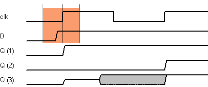
The sum of these two parameters gives us a time window in the vicinity of the clock front during which the input data must be stable. There are similar parameters for other inputs, in particular for an asynchronous reset input (they are called recovery and removal time). Failure to comply with these requirements leads to an undefined trigger state. In the simplest case, it will be either the "old" or the "new" value received at the data input D in the immediate vicinity of the front of the block, but which one is unknown. In many situations, this can be reconciled. In the following picture, the outputs Q (1) and Q (2) are two implementations of the trigger operation when the input time parameters are violated.
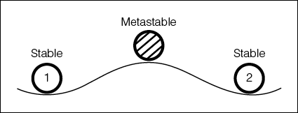
However, sometimes when time parameters are violated, the digital world goes beyond the boundaries and instead of adopting a state that clearly corresponds to “0” or “1”, the trigger output starts to dangle in an intermediate state with a voltage approximately corresponding to half the voltage between “0” and “ 1". A rough analogy from the "mechanical world" is taken out in the header image. In a stable position, the ball is on the left or right. To get into a different state - it needs to be pushed. If you do it strong enough - it will easily pass the top and find itself on the other side (normal trigger switching). If you push too weakly - immediately roll back. If you are a lucky person, then there is a chance that pushing the ball, you make it freeze exactly at the top.
This effect is calledmetastability . In the picture above, this option is designated as Q (3). Ultimately, the trigger will “fall” into one of certain states, but it’s impossible to say exactly when it will happen. The residence time of a trigger in a metastable state is a probabilistic quantity and depends on the technological parameters of the element base, temperature, etc. On the oscilloscope, this picture looks something like this (the input signal violating the trigger time parameters is shown in blue, and the trigger output in pink):

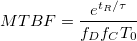
Why is metastability bad? Firstly, this state itself is vague and produces an unknown result in subsequent elements. Moreover, in many cases, the output signal of one trigger is applied immediately to several other elements, which, due to the imperfect technology base, may have slightly different response thresholds. So, the same signal can be interpreted as “1” in one place and as “0” in another. This can lead to a mismatch of the various parts of the device and a general malfunction (i.e. such a situation from which the device itself is unable to exit). Moreover, if the metastable state lasted until the arrival of the next clock signal, then it can enter the next trigger in the chain into the metastable state as well. The probability of this is not high, because the range of input voltages at which the trigger falls into metastability is extremely narrow. However, given the fact that such a situation will occur regularly with a high frequency (modern circuits can operate at frequencies up to 1 GHz, or even higher), this event is quite real. Again, the likelihood of such an event can be estimated taking into account the device parameters, clock frequency and frequency of data changes. The general formula for estimating the time between failures is as follows: clock frequencies and data rate. The general formula for estimating the time between failures is as follows: clock frequencies and data rate. The general formula for estimating the time between failures is as follows:
 where
where
t_R is the time interval of "protection" from metastability. For a rough estimate, we can assume that it is equal to 0 for one trigger, the period of the clock signal minus the delays for presetting and propagation for the second trigger, and plus a period for each subsequent one;
\ tau - technology-dependent parameter, for modern devices, units / tens of picoseconds;
T_0 - time window for getting into metastability. Tens / hundreds of picoseconds;
f_c is the clock frequency. Hundreds of megahertz;
f_D is the frequency of data changes. In the range from 0 to f_c.
For modern equipment, the period when the first trigger in the chain enters the metastable state is measured in micro / milliseconds, the second in hours, and the third in billions-trillions of years.
The effect of metastability can occur in several classic situations:

But first, a few words about where the many clock signals come from. Of course, the easiest and most enjoyable option is when there is only one clock signal. Then working with the project is simple and convenient. Unfortunately, this is only possible for very simple devices. Any more or less complex device usually communicates with several external devices / interfaces, each of which can have its own clock signal. For example, we need to receive data from the ADC, buffer it in external dynamic memory, and then transfer it via Ethernet. In this case, we will have at least 3 clock domains unrelated to each other - the ADC interface, the system bus and DDR-memory, as well as a Ethernet interface interface. This means that we are faced with the task of correctly transmitting data (as well as parameters, control signals, status flags, etc.
For starters, the bad news: it is impossible to completely overcome the effect of metastability, so there is always the possibility that the nearest nuclear power plant will suddenly explode or your plane will suddenly crash. However, a number of simple actions can significantly reduce this probability, roughly equaling the probability that tomorrow the archangel Raphael will sound the sound and announce the Day of Judgment. The general tactic is understandable: we put several triggers in a row (as the formula above shows, for realists two synchronizing triggers are quite enough), after which the data can be used. However, there are a number of technical nuances that depend on the type of data transmitted.
The simplest case is that a pseudostatic scalar (one-bit) signal is transmitted. For example, a mode select signal, etc. - switching extremely rarely. In this case, our only concern is protection against metastability - we put two triggers of the receiving frequency and the thing is in the hat. With an uncertainty of 1 clock (we don’t care), it will be transmitted from source to receiver.

1-step enable signal . The difficulty lies in the fact that if the frequencies do not match, there is a high probability of either completely losing the signal (if the receiving frequency is lower than the original) or stretching it for several clock cycles, which is also not great.

The general approach used in this case is to “lengthen” a signal for several clock cycles, transfer it to a new clock domain in a known manner, and select an edge event there, re-generating a signal with a duration of 1 clock cycle.

A multi-bit bus transmitting a single pseudostatic value (for example, a configuration parameter). It would seem that everything is simple - put a pair of triggers on each bit of the bus - what else is needed? However, we know that after exiting a metastable state, a trigger can take on both old and new values. Moreover, even without entering metastability, simply due to slightly different parameters, the trigger of one of the discharges can catch the new value, and the trigger of the other - the old.
In this case, an incorrect value will be present at the output of the bus for at least 1 clock cycle. It will not be equal to either the old or the new one submitted to the entrance. For some schemes this may not matter, but for some it may be important. Therefore, they try to create a more reliable circuit with a confirmation signal indicating at what point it is safe to click the input data to the output.

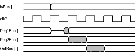
And finally, the most difficult case is the flow of data transmitted from one clock domain to another. If the data is relatively rare (1 data word for 10 or more clock cycles), then you can implement a handshake scheme similar to the previous paragraph. But what if the data goes on each beat (or close to that)? Here, a special hardware unit will come to our aid - a dual-port memory with independent clock signals. Such memory is available both in modern FPGAs and in technological libraries for custom microcircuits. It can be written and read completely independently through two separate ports. The only limitation is the simultaneous access to write and read at the same memory address - it can lead to an undefined result. On the basis of such a memory block, a FIFO module is often created, which allows you to record data from one clock domain on the one hand, and on the other, take it to a different clock domain. At the same time, the FIFO logic ensures that no access to the same memory cell occurs.


In the end, I want to summarize and give some useful tips:
And finally, a few comments on possible technical issues.
Timing diagrams were drawn using the simple free program TimingEditor . Some projects were built at Quartus - solely because of the convenience of its circuit editor. All the same can be (and should be!) Implemented on pure HDL (VHDL / Verilog). If you want a deeper understanding of the physics of metastability, then this topic can be studied in more detail using the keywords metastability and clock domain crossing. For example, Steve Golson’s fairly detailed study, “Synchronization and Metastability,” and Ran Ginosar’s shorter document, “Metastability and Synchronizers,” as well as many others, are available online.
Remember what a trigger is
The classic D-trigger is the basic unit for storing information in modern digital microcircuits. At a high level of abstraction, it is a memory device with data input D, data output Q, and also an input control clock signal (clk - clock in English terminology). All signals here are logical, they can either be in logical 0 (hereinafter “0”) or in logical 1 (hereinafter “1”). The absolute value of voltages in volts does not interest us yet. When a signal edge arrives at the clock input, i.e. transition from "0" to "1", the trigger remembers the current value at the input of data D and transfers it to output Q. In all other situations, the trigger continues to store its old value. Also, other control signals may be present at the trigger, in particular, the aclr asynchronous reset signal, which sets the trigger to “0”,
Any trigger has two time parameters (requirements) that must be met for the correct operation:
- Ts - setup time - preset time. The time during which the signal at input D must remain stable before the arrival of the edge of the clock signal;
- Th - hold time - hold time. The time during which the signal at input D must remain stable after the arrival of the edge of the clock signal;
The sum of these two parameters gives us a time window in the vicinity of the clock front during which the input data must be stable. There are similar parameters for other inputs, in particular for an asynchronous reset input (they are called recovery and removal time). Failure to comply with these requirements leads to an undefined trigger state. In the simplest case, it will be either the "old" or the "new" value received at the data input D in the immediate vicinity of the front of the block, but which one is unknown. In many situations, this can be reconciled. In the following picture, the outputs Q (1) and Q (2) are two implementations of the trigger operation when the input time parameters are violated.
Coin hovering in the air
However, sometimes when time parameters are violated, the digital world goes beyond the boundaries and instead of adopting a state that clearly corresponds to “0” or “1”, the trigger output starts to dangle in an intermediate state with a voltage approximately corresponding to half the voltage between “0” and “ 1". A rough analogy from the "mechanical world" is taken out in the header image. In a stable position, the ball is on the left or right. To get into a different state - it needs to be pushed. If you do it strong enough - it will easily pass the top and find itself on the other side (normal trigger switching). If you push too weakly - immediately roll back. If you are a lucky person, then there is a chance that pushing the ball, you make it freeze exactly at the top.
This effect is calledmetastability . In the picture above, this option is designated as Q (3). Ultimately, the trigger will “fall” into one of certain states, but it’s impossible to say exactly when it will happen. The residence time of a trigger in a metastable state is a probabilistic quantity and depends on the technological parameters of the element base, temperature, etc. On the oscilloscope, this picture looks something like this (the input signal violating the trigger time parameters is shown in blue, and the trigger output in pink):
Why is metastability bad? Firstly, this state itself is vague and produces an unknown result in subsequent elements. Moreover, in many cases, the output signal of one trigger is applied immediately to several other elements, which, due to the imperfect technology base, may have slightly different response thresholds. So, the same signal can be interpreted as “1” in one place and as “0” in another. This can lead to a mismatch of the various parts of the device and a general malfunction (i.e. such a situation from which the device itself is unable to exit). Moreover, if the metastable state lasted until the arrival of the next clock signal, then it can enter the next trigger in the chain into the metastable state as well. The probability of this is not high, because the range of input voltages at which the trigger falls into metastability is extremely narrow. However, given the fact that such a situation will occur regularly with a high frequency (modern circuits can operate at frequencies up to 1 GHz, or even higher), this event is quite real. Again, the likelihood of such an event can be estimated taking into account the device parameters, clock frequency and frequency of data changes. The general formula for estimating the time between failures is as follows: clock frequencies and data rate. The general formula for estimating the time between failures is as follows: clock frequencies and data rate. The general formula for estimating the time between failures is as follows:
where t_R is the time interval of "protection" from metastability. For a rough estimate, we can assume that it is equal to 0 for one trigger, the period of the clock signal minus the delays for presetting and propagation for the second trigger, and plus a period for each subsequent one;
\ tau - technology-dependent parameter, for modern devices, units / tens of picoseconds;
T_0 - time window for getting into metastability. Tens / hundreds of picoseconds;
f_c is the clock frequency. Hundreds of megahertz;
f_D is the frequency of data changes. In the range from 0 to f_c.
For modern equipment, the period when the first trigger in the chain enters the metastable state is measured in micro / milliseconds, the second in hours, and the third in billions-trillions of years.
The effect of metastability can occur in several classic situations:
- Explicit violation of the parameters Ts and Th of the trigger. Usually occurs when the device is trying to get it to work at a frequency at which it cannot physically work due to the too long signal propagation paths. This situation is controlled by a temporary analyzer and should not occur during normal operation (when fulfilling temporary requirements).
- Violation of time parameters for asynchronous reset inputs. Surprisingly, despite the fact that the reset is asynchronous , it must be synchronized with the clock signal of the trigger that resets, i.e. its time parameters are declared relative to the front of the clock pulse. This is often forgotten, giving a dump from nowhere. Again, if the reset signal is generated using the same clock signal as the clock signal of the reset trigger, then the time analyzer will figure it out on its own.
- Signals supplied synchronously (at the same frequency with a known delay) from other devices - here the simplest time analysis (i.e., declaring only the clock frequency) does not work and you need to explicitly set the time characteristics of your input / output signals. This is a separate difficult (but completely solvable) task of temporary analysis.
- And finally, the worst case is that the signals are transmitted asynchronously, maybe at a completely different clock frequency (and with unknown phase shifts) relative to the receiving triggers. Their source can be both external equipment (at least a button on the board or a serial port) and blocks of the same microcircuit operating at a different clock frequency. It is about this situation that further discussion will go.
But first, a few words about where the many clock signals come from. Of course, the easiest and most enjoyable option is when there is only one clock signal. Then working with the project is simple and convenient. Unfortunately, this is only possible for very simple devices. Any more or less complex device usually communicates with several external devices / interfaces, each of which can have its own clock signal. For example, we need to receive data from the ADC, buffer it in external dynamic memory, and then transfer it via Ethernet. In this case, we will have at least 3 clock domains unrelated to each other - the ADC interface, the system bus and DDR-memory, as well as a Ethernet interface interface. This means that we are faced with the task of correctly transmitting data (as well as parameters, control signals, status flags, etc.
How to fight
For starters, the bad news: it is impossible to completely overcome the effect of metastability, so there is always the possibility that the nearest nuclear power plant will suddenly explode or your plane will suddenly crash. However, a number of simple actions can significantly reduce this probability, roughly equaling the probability that tomorrow the archangel Raphael will sound the sound and announce the Day of Judgment. The general tactic is understandable: we put several triggers in a row (as the formula above shows, for realists two synchronizing triggers are quite enough), after which the data can be used. However, there are a number of technical nuances that depend on the type of data transmitted.
The simplest case is that a pseudostatic scalar (one-bit) signal is transmitted. For example, a mode select signal, etc. - switching extremely rarely. In this case, our only concern is protection against metastability - we put two triggers of the receiving frequency and the thing is in the hat. With an uncertainty of 1 clock (we don’t care), it will be transmitted from source to receiver.
1-step enable signal . The difficulty lies in the fact that if the frequencies do not match, there is a high probability of either completely losing the signal (if the receiving frequency is lower than the original) or stretching it for several clock cycles, which is also not great.
The general approach used in this case is to “lengthen” a signal for several clock cycles, transfer it to a new clock domain in a known manner, and select an edge event there, re-generating a signal with a duration of 1 clock cycle.
A multi-bit bus transmitting a single pseudostatic value (for example, a configuration parameter). It would seem that everything is simple - put a pair of triggers on each bit of the bus - what else is needed? However, we know that after exiting a metastable state, a trigger can take on both old and new values. Moreover, even without entering metastability, simply due to slightly different parameters, the trigger of one of the discharges can catch the new value, and the trigger of the other - the old.
In this case, an incorrect value will be present at the output of the bus for at least 1 clock cycle. It will not be equal to either the old or the new one submitted to the entrance. For some schemes this may not matter, but for some it may be important. Therefore, they try to create a more reliable circuit with a confirmation signal indicating at what point it is safe to click the input data to the output.
And finally, the most difficult case is the flow of data transmitted from one clock domain to another. If the data is relatively rare (1 data word for 10 or more clock cycles), then you can implement a handshake scheme similar to the previous paragraph. But what if the data goes on each beat (or close to that)? Here, a special hardware unit will come to our aid - a dual-port memory with independent clock signals. Such memory is available both in modern FPGAs and in technological libraries for custom microcircuits. It can be written and read completely independently through two separate ports. The only limitation is the simultaneous access to write and read at the same memory address - it can lead to an undefined result. On the basis of such a memory block, a FIFO module is often created, which allows you to record data from one clock domain on the one hand, and on the other, take it to a different clock domain. At the same time, the FIFO logic ensures that no access to the same memory cell occurs.
Conclusion
In the end, I want to summarize and give some useful tips:
- The fewer clock signals, the easier it is to work with your project
- The base synchronizer is two (or more) triggers that stand behind each other
- Between all asynchronous clock domains, a data transfer mechanism should be thought out. It is best to draw the clock structure of the project at the stage of system design
- All external signals that are asynchronous to your device, including asynchronous reset signals, must be synchronized.
- Inside one module, it is better to use only one lock
- If there is more than one shred inside the module, then for each internal signal it is necessary to clearly understand what shred it forms and how then it is used. More reliable code directly in the signal name
- Be especially careful at the top level of the project: it is here that very often an erroneous connection of a signal from one clock domain to another occurs without resynchronization
- Clock signals generated by internal frequency multiplication modules (PLL / DCM / MMCM, etc.) are usually synchronous, they are examined by a temporary analyzer, and data resynchronization is most often not required for them. Although it does not hurt.
- Modern design tools try to independently detect situations of data transfer between clock domains. For example, Design Assistant for Altera (built into Quartus), ALINT for Aldec. It is worth listening to warnings and tips.
And finally, a few comments on possible technical issues.
Timing diagrams were drawn using the simple free program TimingEditor . Some projects were built at Quartus - solely because of the convenience of its circuit editor. All the same can be (and should be!) Implemented on pure HDL (VHDL / Verilog). If you want a deeper understanding of the physics of metastability, then this topic can be studied in more detail using the keywords metastability and clock domain crossing. For example, Steve Golson’s fairly detailed study, “Synchronization and Metastability,” and Ran Ginosar’s shorter document, “Metastability and Synchronizers,” as well as many others, are available online.
Only registered users can participate in the survey. Please come in.
Opinion poll
- 44.2% I don’t do electronics, I just went to read 198
- 30.2% Engaged in electronics, I knew about metastability 135
- 25.5% Engaged in electronics, learned a lot 114