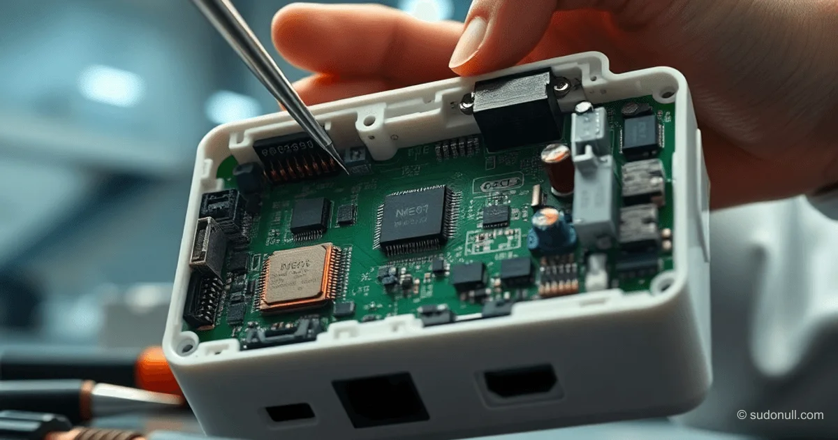
Inside the OnePlus 100W SuperVOOC GaN Charger: A Detailed Teardown
The OnePlus 100W SuperVOOC GaN charger (model VCBAOBCH) delivers 100W via the SuperVOOC protocol, with compatibility for UFCS and QC3.0. Dimensions: 54.82 × 54.33 × 31.44 mm, weight 112 g. Input: 100–130 V / 2.5 A (80W max) or 200–240 V / 2.5 A (100W max). Output: 5 V / 2 A or 5–11 V / 9.1 A. The housing is made of flame-retardant polycarbonate with a matte finish, featuring a USB-A port and a Chinese plug.
Included: charger block + USB-A to USB-C cable (99 cm, red insulation). Testing with the LAB POWER-Z KM003C confirms support for UFCS, QC3.0, SVOOC, VOOC, and DCP protocols. When charging a OnePlus Ace 5 Extreme Edition, it reaches 75.89W.
Teardown and PCBA Topology
PCBA: 50.74 × 50.02 × 24.45 mm. The primary and secondary circuits are isolated with a barrier, potted with compound, with the transformer and USB socket under plastic covers. The bottom is a plastic cover with a heat sink. Key components are glued to the cover for cooling.
Primary Circuit (Input Filter and Rectifier):
- Fuse: Bate Electronics 3.15 A / 250 V.
- NTC thermistors: Jiuyin 8S2R5M for soft-start and inrush current reduction.
- X2 capacitor: CARLI 0.22 μF for differential noise.
- Common-mode filter with inductance in heat shrink.
- Rectifier bridge: DiYi UG8KB100A (8 A, 1000 V, D3K package).
- Electrolytic capacitors: Dongjia 400 V / 33 μF, AiSHi 400 V / 33 μF and 400 V / 27 μF.
Key Power Components and Controllers
The flyback converter controller Southchip SC1835 manages the primary circuit. Power GaN element Navitas NV6134C: eMode GaN FET with driver, 700 V, Rds(on) 260 mΩ, frequency up to 2 MHz, QFN 6×8 mm package.
In the secondary circuit:
- Synchronous rectifier Southchip SC1836 (SOT23-6): CCM/DCM/QR modes, up to 400 kHz, output from 0 V, no additional power winding, adaptive turn-on detection, compliant with CoC V5 / DoE VL.
- NMOS PW028N06ESL (Pingwei): 60 V, Rds(on) 2.3 mΩ, DFN5×6.
- Solid-state capacitors: Emerald 16 V / 820 μF (×2).
Protocols and Output:
- Protocol chip: Southchip SC1834.
- VBUS transistor: 055N03L2 (DFN3×3).
Y-capacitors: HEC Electronics and Haohua Electronics for inter-circuit isolation. Transformer, chip power capacitor Xinzhongyuan 100 V / 10 μF.
List of Key Components
| Component | Model | Manufacturer | Specifications |
|-----------|--------|---------------|----------------|
| PWM Controller | SC1835 | Southchip | Flyback |
| GaN FET+Driver | NV6134C | Navitas | 700 V, 260 mΩ, 2 MHz |
| Sync. Rectifier | SC1836 | Southchip | 400 kHz, CCM/DCM/QR |
| Protocols | SC1834 | Southchip | SuperVOOC/UFC/QC |
| Rectifier Bridge | UG8KB100A | DiYi | 8 A, 1000 V |
| Fuse | - | Bate | 3.15 A / 250 V |
| Input Capacitors | - | AiSHi/Dongjia | 400 V, 27–33 μF |
| Output Capacitors | - | Emerald | 16 V / 820 μF |
Key Takeaways
- Navitas NV6134C GaN implementation enables compact size and high frequency (2 MHz) at 100W.
- Southchip trio (SC1835/1836/1834) optimizes efficiency and protocols without external windings.
- NTC soft-start minimizes inrush current, X/Y capacitors ensure EMI compliance.
- Synchronous rectifier SC1836 with QR mode meets CoC V5 / DoE VL standards.
- Overall design: compact PCBA with potting and heat sink for reliability.
The circuitry combines high-voltage filtering, GaN conversion, and digital protocol control, delivering 100W in a minimal footprint compared to Si-based solutions (e.g., Apple 96W).
— Editorial Team










No comments yet.