DDR SDRAM - design features and signal integrity
Designing electronic devices using fast DDR SDRAM memory modules requires special attention to the problem of signal integrity. The article describes the modern modeling tool for solving such problems.
Today, almost all modern electronics are equipped with memory modules. Servers, computers, smartphones, game consoles, GPS-navigators and most other devices are designed based on processors and FPGAs. Such devices require high-speed, high-bandwidth or double data rate (DDR) memory. With each new generation of DDR SDRAM (synchronous dynamic memory with random access and twice the data transfer rate), the data exchange rate, capacity, memory consumption is reduced.
When designing printed circuit boards for devices with DDR memory, a number of difficulties may arise, one of which is the problem of signal integrity. This article discusses how to ensure the integrity of signals in devices using DDR memory.
Noise and jitter of digital data signal
When receiving / transmitting a memory bus clock signal from the controller to the microcircuit, various interferences can occur due to the jitter of transmitters and receivers, losses in transmission lines, noise and pickup. All this leads to the appearance of jitter and distortion of the digital interface signal.
Any unwanted energy added to the ideal signal can be considered as noise. It can be caused by pickups from neighboring lines, a poorly designed transmission channel, inconsistent impedance, and other factors that lead to a blurring of the pulse front. In the absence of noise, the actual signal is identical to the ideal one.
Any deviation from the ideal waveform affects its integrity. Time variations (jitter) and amplitude / voltage variations (noise) also affect system performance. If the integrity of the signals is not ensured, the DDR system will use incorrect information, which will significantly increase the bit error rate (BER). In the end, the system will work incorrectly and inefficiently.
Consider a specific example. If the engineer connects the transmitter to an inconsistent receiver located at some distance from it, the waveform will be similar to the one shown in Figure 1a: here you can clearly see the ringing at 0.86 V and spurious boost at 1.75 In case of a signal of 1.2 V. All this can lead to a malfunction of the DDR4 logic and, if the circuit board is designed with this topology, then with 100% probability errors will occur in the data stream, which in turn can lead to incorrect system operation .
Theoretically, problems with “ringing” and outliers can be solved by reducing the length of the transmission line, but, unfortunately, this rarely works in practice. The most effective way is to match the receiver / transmitter by impedance, as a result of which the noise level is reduced, and the waveform becomes much better (see Fig. 1b).
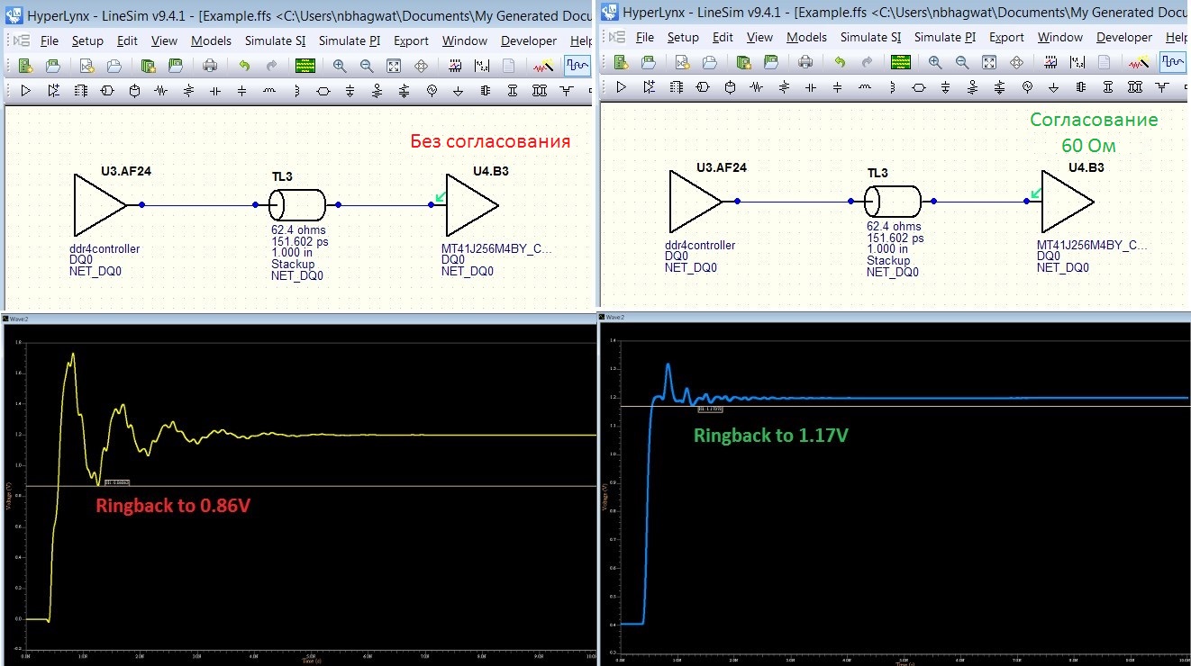
Fig. 1. Topology that has problems with signal quality: a) before approval b) after coordination
This raises the question of which nominal of approval to use and how to calculate it, because even a small change in nominal can significantly affect system performance. The only way to solve this problem is to simulate, in particular, with the help of interactive helpers, the matching settings used in HyperLynx.
Timing problems in DDRx
Since parallel buses operating at gigahertz frequencies, such as DDR3 / 4, are increasingly used in the design of printed circuit boards, signal integrity problems are particularly acute. DDR3 SDRAM, for example, is significantly different in terms of speed and frequency indicators from DDR2: the maximum clock frequency of DDR2 is 800 MHz, and the maximum frequency of DDR3 is 1600 MHz. Due to the reduction in the supply voltage of the cells, the creators of the new type of RAM managed to reduce its power consumption by as much as 15%, which, given the impressive performance of DDR2, can be called a real breakthrough. DDR3 uses the “Fly-by” topology of the command / address / control bus with intra module (ODT) matching. At the same time, DDR3 poses new problems of signal integrity, in particular, related to ODT circuits,
Despite the fact that there are controllers that perform automatic read / write calibration, optimizing the time intervals, the developer needs to ensure the correct timing. The time boundaries in the DDR3 interfaces are so small that an empirical approach to optimization is no longer enough, and in order to guarantee the interface operation at high speeds, a detailed analysis of the circuit is necessary.
Such complex temporal relationships are difficult to analyze without the help of additional tools. In order to identify and eliminate possible problems in general or to calculate complex time relationships, engineers must conduct an analysis of cause-effect relationships, which is a complex and time-consuming task.
Such problems in the design often lead to delays in the planning of projects and, as a result, significantly increase the time to market for the finished product. Advanced, powerful modeling tools can help engineers quickly find errors and correct them by optimizing signals to an acceptable BER level.
Integrity Analysis of DDR SDRAM Systems
The JEDEC Semiconductor Engineering Standardization Committee has approved a list of requirements that must be met when developing high-quality products. It is very important that DDR SDRAM meets these requirements to ensure proper operation and to prevent problems with signal integrity. However, carrying out all the necessary measurements and calculations is often fraught with many difficulties.
Sometimes these calculations can be avoided altogether by strictly following the assembly instructions provided by the supplier of the controller. But what if such recommendations cannot be implemented due to various constraints in specific projects? What to do if it takes a very long time to make sure that the project complies with all the recommendations and requirements? In such situations it is necessary to use the tools to quickly check the project before launching it into production.
With the help of HyperLynx DDR (see Figure 2), you can simulate the entire DDR channel in one iteration. To do this, you only need to bind the appropriate device models that are available on manufacturers' websites. After that, the simulation setup time will take only ten minutes, which will allow further modeling without delays.
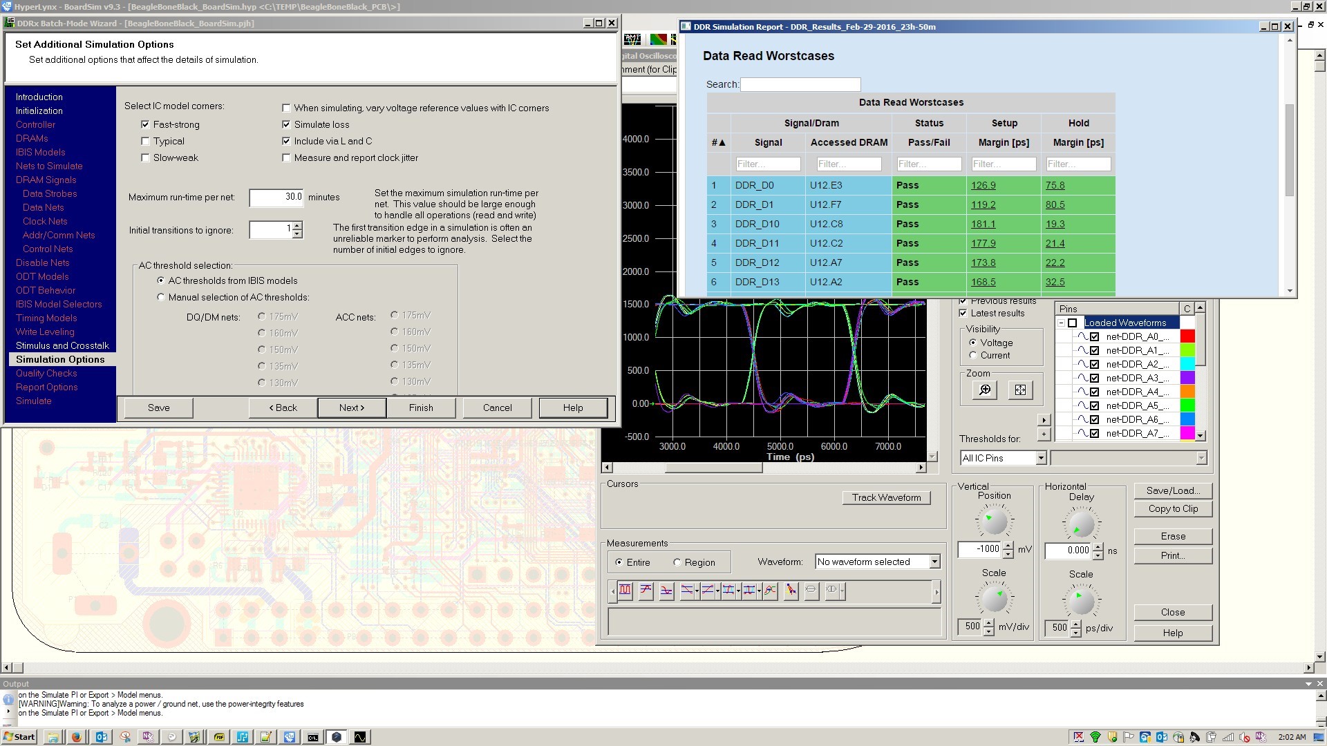
Fig. 2. Modeling with HyperLynx DDR Interactive Assistant
The setup process is intuitively simple, since all the parameters needed to set up the simulation are requested by the assistant interactively. The user simply enters relevant information, such as selecting IBIS models for controllers and memory devices, transfer rates for read / write cycles, ODT, etc. All created configurations can be saved for future use, which will reduce setup time in future projects. Simulations can be performed before or after tracing, helping to determine PCB stack requirements.
Analysis of simulation results
Simulation includes signal integrity analysis and synchronization of the entire DDR bus. Upon completion of the simulation process, a report is created that includes data about passing (not passing) checks, in accordance with the configuration information and data that was entered in the interactive assistant. The results can be filtered and properly organized for a careful study of timing and signal integrity problems in read / write data cycles, in address and command buses or differential circuits. All report results are tied to the relevant simulation data for quick access to the graphical waveform viewer.
The batch mode simulation data created by the DDRx wizard can be saved to disk, allowing you to use a HyperLynx oscilloscope to simultaneously simulate multiple circuits and examine in detail the problems of signal integrity in offline mode.
Conclusion
DDR SDRAM opens up new possibilities in the development of electronic devices. As is the case with other high-speed interfaces, the use of DDR memory has several features. The problem of signal integrity must be carefully studied in order to avoid unnecessary and costly iterations in the manufacture of products. Simulation is a great way to solve this problem, allowing you to take into account effects at the board level, such as changes in impedance and time delays, providing comprehensive control over the memory interface. Powerful analysis tools will help ensure project compliance with JEDEC recommendations and be confident that the final product will work with high performance and reliability.
HyperLynx DDR can be used together by many CAD design PCBs, including PADS and Xpedition.
This article was published in the magazine MODERN ELECTRONICS №7, 2018 (www.soel.ru)