PCB design for small batch production
There are a lot of articles on Habr on setup and maintenance of IP-telephony and related equipment. There are articles on the development of printed circuit boards. There are articles on how to make a printed circuit board yourself using LUT technology. For example, "LUT on vinyl or the home Arduino Mini . " There is a description of various PCB design systems: Cadence , Eagle , DipTrace or a description of individual processes in the development of printed circuit boards, such as transferring information from Altium to AutoCAD .
I want to present an article on how the production of a printed circuit board is set up based on the experience of the company and my own experience in other works. My task is to modernize the existing board to improve the existing qualities and, possibly, to open new horizons that have never been seen before.
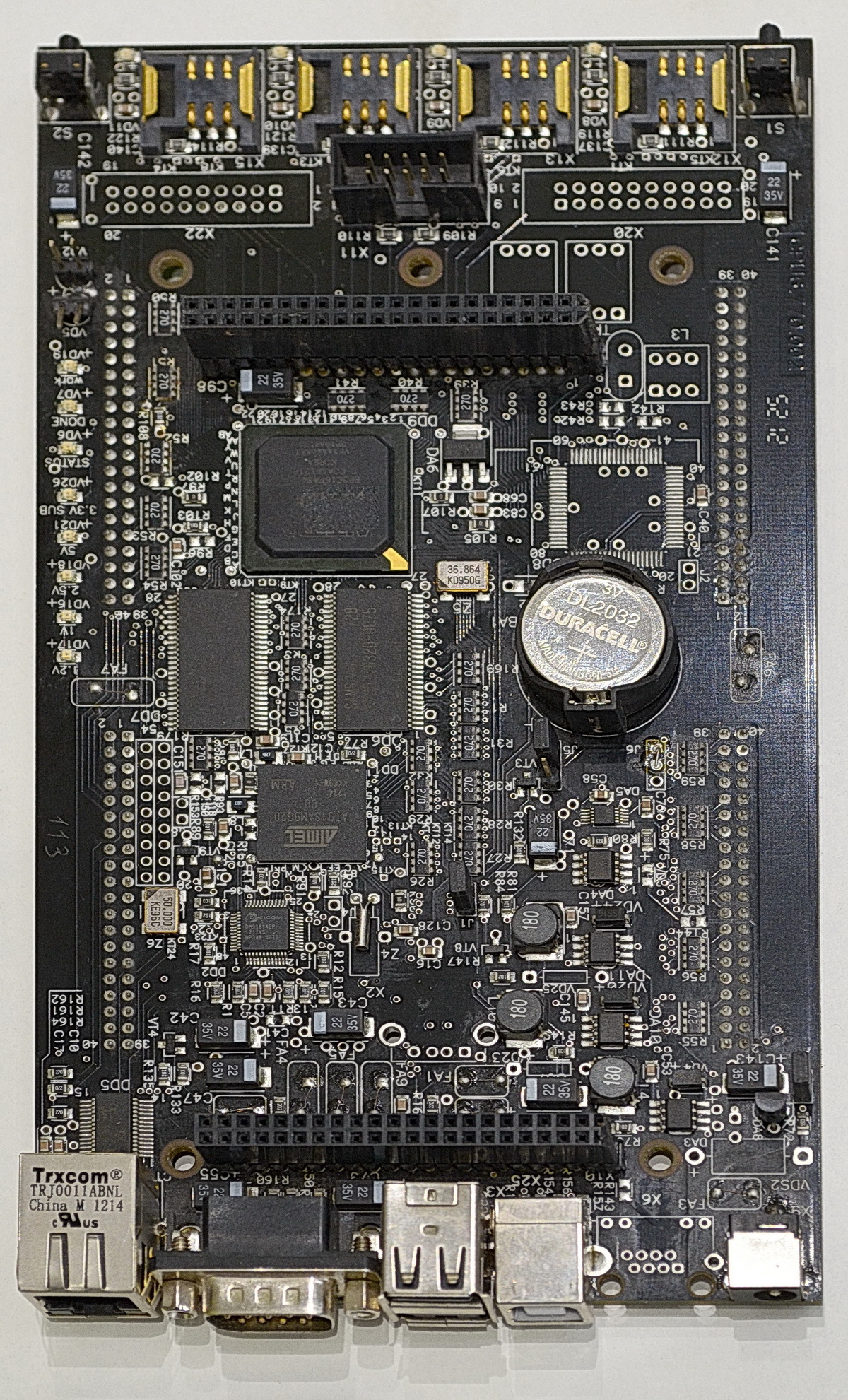
The basis was taken by the CPU board, code-named "G20".
This board subsequently became the main one for many of the company's developments. It will be used with fastened boards in various configurations. Several developers are working on projects for these boards, each with its own add-in and core board.
Once upon a time, even before me, my company developed a wonderful board, thanks to a well-thought-out design, which served as a crust for many devices of the company. The choice was made on the Atmel ARM9 G20 processor, as the FPGA (programmable logic integrated circuit, FPGA in the English literature), Altera uses Cyclone III to communicate with other boards. The connection between the FPGA and the CPU is via a parallel bus, which is compatible with the processor memory bus.
The processor operates at a frequency of 400 MHz, the memory board is equipped with two 512Mbit SRAM chips via a 32 bit bus. The board also has fast ethernet 10/100 and 2 host USB, which can be used both to download the program and to connect to Wi-Fi, a network adapter and other devices. Also in the circuit is a PRI chip that provides an E1 / T1 stream in case of connection to a telephone network.
The board has connectors for connecting auxiliary cards. One board can be connected on top (in the form of a mezzanine), and two on the sides. Two-row connectors with a pitch of 2.54 mm, with soldering in the hole. Their advantage is accessibility, both in price and in store, in the bazaar, in bins. The same applies to mates. Minus - they are large, due to the large step between the contacts they have fewer connecting lines, components with mounting in holes take up space for tracing in all layers of the board, and the connectors for the top board delimit the board into three parts. Mounting in the holes allows you to put the connector both up and down. Although in practice all the boards are placed on top of the main one.
Several types of submodule boards have been developed for this board, which can be structurally called mezzanines. Also, boards can be connected via adapters on the sides of the board.
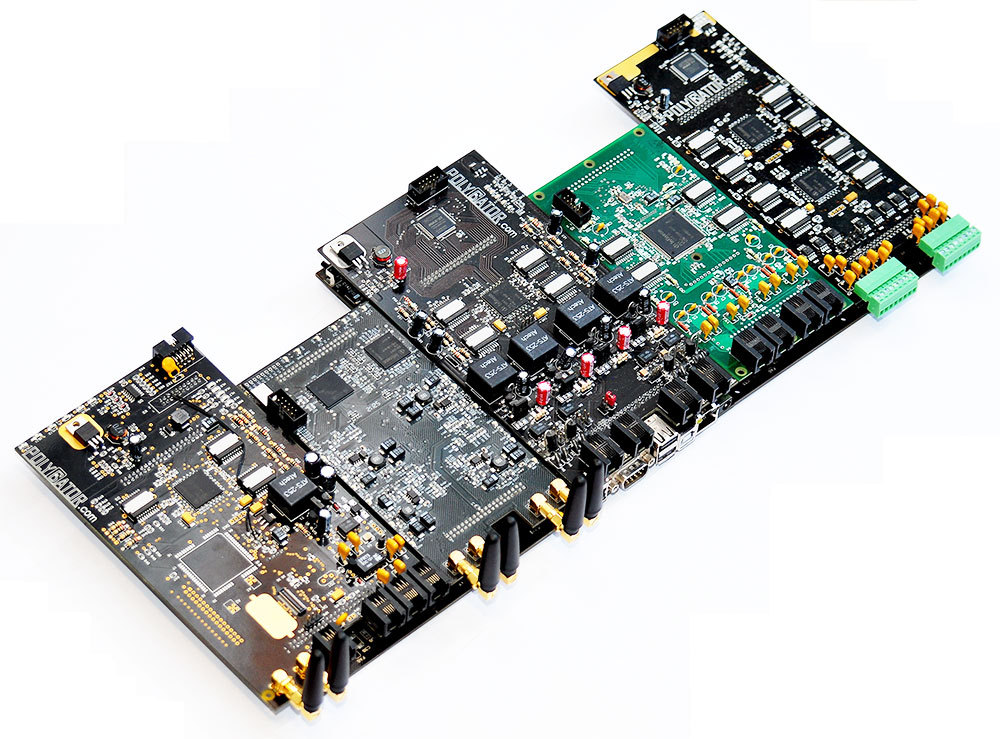
One of these modules is a GSM board for four or eight channels. The removable mezzanine made it possible to develop boards on various GSM modules from different companies and release boards on several ranges (GSM, UMTS, WCDMA). And also install boards for traditional telephony and the creation of PBX with advanced features. There is a version with a SIM bank for 100 SIM cards.
Dividing the functions into several boards made it possible to debug the boards separately from each other and subsequently release improved models of mezzanines.
The board also serves to debug and test individual software modules for future systems. You can connect EvBoard to its contacts and start debugging before making your own board.
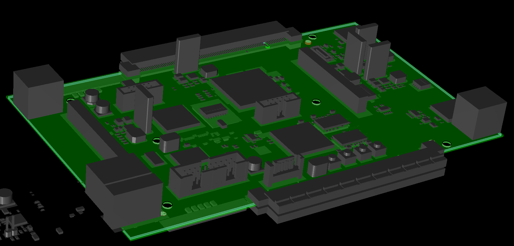
Over time, the capabilities of the main board ceased to be enough and it was decided to develop a new board to replace the existing one. The use of a parallel bus imposed its limitations on the exchange rate and the number of simultaneously loaded boards. This made it possible to draw up requirements for the new board.
The board should have more RAM, a separate bus between the memory and the FPGA, the ability to use fast serial channels to communicate with the boards, and possibly PCIe. At the stage of component selection, additional requirements were added: a built-in programmer for FPGAs, two Ethernet connectors, a USB-hub, HDMI, compatibility with old boards. Part of the interfaces was laid down as separate connectors for connecting devices using a loop.
After analyzing the available processors, the choice fell on the iMX6 from Freescale. Compared to competitors, all the documentation was open for him, he had sane documentation and recommendations available without a long signing of the NDA, a housing suitable for “simple” soldering of BGA, a “normal” memory bus, floating point support, and a number of other advantages. I did not vote for the ARM Cortex-A9 core, floating point support and other buns. Thus, we got a compromise of modern mobile technologies and the capabilities of our production.
The scheme was taken from one of the debugging kits and processed to fit your needs.
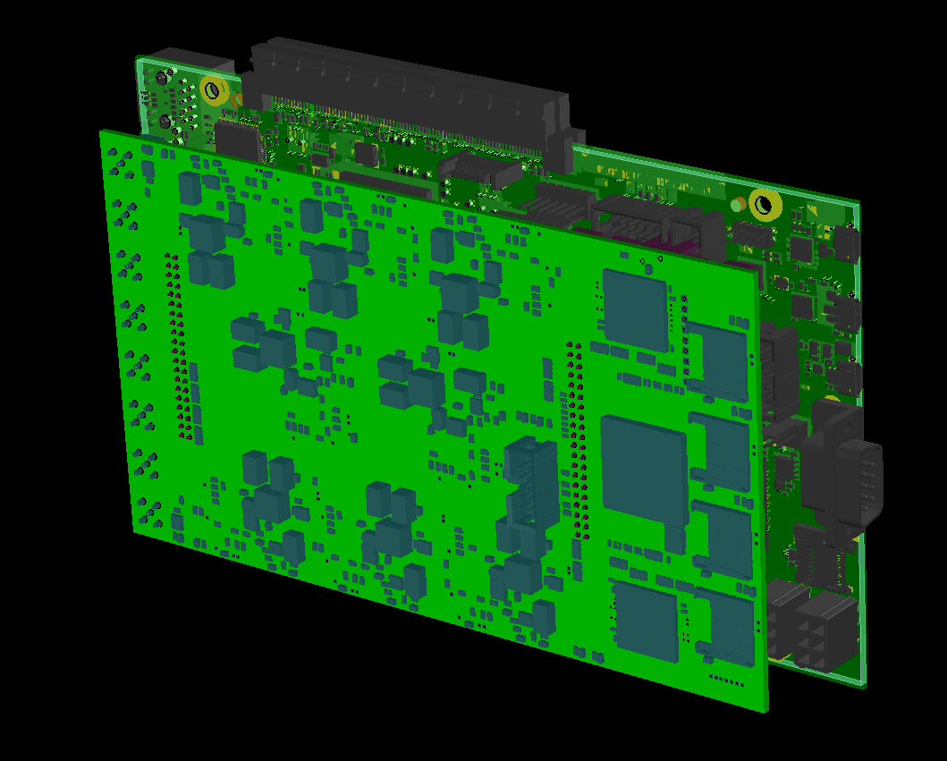
The choice of connectors for side boards is also a compromise between the desire to get a lot of signals parallel and serial and the price of the connectors. The price for a couple of which can exceed 60 cu It was decided to stop at the end PCIe connector. In the future, this will save on a single connector in a pair of boards. In this case, the connector will satisfy both the transmission of fast signals up to 3.125 GHz, which are present in the Cyclone GX.
Since we do not need to use an E-Ink display, we installed FPGAs on a parallel processor bus, additionally connected the PCIe processor bus and a gigabit FPGA bus via a high-speed key. Now our processor can send PCIe either to the FPGA or to one of the side connectors. In addition to PCIe x1, 4 gigabit channels on each side are sent from the processor to the connectors. In the future, it is planned to use them for “quick” connections.
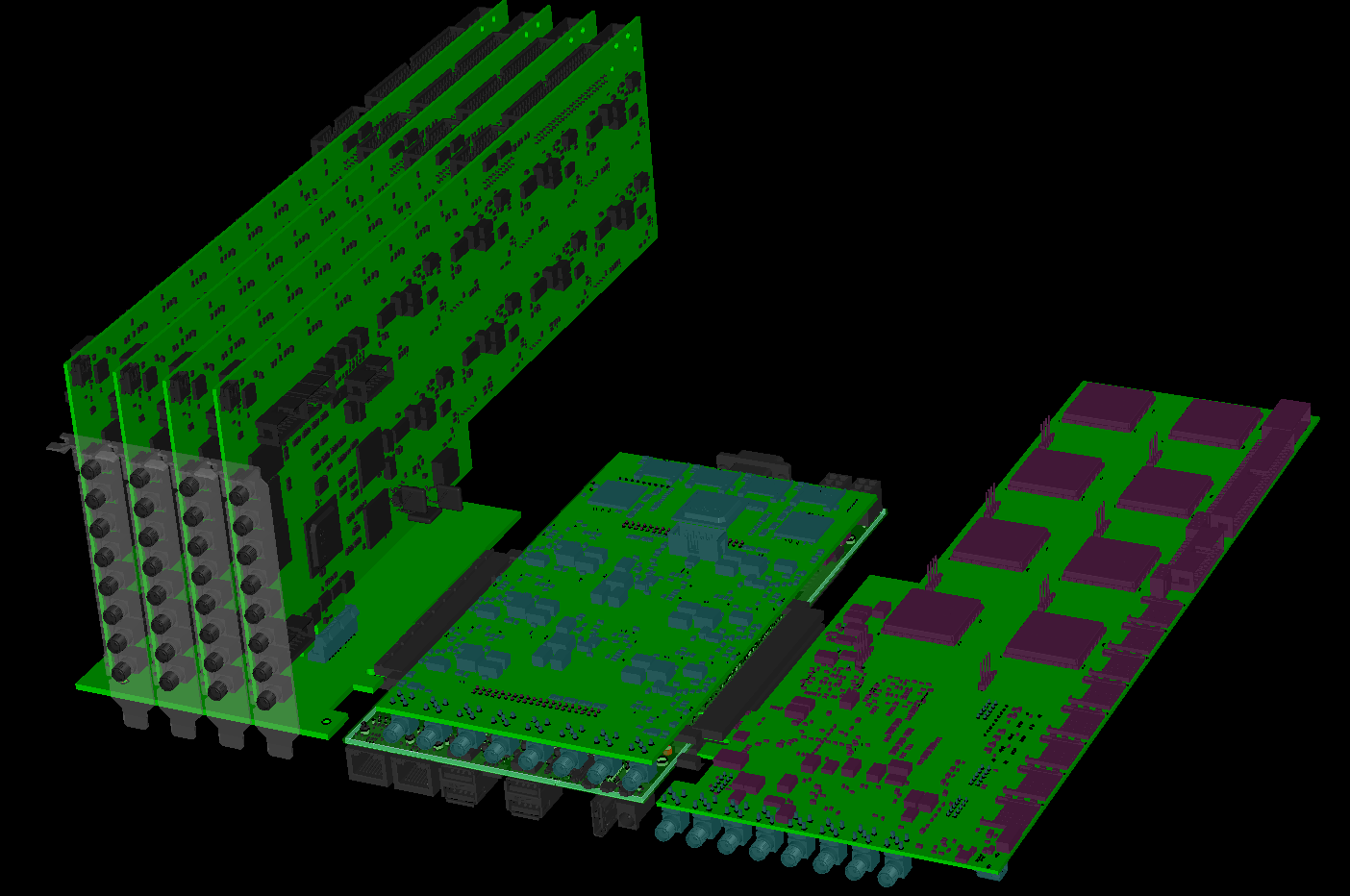
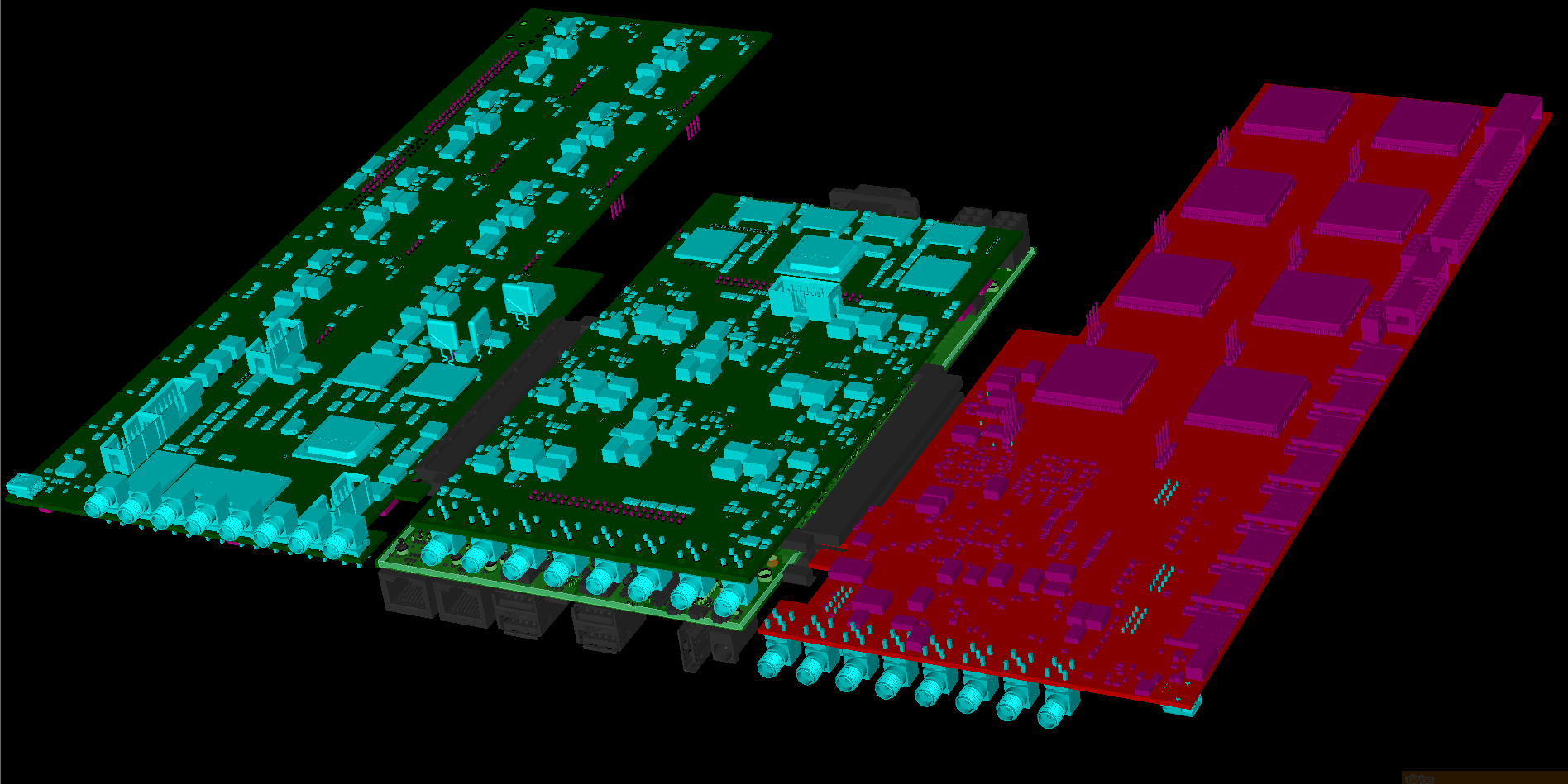
3D modeling inside the design package allows you to "not close" important connectors with other boards.
Next, it was necessary to fit everything into the board sizes we needed, but at the same time leave the possibility of finalizing the board in place for the case “we solder this, we do not solder this”. This approach allows you to make a complex fee from a contract manufacturer, and to solder interfaces for the customer at home. As a result, the customer does not pay for what he uses. These restrictions do not allow you to make everything miniature in the amount of 0201 and place it as close as possible to each other. In addition, sometimes it is necessary to output signals to the outside to be able to solder the jumper. This is a fee for versatility.
We have to look for other ways to minimize the occupied area.
So, for example, capacitors of the same rating and voltage can take up more space in height or in area. Many microcircuits are available in different types of cases and can, with the same functionality, significantly save space.
You can appreciate the differences between SOIC and QFN cases of DC-DC converters. Compared to them, the DDPAK and TO220 cases are simply giants.
Texas Instruments has various types of step-down DC-DC. But modern converters are able to operate at higher frequencies and require a lower value of inductance. If the magnitude of the current is 1-2 A, then you can find inductances and 12 ... 18 μH in acceptable-sized cases. And if you need to provide a current of 5 A or more, then the dimensions of the inductance become too large. The choice of another converter will allow you to go to the inductances 1 ... 2 μH and fit into the overall performance. And not only in area and height, but also in the weight of the components.
When designing a printed circuit board, it is necessary to take into account the influence of the components on each other and try to separate the noise-sensitive circuits from the interference sources. Which, by the way, are pulse DC-DC converters. Therefore, the use of shielded inductances, compensation circuits, and placing secondary power sources away from sensitive circuits can save a bunch of nerves in the future. When it is impossible to spread the elements on the board, you have to trick in various ways by limiting the influence of signals inside the board.
This shows the area of the ground layer near the RF connectors inside the power layer on the PCI gateway PCI card.
Cutout on the inner layer of the earth to reduce the mutual influence of digital and RF noise on the PCI board of the GSM gateway.
It is worth noting that the trace of the printed circuit board for LUT production and for production at the factory is different.
We will also have differences in the requirements for component installation.
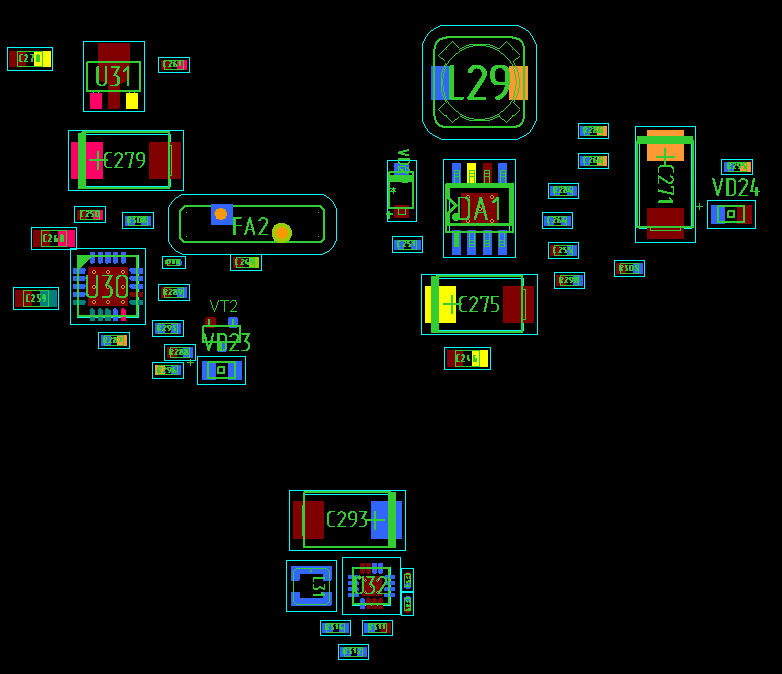
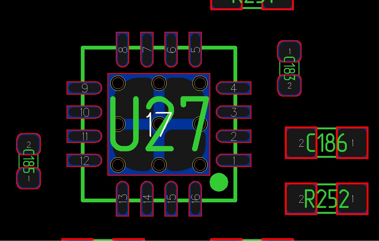
With small batches or a single prototype production, the requirements of the installers can be something like: “I need a board and components, if there is a stencil for mounting SMD components, let's do it.” Often, a component mounting card is sufficient, where sometimes it shows in different colors which components where to install, and sometimes the reference signs are simply indicated. Without specifying the exact coordinates. Below is a piece of such an assembly drawing.
If we are going to make complex boards or simple ones, but of a large volume, then it is worth paying attention to serious contract builders. They have equipment for both installation and testing of assembled circuit boards. They have more requirements. To the quality of printed circuit boards, stencil, components and even tracing.
On printed circuit boards, technological areas around the edges may be required for the board to move along the conveyor. Their sizes depend on the manufacturer and 3 ... 5 mm are enough for our manufacturers. If the components are not mounted on the edge of the board, then technological zones can be omitted. The board will move along the conveyor, leaning on its edges. If the board has uneven contours, then for normal movement along the conveyor it will be necessary to align the contours using technological zones.
Additional equipment for applying solder paste may also be required. For projects with surface mount elements, this is usually a stencil. If you plan to make a large batch of boards or the board will not be single, then it is better to immediately modify the library components “for production”.
By the term “for production” I mean both the assembly production and the production of the boards themselves.
For installers, it is important that all components have the correct footprint.
The seat for the component is usually slightly larger than the soldered element, so that there are gaps in case of inaccuracies in positioning. But they are not worth doing too big. On large sites, the small component can lead away and we get a defective installation. In addition, there may be too much solder paste on a large area, and when melted, the boiling-off flux will lift the component sideways. If the contact pad is large, and the opening for the stencil is reduced, then the solder can spread over the site and will not reach the component leg.
For components with a pitch between leads less than 0.5 mm, it is recommended to open the solder paste in a stencil smaller than the contact area so that the solder paste is not squeezed out by the component installed on it and short circuit and jumpers do not form during reflow.
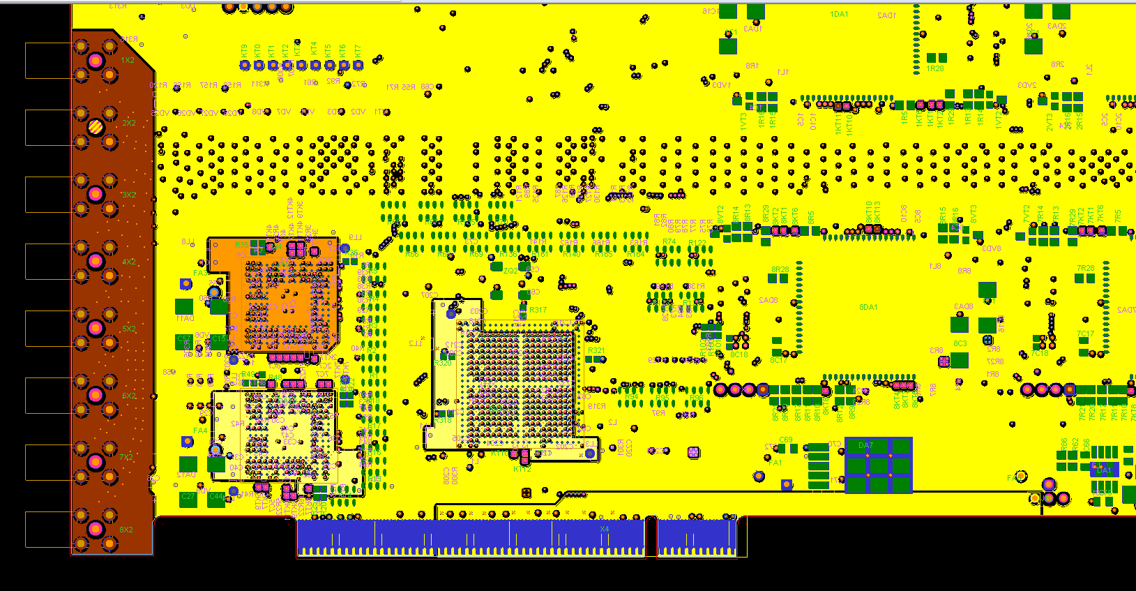
The figure shows the boundary of the opening of the solder mask in red, purple - the contact area, black - opening in the stencil under the solder paste.
Now a lot of components are available in smaller and smaller cases and, despite the increasing efficiency, the developers are faced with the task of removing heat from the chips. So, if the case dimensions are small, then the required amount of heat cannot be dissipated through the cover, and they came up with a “horse ride” - solder the bottom of the chip to the board, and the board already removes heat through the layers of copper.

In practice, I had the opportunity to verify the effectiveness of such a cooling method when thermal protection against overheating was turned on in microcircuits with a non-soldered abdomen, and when the temperature of the microcircuits decreased after soldering, and the boards increased and even the connectors began to heat up, as heat was discharged to the ground layer to which the connector housings were soldered.
So, you need to carefully read the recommendations for the design of seats for such microcircuits, since some of them have no other contact with the ground, except for the "abdomen". And if you do not put solder paste under the contact, then the microcircuit will not be connected to the ground. For microcircuits with a small number of legs, thermal drops under the case are small, and for large microcircuits you need to be careful. Manufacturers indicate in the recommendations which contact pad and which hole in the stencil for solder paste should be made. Sometimes just 60 - 70% of the thermal drop is indicated in the documentation, and sometimes recommendations are given for dividing a large window in the stencil into several small ones, then when applying solder paste it will not be squeezed out of the large holes with a spatula.
In order for the component installation system to be able to correctly install the component, it needs a reference point on the board and the installation coordinates of the components with an angle of rotation. You can read more about this by looking for information on reference marks on printed circuit boards or PCB fiducials. The coordinate file is prepared automatically in the PCB design program.
I get a similar file with tabs at the output.
Header:
$
HEADER $ BOARD_TYPE PCB_DESIGN
UNITS MM
$ END HEADER
Part with components:
$ PART_SECTION_BEGIN $
R303 RC0402FR-0768KL 270.00 120.30 39.10 BOTTOM YES
C580 CC0402-KR-X5R-5BB-104 180.00 38.40
TOP.80N 4040.5040.5040.5040.5040.40
...
C282 CC0402-KR-X5R-7BB - 104 180.00 128.10 26.20 BOTTOM YES
VS2 BZT52C-3V3 90.00 71.40 27.10 BOTTOM YES
the U23 MCIMX6Q4AVT08AC 0.00 106.00 45.90 TOP of NO
$ PART_SECTION_END $
Coordinates with repeernymi signs:
$ FIDUCIAL_SECTION_BEGIN $
BOARD 42.50 8.00 BOTTOM
BOARD 177.00 8.00 BOTTOM
BOARD 183.40 113.50 BOTTOM
BOARD 183.40 113.50 TOP
BOARD 177.00 8.00 TOP
BOARD 42.50 8.00 TOP
U23 94.50 57.40 TOP
U23 117.50 34.40 TOP
U10 22.70 87.00 TOP
U10 38.70 109.00 TOP
U18 52.50 69.50 TOP
U18 81.50 98.50 TOP
$ FIDUCIAL_SECTION_
Small boards require combining small boards into a group blank or panel. Both PCB backing manufacturers and installers have this requirement. For installation, the coordinates of the components for one board, the step of the boards in the workpiece, and the angle of rotation of the board in the workpiece are given.
Board rotation is mainly necessary to reduce the area of the workpiece with a curved circuit board. But rectangular boards can also be rotated in the panel. Once at the assembly plant they demanded to increase the technological indent from 5 to 30 mm for one side of the board, since there it was necessary to put components with a small pitch very close to the edge of the board. When combining the boards into a panel, the problematic edge of the boards was deployed in the middle of the panel and the technological margin remained on all sides 5 mm. This made it possible to place two panels on one large sheet of fiberglass in the production of a printed circuit board. At the same time, the customer of the board did not overpay for board waste.
Panel for the manufacture of gas meter boards.
After installation, the panel boards can be disconnected at the installation site, or easily separated from us. Next comes verification, firmware, setup, packaging and pre-sale preparation.
These are not all the stages of preparing boards and devices for production. You can add minimization of the list of components, checking for manufacturability, developing the case and placing components on the board and other operations, but I tried to describe the actions that I had to do.
PS There is still no photo for the new board, since it has not arrived yet. Based on the scheme of the new board, a board is now being made in the dimensions of the old one and without unnecessary frills in the form of an expensive FPGA display and other things.
I want to present an article on how the production of a printed circuit board is set up based on the experience of the company and my own experience in other works. My task is to modernize the existing board to improve the existing qualities and, possibly, to open new horizons that have never been seen before.
The basis was taken by the CPU board, code-named "G20".
This board subsequently became the main one for many of the company's developments. It will be used with fastened boards in various configurations. Several developers are working on projects for these boards, each with its own add-in and core board.
Once upon a time, even before me, my company developed a wonderful board, thanks to a well-thought-out design, which served as a crust for many devices of the company. The choice was made on the Atmel ARM9 G20 processor, as the FPGA (programmable logic integrated circuit, FPGA in the English literature), Altera uses Cyclone III to communicate with other boards. The connection between the FPGA and the CPU is via a parallel bus, which is compatible with the processor memory bus.
The processor operates at a frequency of 400 MHz, the memory board is equipped with two 512Mbit SRAM chips via a 32 bit bus. The board also has fast ethernet 10/100 and 2 host USB, which can be used both to download the program and to connect to Wi-Fi, a network adapter and other devices. Also in the circuit is a PRI chip that provides an E1 / T1 stream in case of connection to a telephone network.
The board has connectors for connecting auxiliary cards. One board can be connected on top (in the form of a mezzanine), and two on the sides. Two-row connectors with a pitch of 2.54 mm, with soldering in the hole. Their advantage is accessibility, both in price and in store, in the bazaar, in bins. The same applies to mates. Minus - they are large, due to the large step between the contacts they have fewer connecting lines, components with mounting in holes take up space for tracing in all layers of the board, and the connectors for the top board delimit the board into three parts. Mounting in the holes allows you to put the connector both up and down. Although in practice all the boards are placed on top of the main one.
Several types of submodule boards have been developed for this board, which can be structurally called mezzanines. Also, boards can be connected via adapters on the sides of the board.
One of these modules is a GSM board for four or eight channels. The removable mezzanine made it possible to develop boards on various GSM modules from different companies and release boards on several ranges (GSM, UMTS, WCDMA). And also install boards for traditional telephony and the creation of PBX with advanced features. There is a version with a SIM bank for 100 SIM cards.
Dividing the functions into several boards made it possible to debug the boards separately from each other and subsequently release improved models of mezzanines.
The board also serves to debug and test individual software modules for future systems. You can connect EvBoard to its contacts and start debugging before making your own board.
Over time, the capabilities of the main board ceased to be enough and it was decided to develop a new board to replace the existing one. The use of a parallel bus imposed its limitations on the exchange rate and the number of simultaneously loaded boards. This made it possible to draw up requirements for the new board.
The board should have more RAM, a separate bus between the memory and the FPGA, the ability to use fast serial channels to communicate with the boards, and possibly PCIe. At the stage of component selection, additional requirements were added: a built-in programmer for FPGAs, two Ethernet connectors, a USB-hub, HDMI, compatibility with old boards. Part of the interfaces was laid down as separate connectors for connecting devices using a loop.
After analyzing the available processors, the choice fell on the iMX6 from Freescale. Compared to competitors, all the documentation was open for him, he had sane documentation and recommendations available without a long signing of the NDA, a housing suitable for “simple” soldering of BGA, a “normal” memory bus, floating point support, and a number of other advantages. I did not vote for the ARM Cortex-A9 core, floating point support and other buns. Thus, we got a compromise of modern mobile technologies and the capabilities of our production.
The scheme was taken from one of the debugging kits and processed to fit your needs.
The choice of connectors for side boards is also a compromise between the desire to get a lot of signals parallel and serial and the price of the connectors. The price for a couple of which can exceed 60 cu It was decided to stop at the end PCIe connector. In the future, this will save on a single connector in a pair of boards. In this case, the connector will satisfy both the transmission of fast signals up to 3.125 GHz, which are present in the Cyclone GX.
Since we do not need to use an E-Ink display, we installed FPGAs on a parallel processor bus, additionally connected the PCIe processor bus and a gigabit FPGA bus via a high-speed key. Now our processor can send PCIe either to the FPGA or to one of the side connectors. In addition to PCIe x1, 4 gigabit channels on each side are sent from the processor to the connectors. In the future, it is planned to use them for “quick” connections.
3D modeling inside the design package allows you to "not close" important connectors with other boards.
Next, it was necessary to fit everything into the board sizes we needed, but at the same time leave the possibility of finalizing the board in place for the case “we solder this, we do not solder this”. This approach allows you to make a complex fee from a contract manufacturer, and to solder interfaces for the customer at home. As a result, the customer does not pay for what he uses. These restrictions do not allow you to make everything miniature in the amount of 0201 and place it as close as possible to each other. In addition, sometimes it is necessary to output signals to the outside to be able to solder the jumper. This is a fee for versatility.
We have to look for other ways to minimize the occupied area.
So, for example, capacitors of the same rating and voltage can take up more space in height or in area. Many microcircuits are available in different types of cases and can, with the same functionality, significantly save space.
You can appreciate the differences between SOIC and QFN cases of DC-DC converters. Compared to them, the DDPAK and TO220 cases are simply giants.
Texas Instruments has various types of step-down DC-DC. But modern converters are able to operate at higher frequencies and require a lower value of inductance. If the magnitude of the current is 1-2 A, then you can find inductances and 12 ... 18 μH in acceptable-sized cases. And if you need to provide a current of 5 A or more, then the dimensions of the inductance become too large. The choice of another converter will allow you to go to the inductances 1 ... 2 μH and fit into the overall performance. And not only in area and height, but also in the weight of the components.
When designing a printed circuit board, it is necessary to take into account the influence of the components on each other and try to separate the noise-sensitive circuits from the interference sources. Which, by the way, are pulse DC-DC converters. Therefore, the use of shielded inductances, compensation circuits, and placing secondary power sources away from sensitive circuits can save a bunch of nerves in the future. When it is impossible to spread the elements on the board, you have to trick in various ways by limiting the influence of signals inside the board.
This shows the area of the ground layer near the RF connectors inside the power layer on the PCI gateway PCI card.
Cutout on the inner layer of the earth to reduce the mutual influence of digital and RF noise on the PCI board of the GSM gateway.
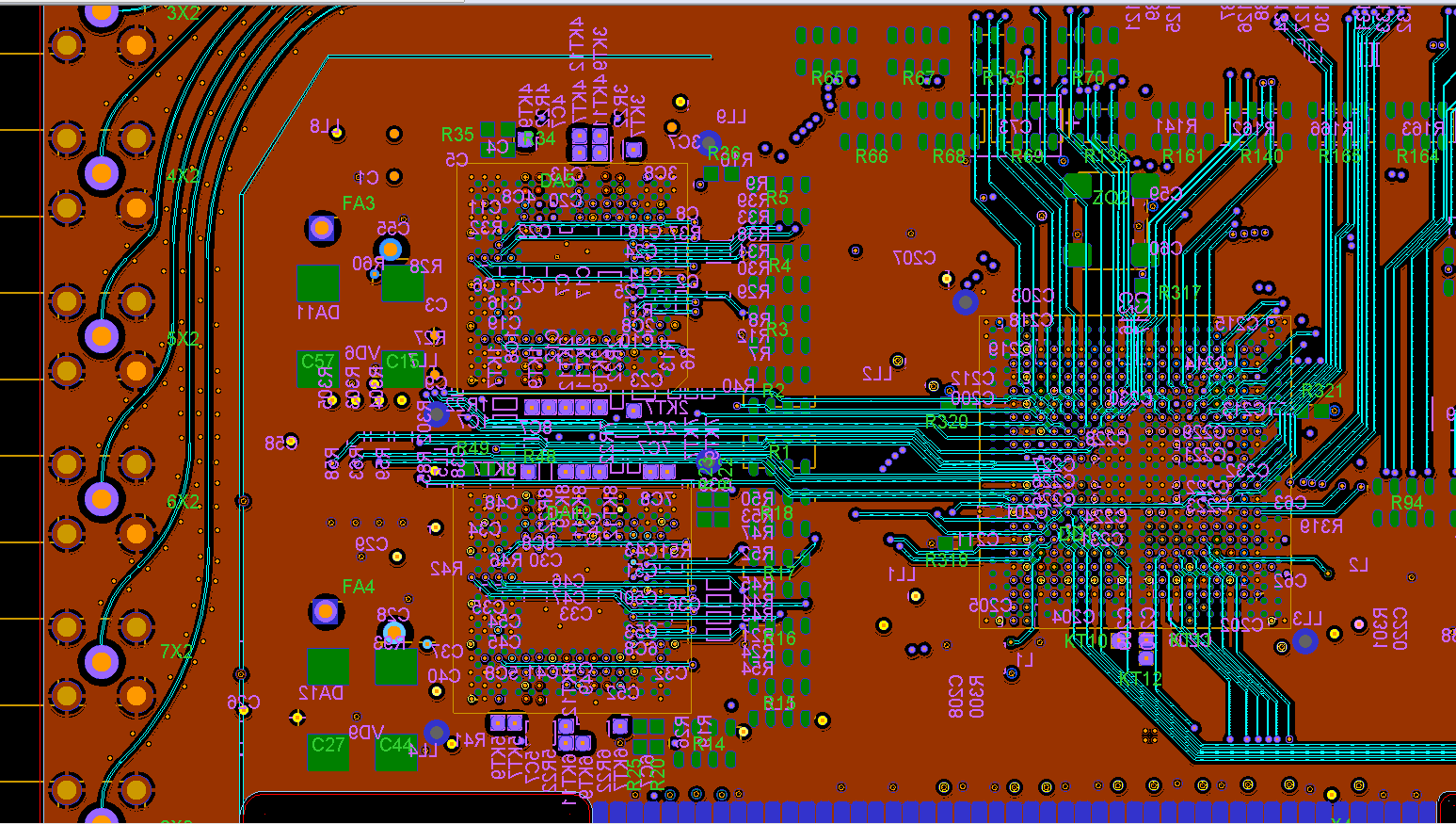
It is worth noting that the trace of the printed circuit board for LUT production and for production at the factory is different.
We will also have differences in the requirements for component installation.
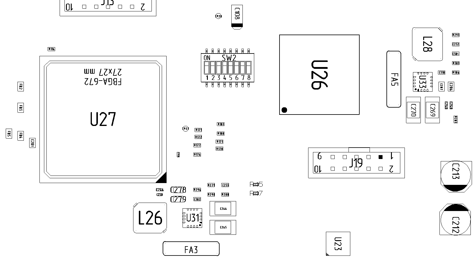
With small batches or a single prototype production, the requirements of the installers can be something like: “I need a board and components, if there is a stencil for mounting SMD components, let's do it.” Often, a component mounting card is sufficient, where sometimes it shows in different colors which components where to install, and sometimes the reference signs are simply indicated. Without specifying the exact coordinates. Below is a piece of such an assembly drawing.
If we are going to make complex boards or simple ones, but of a large volume, then it is worth paying attention to serious contract builders. They have equipment for both installation and testing of assembled circuit boards. They have more requirements. To the quality of printed circuit boards, stencil, components and even tracing.
On printed circuit boards, technological areas around the edges may be required for the board to move along the conveyor. Their sizes depend on the manufacturer and 3 ... 5 mm are enough for our manufacturers. If the components are not mounted on the edge of the board, then technological zones can be omitted. The board will move along the conveyor, leaning on its edges. If the board has uneven contours, then for normal movement along the conveyor it will be necessary to align the contours using technological zones.
Additional equipment for applying solder paste may also be required. For projects with surface mount elements, this is usually a stencil. If you plan to make a large batch of boards or the board will not be single, then it is better to immediately modify the library components “for production”.
By the term “for production” I mean both the assembly production and the production of the boards themselves.
For installers, it is important that all components have the correct footprint.
The seat for the component is usually slightly larger than the soldered element, so that there are gaps in case of inaccuracies in positioning. But they are not worth doing too big. On large sites, the small component can lead away and we get a defective installation. In addition, there may be too much solder paste on a large area, and when melted, the boiling-off flux will lift the component sideways. If the contact pad is large, and the opening for the stencil is reduced, then the solder can spread over the site and will not reach the component leg.
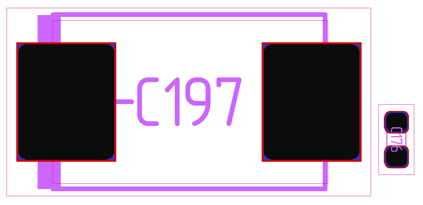
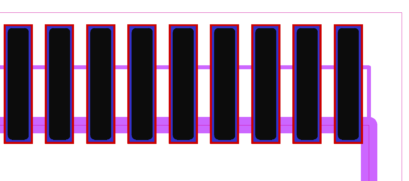
For components with a pitch between leads less than 0.5 mm, it is recommended to open the solder paste in a stencil smaller than the contact area so that the solder paste is not squeezed out by the component installed on it and short circuit and jumpers do not form during reflow.
The figure shows the boundary of the opening of the solder mask in red, purple - the contact area, black - opening in the stencil under the solder paste.
Now a lot of components are available in smaller and smaller cases and, despite the increasing efficiency, the developers are faced with the task of removing heat from the chips. So, if the case dimensions are small, then the required amount of heat cannot be dissipated through the cover, and they came up with a “horse ride” - solder the bottom of the chip to the board, and the board already removes heat through the layers of copper.
In practice, I had the opportunity to verify the effectiveness of such a cooling method when thermal protection against overheating was turned on in microcircuits with a non-soldered abdomen, and when the temperature of the microcircuits decreased after soldering, and the boards increased and even the connectors began to heat up, as heat was discharged to the ground layer to which the connector housings were soldered.
So, you need to carefully read the recommendations for the design of seats for such microcircuits, since some of them have no other contact with the ground, except for the "abdomen". And if you do not put solder paste under the contact, then the microcircuit will not be connected to the ground. For microcircuits with a small number of legs, thermal drops under the case are small, and for large microcircuits you need to be careful. Manufacturers indicate in the recommendations which contact pad and which hole in the stencil for solder paste should be made. Sometimes just 60 - 70% of the thermal drop is indicated in the documentation, and sometimes recommendations are given for dividing a large window in the stencil into several small ones, then when applying solder paste it will not be squeezed out of the large holes with a spatula.
In order for the component installation system to be able to correctly install the component, it needs a reference point on the board and the installation coordinates of the components with an angle of rotation. You can read more about this by looking for information on reference marks on printed circuit boards or PCB fiducials. The coordinate file is prepared automatically in the PCB design program.
I get a similar file with tabs at the output.
Header:
$
HEADER $ BOARD_TYPE PCB_DESIGN
UNITS MM
$ END HEADER
Part with components:
$ PART_SECTION_BEGIN $
R303 RC0402FR-0768KL 270.00 120.30 39.10 BOTTOM YES
C580 CC0402-KR-X5R-5BB-104 180.00 38.40
TOP.80N 4040.5040.5040.5040.5040.40
...
C282 CC0402-KR-X5R-7BB - 104 180.00 128.10 26.20 BOTTOM YES
VS2 BZT52C-3V3 90.00 71.40 27.10 BOTTOM YES
the U23 MCIMX6Q4AVT08AC 0.00 106.00 45.90 TOP of NO
$ PART_SECTION_END $
Coordinates with repeernymi signs:
$ FIDUCIAL_SECTION_BEGIN $
BOARD 42.50 8.00 BOTTOM
BOARD 177.00 8.00 BOTTOM
BOARD 183.40 113.50 BOTTOM
BOARD 183.40 113.50 TOP
BOARD 177.00 8.00 TOP
BOARD 42.50 8.00 TOP
U23 94.50 57.40 TOP
U23 117.50 34.40 TOP
U10 22.70 87.00 TOP
U10 38.70 109.00 TOP
U18 52.50 69.50 TOP
U18 81.50 98.50 TOP
$ FIDUCIAL_SECTION_
Small boards require combining small boards into a group blank or panel. Both PCB backing manufacturers and installers have this requirement. For installation, the coordinates of the components for one board, the step of the boards in the workpiece, and the angle of rotation of the board in the workpiece are given.
Board rotation is mainly necessary to reduce the area of the workpiece with a curved circuit board. But rectangular boards can also be rotated in the panel. Once at the assembly plant they demanded to increase the technological indent from 5 to 30 mm for one side of the board, since there it was necessary to put components with a small pitch very close to the edge of the board. When combining the boards into a panel, the problematic edge of the boards was deployed in the middle of the panel and the technological margin remained on all sides 5 mm. This made it possible to place two panels on one large sheet of fiberglass in the production of a printed circuit board. At the same time, the customer of the board did not overpay for board waste.
Panel for the manufacture of gas meter boards.
After installation, the panel boards can be disconnected at the installation site, or easily separated from us. Next comes verification, firmware, setup, packaging and pre-sale preparation.
These are not all the stages of preparing boards and devices for production. You can add minimization of the list of components, checking for manufacturability, developing the case and placing components on the board and other operations, but I tried to describe the actions that I had to do.
PS There is still no photo for the new board, since it has not arrived yet. Based on the scheme of the new board, a board is now being made in the dimensions of the old one and without unnecessary frills in the form of an expensive FPGA display and other things.