Plis Achronix - development experience
For more than a ten-year period of working with FPGAs, I happened to work with products from four different manufacturers. With such a variety, one involuntarily draws attention to both the general features of the development process and the features inherent in a particular company. And now, a couple of months ago, I suddenly had the unique opportunity to get to know the new FPGA family, produced by a small but ambitious company from California. I am talking about the youngest FPGA manufacturer - the company Akroniks (Achronix) and its FPGA Speedster22i HD1000.
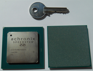
Since its inception (2004), this young company has been able to develop HI-End FPGAs with original architecture and unique features. Moreover, the company was the first among all FPGA manufacturers to enter into a strategic alliance with Intel Corporation and has since been manufacturing its own microchips (the size of which, as can be seen from the figure, has long gone beyond the "micro") at Intel's most advanced technological base in factories located directly to the USA. Now the Speedster series is available in 3D Tri-Gate 22nm technology. The development program of the series provides in the near future the transition to 14nm and 10nm process technology (as they are mastered at Intel plants).
In this review article, I want to briefly describe, on the one hand, those products that are used to work with Speedster FPGAs, and on the other hand, my experience (including emotions) in working with these products using an example of a very simple but really completed project. So …
Iron and development tools
Perhaps the only way to get acquainted with the Speedster22i FPGA at work is to buy (receive as a gift, rent, lease ...) the Speedster22i HD1000 Development Kit debugging kit, which we did. In the process of waiting for delivery, preparatory work was done: a powerful computer with water cooling, 32GB RAM and two monitors was purchased. In order to get development tools, I had to register on the Achronix website (http://www.achronix.com/company/contact-us.html) and get a user account. A user account allows access to the site area containing the necessary software for work, as well as demo and link designs. What is the difference between them? Reference designs come with source code for FPGAs,
Registration confirmation took a couple of days and ended with receiving an email containing a username and password. After that, it became possible to download the necessary tools to get started - Achronix's own shell called ACE and the Synplify synthesizer. But in order for these programs to work, they also need license files. To do this, fill out another form and specify the MAC address of the network card. License files are sent by email. Their connection also did not cause any problems, in addition, this process is described in detail in the documentation. Windows is installed on my computer, but development tools are also available for Red Hat Linux.
The time remaining until the board arrived was devoted to studying the architecture of the FPGA Speedster22i HD1000, mastering the design tools and writing a simple design.
What is interesting about the Speedster22i series? What distinguishes it from products of other companies? FPGA Speedster22i has its own “highlight” - hardware IP-cores focused on high-speed communication tasks. Achronix FPGA cores are still out of competition. Nomenclature of cores: DDR-3 - 6 pcs., PCI Express Gen1 / 2/3 x1, x4, x8 - 2 pcs., Ethernet MAC up to 100G - 2 pcs., Interlaken - 2 pcs. This provides a total throughput of over 400 Gb / s, which, of course, allows us to classify FPGAs of the Speedster22i series as HI-END.
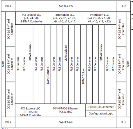
Otherwise, the FPGAs under consideration in their structure are not very different from the products of other manufacturers: they consist of logical clusters (based on 4-input LUTs), block and distributed memory, as well as arithmetic blocks including powerful 56-bit multipliers. All this is available in sufficient quantities to achieve the most complex functionality. Speed characteristics are also impressive: the memory, for example, has a maximum operating frequency of 750 MHz. The main characteristics of the FPGA of the Speedster22i series are given in the table below:
| Parameters | HD680 | HD1000 | HD1500 |
| Logic scope, including hardware controllers (effective LUT cells) | 660,000 | 1045000 | 1725000 |
| Programmable Logic Volume (in LUT) | 400,000 | 700,000 | 1,100,000 |
| Number of BRAM Modules | 600 | 1026 | 1728 |
| Number of LRAM Modules | 4320 | 6156 | 10368 |
| The volume of 80 kilobit BRAM (total Kbit) | 48000 | 82080 | 138240 |
| 640-bit LRAM capacity (total Kbps) | 2765 | 3940 | 6636 |
| Multipliers (28 × 28) | 240 | 756 | 864 |
| The number of lines SerDes 12.75 GB / s (Gigabit / s) | 40 | 64 | 48 |
| The number of lines SerDes 28 gb / s (Gigabit / s) | - | - | 16 |
| Ethernet hardware controllers (MAC layer) 10/40/100 Gigabit / s | 2 | 2 | 4 |
| Interlaken LLC controllers | 1 | 2 | 4 |
| PCI Express LLC Controllers | 1 | 2 | 2 |
| DDR2 / DDR3 controllers | 4 | 6 | 6 |
| PLL Number | 16 | 16 | 16 |
| Number of pins, case FBGA2601 52.5 × 52.5 (12G, 28G, GPIO) | - | 64,0,960 | 48.16.960 |
| Number of pins, case FBGA1936 45 × 45 (12G, 28G, GPIO) | 40,0,684 | 40,0,684 | 20,4,684 |
| Number of pins, case FBGA1520 40 × 40 (12G, 28G, GPIO) | 18,0,684 | - | - |
The minimum required set of development tools includes two programs - the ACE shell and the Synplify synthesizer. The company's own development - the ACE shell includes facilities for placing and wiring, configuring cores, loading and debugging. As a synthesizer, the Synplify program from Synopsys is used. The approach of using a set of separate programs instead of a single integrated environment is typical for small companies. It is less convenient for beginner developers, but for experienced engineers it gives greater flexibility and better quality of execution of each stage. If deeper integration is required, all the required software tools can be combined, for example, through the HDL-designer shell from MentorGraphics.
It is advisable to add some kind of simulation program to these programs. The Achronix package contains libraries for the most popular simulation programs, but these programs themselves are not included in the package of delivery and are purchased separately.
And finally, the long-awaited payment arrived at our office!
Hands trembling with excitement (and how not to worry when the price of the board is like that of an inexpensive imported crossover!), The board was unpacked, moved to its “regular” place - to the antistatic rug on my desktop and examined with interest.
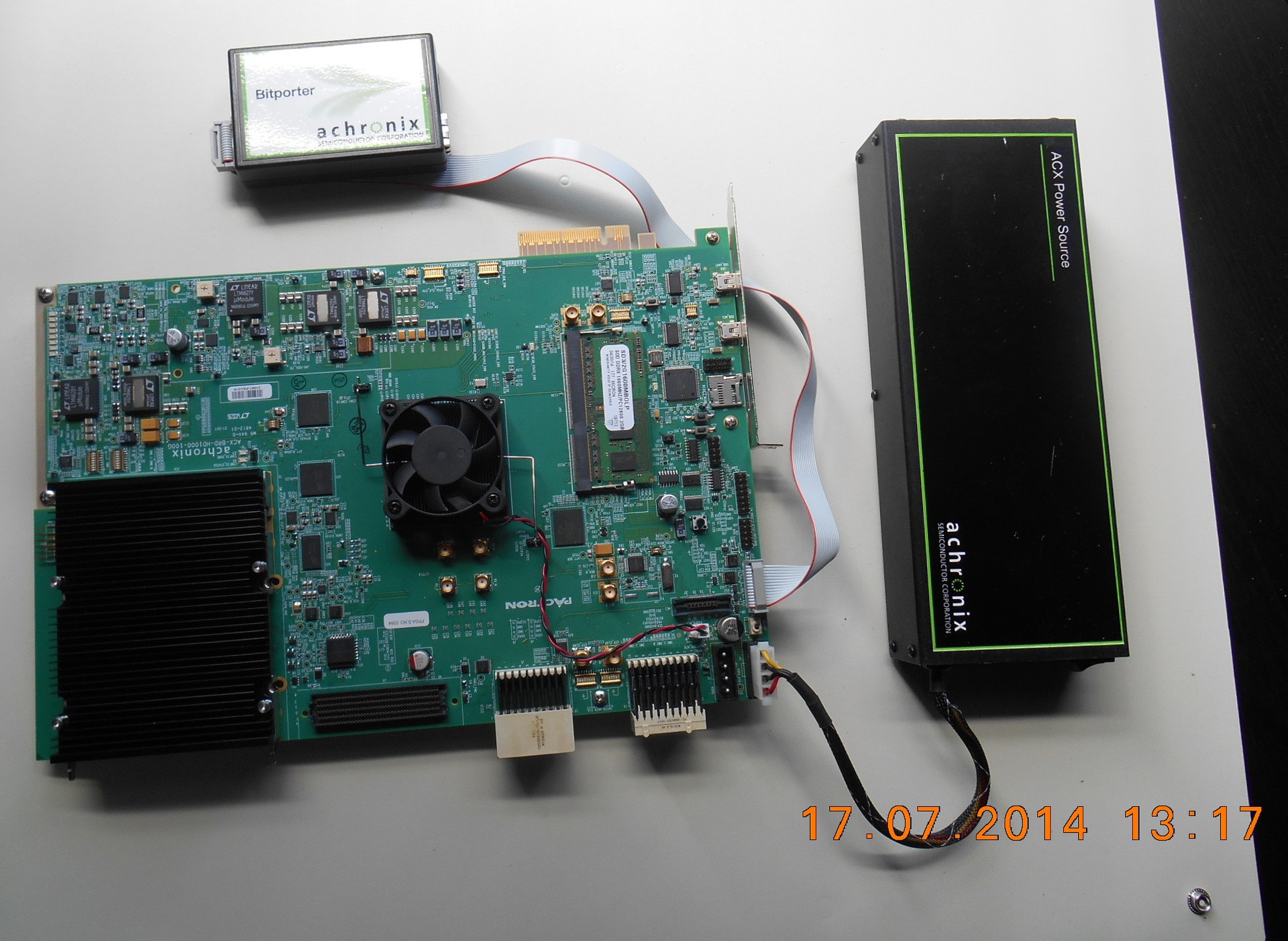
As you can see, the board itself is a complex and multifunctional product. The electrical circuit alone takes 90 pages! Therefore, it is not surprising that the board allows you to develop and debug, I am not afraid of this word, unique projects, for example, to create equipment for Ethernet 100G networks, for which there is a connector for the CFP module (the “black square” in the lower left corner in the photo above). Two Interlaken interfaces are routed to AirMax connectors.
Most struck by the thickness of the printed circuit board. How many layers are there? 20? thirty? 40? The question remained unresolved.
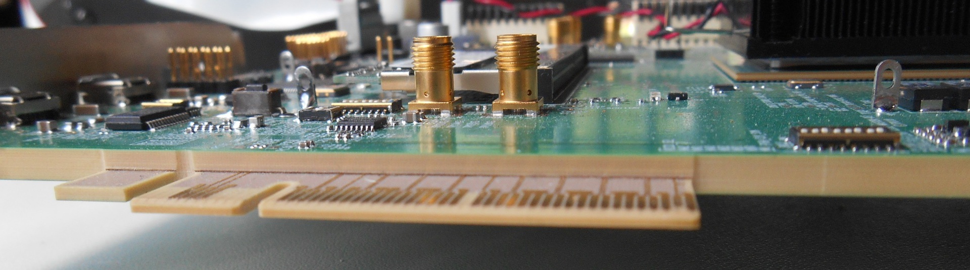
The board has a PCI-express connector (Gen 3 x8, 64 Gb / s) and can work as a peripheral device as part of a computer. Together, it looks like this:

The package includes a JTAG cable that acts as a loader and debugger. A feature of this cable is the ability to work through a USB port, or via Ethernet. In the latter case, you can organize remote access to the device. When working via Ethernet, an external power supply is required (supplied). Also included in the package is a powerful power source for the board itself and a 2GB DDR-3 RAM module.
Health Check
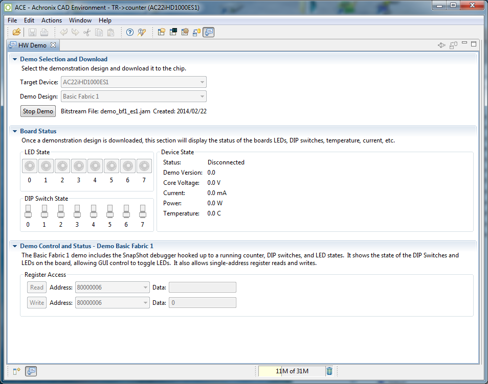
It turned out to be very simple to verify that the board is functioning, as A test is already built into the ACE shell for it. Therefore, the whole check, in fact, boils down to pressing a single button to download a test firmware. After that, you can play with the switches, turning the LEDs on and off and test the internal memory blocks. The board must be connected with a USB cable to the computer.
Development
And now - about how I did my first project for Achronix FPGAs. As such, the simplest option was chosen - a counter with the output of high-order bits to LEDs. Of course, such a simple project will not impress professionals, but it allows you to study the basic functionality of development tools used to work with FPGA Achronix and master the design route. In future publications, I plan to talk about more complex things, such as configuring and using hardware cores and implementing systems on a chip using the ARM processor core.
Project structure
Each project I place in a separate directory containing at least 3 subdirectories:
- Src - for source
- Syn - for synthesis
- TR - for implementation
Practice has shown that it is better not to keep anything superfluous in the Syn directory, because the synthesizer can wipe files placed there. Therefore, I store the source texts (I prefer to work in Verilog) in the Src directory, and all scripts in the TR directory
Source code
The source code of the module is completely straightforward:
module counter #( parameter CNT_WIDTH = 32 ) //   8 <= CNT_WIDTH
(
    input  wire             clk,
    input  wire             rstn,
    output wire [7:0]       leds
);
    wire                rst;
    reg [CNT_WIDTH-1:0] cnt;
    assign rst = ~rstn;
    always @(posedge clk or posedge rst)
        if (rst)    cnt <=  'h0;
        else        cnt <=  cnt+1;
    assign leds[7:0] = cnt[CNT_WIDTH-1: CNT_WIDTH-8];
endmodule
But for implementation on the demo board it needs to be slightly modified.
First, you need to select and properly connect the clock source. There are several of them on the board. After studying, a source with a frequency of 100 MHz having a differential output was selected. Therefore, it was necessary to add a differential buffer to the input clock circuit.
Secondly, I would like to see the internal signals in the process. All FPGA manufacturers have such an opportunity; it is also available in Achronix FPGAs. The internal signal analyzer is called SnapShot. Unlike competitors, the SnapShot component must be explicitly described in the design. This initially made me inconvenient, but then I appreciated the advantage of this approach. This advantage is in complete control over what you are doing. In addition, this approach allows you to very flexibly configure triggers to record monitored events.
So, in the final version, we have a differential clock input and a buffer for it, as well as a ShapShot component for studying internal signals. Final Verilog text:
`define USE_SNAPSHOT
module counter #( parameter CNT_WIDTH = 30 ) //   8 <= CNT_WIDTH <= MNTR_WIDTH
(
 `ifdef USE_SNAPSHOT
    input  wire             tck,
    input  wire             trstn,
    input  wire             tms,
    input  wire             tdi,
    output wire             tdo,
 `endif
    input  wire             clk_p,
    input  wire             clk_n,
    input  wire             rstn,
    output wire [7:0]       leds
);
//**********************************************
    wire                clk;
    wire                rst;
    reg [CNT_WIDTH-1:0] cnt;
    assign rst = ~rstn;
    IPAD_DIFF #( .odt("on"), .termination("100") )
    synth_clk_pad ( .pad(clk_p), .padn(clk_n), .dout(clk) );
    always @(posedge clk or posedge rst)
        if (rst)    cnt <=  'h0;
        else        cnt <=  cnt+1;
    assign leds[7:0] = cnt[CNT_WIDTH-1: CNT_WIDTH-8];
//*********************************************
`ifdef USE_SNAPSHOT
    localparam MNTR_WIDTH = 36;
    wire [MNTR_WIDTH: 0]        ss_zeroes;      ///// Signals going to trigger-detector block to do pattern matching
    wire                        ss_clk;
    wire [MNTR_WIDTH-1 :0]      ss_monitor_ch;  /// Signals monitored in Snapshot
    wire [MNTR_WIDTH-1: 0]      ss_trigger_ch;  ///// Signals going to trigger-detector block to do pattern matching
    wire                        ss_rstn_out;    ///// Active low user reset signal.
    wire                        ss_Arm;         ///// Indicates Snapshot activity.
    wire [MNTR_WIDTH-1:0]       ss_Stimuli;     ///// User specified values for 3rd trigger pattern value
    assign ss_clk   = clk;
    assign ss_zeroes = {MNTR_WIDTH+1{1'b0}};    ////
//////// Now Snapshot macro block instantiation ///////
    ACX_SNAPSHOT #(.MNTR_WIDTH(MNTR_WIDTH) )
    snapshot_0 (
        .tck        ( tck           ),
        .tms        ( tms           ),
        .trstn      ( trstn         ),
        .tdi        ( tdi           ),
        .tdo        ( tdo           ),
        .usr_clk    ( ss_clk        ),
        .Monitor_ch ( ss_monitor_ch ),
        .trigger_ch ( ss_trigger_ch ),
        .Rstn_out   ( ss_rstn_out   ),
        .Arm        ( ss_Arm        ),
        .Stimuli    ( ss_Stimuli    )
    );
    assign  ss_monitor_ch   = { ss_zeroes[MNTR_WIDTH-1: CNT_WIDTH], cnt[CNT_WIDTH-1:0] };
    assign  ss_trigger_ch   = ss_monitor_ch;
 `endif
//**********************************************
endmodule
Synthesis
To work, the Synplify synthesizer requires, in addition to the source texts and links to the library of elements, a constant file (usually it has the extension .sdc). Although not required for such a simple design, it is better to specify it. In such a simple case as ours, you only need to specify the names of the clock signal and their parameters.
# synplify_constraints.sdc
set_hierarchy_separator {/}
create_clock clk_p -period 10
create_clock tck -period 40
set_clock_groups -asynchronous -group { tck } -group { clk_p }
Next, create a project for Synplify, specify the files and libraries required for the synthesis, and start the process. If everything is done correctly, we get the output file with the extension .vma. (FPGA-design “gurus” may indicate that the main output format of Synplify is edif. But ACE accepts only Verilog netlist, which just have the .vma extension).
Implementation
Actually, the implementation process is carried out according to the standard scheme:
- Creating a project for ACE
- Specify the synthesis result file in the project (with the extension .vma)
- Define Constraints
- We start the implementation process
- Get the file to upload to the FPGA
For implementation it is necessary to prepare two files of constants: for defining blocks and specifying pins. Their contents are shown in the table:
# Ace_constraints.pdc
create_clock clk_p -period 10
create_clock tck -period 40
set_clock_groups -asynchronous -group { tck } -group { clk_p }
# io_preplacement.pdc
set_placement -batch -fixed {p:clk_p} {b:P19}
set_placement -batch -fixed {p:clk_n} {b:P18}
set_placement -batch -fixed {p:rstn} {b:P17}
set_placement -batch -fixed {p:leds[0]} {b:AE47}
set_placement -batch -fixed {p:leds[1]} {b:AJ46}
set_placement -batch -fixed {p:leds[2]} {b:AC46}
set_placement -batch -fixed {p:leds[3]} {b:AF47}
set_placement -batch -fixed {p:leds[4]} {b:AF46}
set_placement -batch -fixed {p:leds[5]} {b:AJ47}
set_placement -batch -fixed {p:leds[6]} {b:AG46}
set_placement -batch -fixed {p:leds[7]} {b:AE46}
On the computer, the implementation phase is as follows:
Design loading and debugging
To download the firmware file created in the previous step, go to the “Download” window, click on the “Run 'Program” button and wait a couple of minutes.
After the download is complete, the FPGA immediately starts working and we can observe a line of fun blinking LEDs on the board.
To view the internal signals connected to the SnapShot module, you need to open the “Snapshot debugger” window. In this window, you can configure the capture trigger modes and other parameters. The analysis is started with the “Arm” button, after which the tracking of the trigger state begins. After setting the trigger, a temporary diagram of the registered signals appears on the screen (with a slight delay).
Conclusion and Conclusions
In a short time, Achronix managed to create interesting, competitive FPGAs of the HI-END segment and development tools for them. The technology of working with them will not cause problems even for specialists of average qualification. Achronix products are already available in Russia.
References
- Website of the Russian Representative Office (“Laboratory of High Throughput VLSI”), url: www.achronix.ru
- Wikipedia, Acronix company article, url: en.wikipedia.org/wiki/Achronix
- Speedster22i HD family, datasheet, url: www.achronix.com/wp-content/uploads/docs/Speedster22iHD_FPGA_Family_DS004.pdf
- Developer Kit User Guide: Speedster22i HD1000 Development Kit User Guide, url: www.achronix.com/wp-content/uploads/docs/Speedster22i_DevelopmentKit_User_Guide_UG034.pdf
- SnapShot Debugger User Guide: www.achronix.com/wp-content/uploads/docs/Speedster22i_Snapshot_User_Guide_UG016.pdf
- Schematic diagram of the circuit board: 22iHD1000_Development_Board_Schematic.pdf
- Achronix company website (in English), url: www.acronix.com