JTAG interface? - It is very simple.
- From the sandbox
- Tutorial
Many are familiar with the word "JTAG", but the acquaintance is most likely superficial. In this article I want to take you to a new level, so to speak, "in the friend zone." Perhaps for many I will not discover anything new, but I hope it will be interesting to those who have long wanted to get acquainted. So, from the screw.
In 1985, a group of electronics manufacturers was formed - JTAG (Joint Test Action Group). To solve testing problems, an industry standard was put forward in 1990 - the IEEE Std 1149.1-1990 specification (IEEE Standard Test Access Port and Boundary-Scan Architecture). In the same year, Intel introduced the first processor with JTAG - 80486. Since then, the standard has been constantly updated and, at the moment, the latest version dates from 2013.
“And what are these problems with testing?”, You ask. Well then! It’s not much fun to jump with the oscilloscope over the terminals of the microcircuit, especially if there are many more than two of them! The standard allows you to greatly simplify life by embedding a special architecture in modern chips, providing access to pins (more precisely, to special I / O blocks) using a 4-wire serial interface. This architecture allows not only to control their condition, but also to manage them. Thus, you can do without bulky probes with physical contact and enjoy all the charm of the stage of debugging digital microcircuits or devices at the circuit board level.
The standard is used both for in-circuit programming and program debugging, and when working with packaged circuits. It is also used to check the quality of the soldering of microcircuits to the board, interboard and rack mounting of boards and blocks. I also need to say thanks to him for restoring inadvertently mobile devices.
The boundary scanning mechanism is enclosed, just in a shift register (Boundary Scan), connected between the terminals of the microcircuit and the core, and the multiplexer which connects this register at the right time. Each specific conclusion corresponds to the so-called "cells".

The cell includes one trigger of the boundary scan register and data selection multiplexer. Cells can be of different types depending on the output of the microcircuit and interface commands, i.e. depends on the manufacturer of a particular chip. Manufacturers do not adhere strictly to the standard and, therefore, a lot of modifications have divorced.
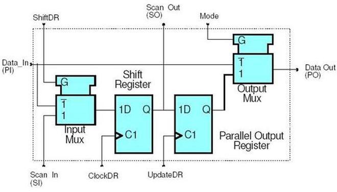
The figure shows one of the varieties of the cell. PI, PO - parallel input and output, SI, SO - serial.
The signals go to the microcircuit register through a multiplexer, which allows reading both the state of the microcircuit pins (INTEST instruction) and data coming from the outside to the shift register (EXTEST instruction). Varieties of instructions and their functionality again change from the desires of the manufacturer, but there are so-called mandatory:
As mentioned above, the JTAG interface has the following signal lines:
JTAG - synchronous interface, signals are received on the leading edge of the clock pulses with the least significant bits forward and only during the states of the TAP controller Shift-DR \ Shift-IR. The output is pushed to the trailing edge.
We got to the very core of JTAG, namely, the machine that controls the work. With its help, in fact, everything lives around. The machine has 16 states. The interface is controlled by acting on the machine through a TMS signal. Transitions occur on the rising edge of the TCK signal. Reading and writing data occurs simultaneously. Below is an illustration of the work taken from the documentation of Altera microcircuits.

Transition diagram of the automaton controlling the TAP modes
Transition diagram states:
The initial state in which the machine is located after switching on is Test-Logic Reset. As long as the TMS signal is set to “log.1”, the state of the machine remains unchanged. In this state, by default, the IDCODE or BYPASS statement is selected.
The reset signal TRST is optional, therefore, to reset the machine to its original state, use the following procedure. It is necessary to apply a high level signal to the TMS input and hold it for at least 5 TCK clock cycles. If the TMS signal is set by the host to a low level, the machine will go to the Run-Test / Idle state (active state in which nothing happens). Usually, from this state you can switch to the Select-IR state in order to load a new instruction into the controller. But if the input of the TMS signal is not affected by the signal from the host, but by a low level interference, then, as in the previous case, the machine will switch to the Run-Test / Idle state. If the short-term interference (lasting no more than one period of synchronization frequency) ceases, then the machine will again return to its original state after three clock cycles - Test-Logic Reset.
To load a new command into the controller, it is necessary to transfer the machine from the Run-Test / Idle state to the Select-IR, Capture-IR, Shift-IR state. Then you need to “push” a new command into the data chain, and then transfer the machine through the states Exit1-IR, Update-IR and again to Run-Test / Idle. The logic of working with data is the same. Keep in mind that a high-level signal during transition from the Shift-IR \ DR states is supplied along with the last bit of information.
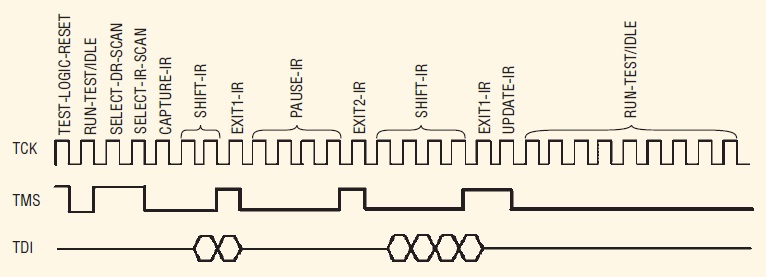
Signal diagram during transitions for loading a command
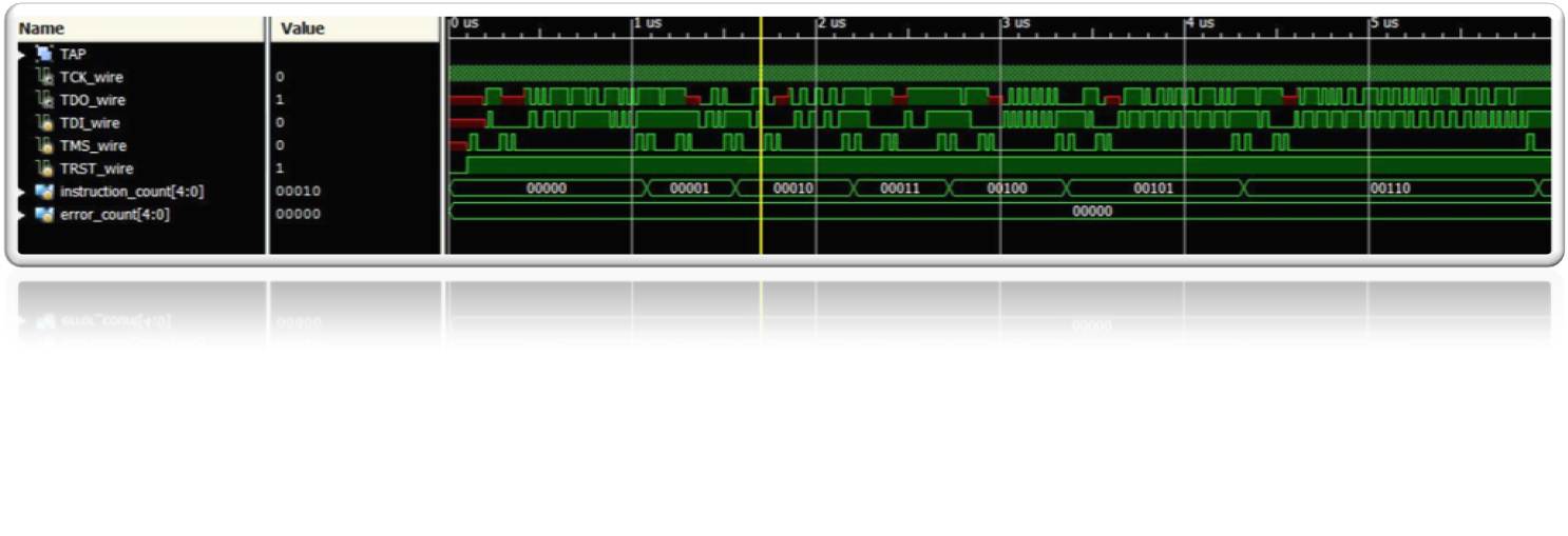
If you write JTAG code on Verilog using a specialized CAD system, the resulting diagram will look something like this:

Link to dropbox, full size image
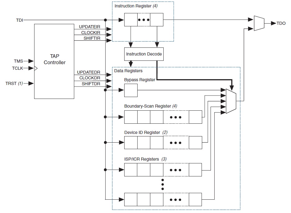
Finally, you can show the complete block diagram of the JTAG device and you should understand it :
Using JTAG and edge scanning technology in a microchip, on a board or in a device adds value and increases project development time. But, nevertheless, these costs are easily paid back during testing, which is provided at each stage of the product’s life cycle. What was originally developed as a production testing tool is used before the start of production, during mass production and after production, that is, during the operation phase by the end user. In addition to directly boundary testing, designers use JTAG technology to perform self-testing (BIST) (in those components where it is implemented) and load internal values into device registers or program ROM chips. Tests that were developed and used at the design stage,
The use of boundary scanning during the operation of the product also gives a certain positive effect. Operational failures often occur due to structural failures that are caused by elevated temperature, humidity, and vibration. Using boundary scanning, technicians are able to quickly check the product for structural errors up to the level of components without laborious research or returning the board to the manufacturer.
References:
Wiki
Boundary-scan in Altera devices
off. Page Working Group 1149.1 standard, the IEEE
1149.1-2013 - the IEEE for the Test of Standard the Access Port and Boundary-the Scan Architecture
Good Habr article which affected JTAG testing
release EEVblog about JTAG by Killy
The article used some data from the journal "Modern Electronics" issue number 2 2007.
Introduction
In 1985, a group of electronics manufacturers was formed - JTAG (Joint Test Action Group). To solve testing problems, an industry standard was put forward in 1990 - the IEEE Std 1149.1-1990 specification (IEEE Standard Test Access Port and Boundary-Scan Architecture). In the same year, Intel introduced the first processor with JTAG - 80486. Since then, the standard has been constantly updated and, at the moment, the latest version dates from 2013.
“And what are these problems with testing?”, You ask. Well then! It’s not much fun to jump with the oscilloscope over the terminals of the microcircuit, especially if there are many more than two of them! The standard allows you to greatly simplify life by embedding a special architecture in modern chips, providing access to pins (more precisely, to special I / O blocks) using a 4-wire serial interface. This architecture allows not only to control their condition, but also to manage them. Thus, you can do without bulky probes with physical contact and enjoy all the charm of the stage of debugging digital microcircuits or devices at the circuit board level.
The standard is used both for in-circuit programming and program debugging, and when working with packaged circuits. It is also used to check the quality of the soldering of microcircuits to the board, interboard and rack mounting of boards and blocks. I also need to say thanks to him for restoring inadvertently mobile devices.
And how does it work?
The boundary scanning mechanism is enclosed, just in a shift register (Boundary Scan), connected between the terminals of the microcircuit and the core, and the multiplexer which connects this register at the right time. Each specific conclusion corresponds to the so-called "cells".
The cell includes one trigger of the boundary scan register and data selection multiplexer. Cells can be of different types depending on the output of the microcircuit and interface commands, i.e. depends on the manufacturer of a particular chip. Manufacturers do not adhere strictly to the standard and, therefore, a lot of modifications have divorced.
The figure shows one of the varieties of the cell. PI, PO - parallel input and output, SI, SO - serial.
The signals go to the microcircuit register through a multiplexer, which allows reading both the state of the microcircuit pins (INTEST instruction) and data coming from the outside to the shift register (EXTEST instruction). Varieties of instructions and their functionality again change from the desires of the manufacturer, but there are so-called mandatory:
- EXTEST is an instruction that allows, by setting logical values on the working contacts of electronic components, to check external circuits that are directly related to the component under test.
- INTEST - instruction provides the ability to set logical values inside the chip, that is, at the inputs of the kernel, thereby checking it.
- SAMPLE_PRELOAD - allows you to test the core of an electronic element in static mode, setting the values of logical levels on the border of its output buffers.
- BYPASS - an instruction in which our boundary scan register "collapses" into one trigger. In this case, the data from the input (TDI) to the output (TDO) is transmitted with a delay of one clock clock interface frequency (TCK). This mode allows you to effectively use the capabilities of the serial interface when organizing long sequentially combined chains.
- IDCODE - the instruction outputs the value of the built-in 32-bit register with the identifiers of the manufacturer, model and version of the device.
Interface Signal Lines
As mentioned above, the JTAG interface has the following signal lines:
- TDI - Test Data Input - data input signal, data is shifted along the rising edge of TCK.
- TDO - Test Data Output - serial data output JTAG, advanced on the trailing edge of the TCK, should be in the third state - Z - when data is not transmitted.
- TMS - Test Mode Select - control signal of the TAP - controller.
- TRST - Test Reset - is not always there, since a reset can be achieved by holding TMS = 1 for a while, the active signal level is 0.
- TCK - Test Clock - clock frequency.
JTAG - synchronous interface, signals are received on the leading edge of the clock pulses with the least significant bits forward and only during the states of the TAP controller Shift-DR \ Shift-IR. The output is pushed to the trailing edge.
TAP - controller
We got to the very core of JTAG, namely, the machine that controls the work. With its help, in fact, everything lives around. The machine has 16 states. The interface is controlled by acting on the machine through a TMS signal. Transitions occur on the rising edge of the TCK signal. Reading and writing data occurs simultaneously. Below is an illustration of the work taken from the documentation of Altera microcircuits.
Transition diagram of the automaton controlling the TAP modes
Transition diagram states:
- Test-Logic-Reset - initial state;
- Run-Test / Idle - the transition state of the controller when performing tests or waiting for the next
- teams
- Select-IR, Select-DR - the state after which testing of commands and data will be performed;
- Capture-IR, Capture-DR - state of receiving commands, data;
- Shift-IR, Shift-DR - shift status of commands, data;
- Exit1-IR, Exit2-IR - exit from the mode of working with commands;
- Exit1-DR, Exit2-DR - exit from data mode;
- Pause-IR, Pause-DR - pause state;
- Update-IR, Update-DR - state of overwriting data in output registers.
The initial state in which the machine is located after switching on is Test-Logic Reset. As long as the TMS signal is set to “log.1”, the state of the machine remains unchanged. In this state, by default, the IDCODE or BYPASS statement is selected.
The reset signal TRST is optional, therefore, to reset the machine to its original state, use the following procedure. It is necessary to apply a high level signal to the TMS input and hold it for at least 5 TCK clock cycles. If the TMS signal is set by the host to a low level, the machine will go to the Run-Test / Idle state (active state in which nothing happens). Usually, from this state you can switch to the Select-IR state in order to load a new instruction into the controller. But if the input of the TMS signal is not affected by the signal from the host, but by a low level interference, then, as in the previous case, the machine will switch to the Run-Test / Idle state. If the short-term interference (lasting no more than one period of synchronization frequency) ceases, then the machine will again return to its original state after three clock cycles - Test-Logic Reset.
To load a new command into the controller, it is necessary to transfer the machine from the Run-Test / Idle state to the Select-IR, Capture-IR, Shift-IR state. Then you need to “push” a new command into the data chain, and then transfer the machine through the states Exit1-IR, Update-IR and again to Run-Test / Idle. The logic of working with data is the same. Keep in mind that a high-level signal during transition from the Shift-IR \ DR states is supplied along with the last bit of information.
Signal diagram during transitions for loading a command
If you write JTAG code on Verilog using a specialized CAD system, the resulting diagram will look something like this:
Link to dropbox, full size image
Finally, you can show the complete block diagram of the JTAG device and you should understand it :
… In conclusion...
Using JTAG and edge scanning technology in a microchip, on a board or in a device adds value and increases project development time. But, nevertheless, these costs are easily paid back during testing, which is provided at each stage of the product’s life cycle. What was originally developed as a production testing tool is used before the start of production, during mass production and after production, that is, during the operation phase by the end user. In addition to directly boundary testing, designers use JTAG technology to perform self-testing (BIST) (in those components where it is implemented) and load internal values into device registers or program ROM chips. Tests that were developed and used at the design stage,
The use of boundary scanning during the operation of the product also gives a certain positive effect. Operational failures often occur due to structural failures that are caused by elevated temperature, humidity, and vibration. Using boundary scanning, technicians are able to quickly check the product for structural errors up to the level of components without laborious research or returning the board to the manufacturer.
References:
Wiki
Boundary-scan in Altera devices
off. Page Working Group 1149.1 standard, the IEEE
1149.1-2013 - the IEEE for the Test of Standard the Access Port and Boundary-the Scan Architecture
Good Habr article which affected JTAG testing
release EEVblog about JTAG by Killy
The article used some data from the journal "Modern Electronics" issue number 2 2007.