Hf2Te2P - "silicon" quantum computers?

Apparently the day does not pass without someone talking about quantum computers. This technology promises us devices that operate on the “faster, higher, stronger” principle, while it is difficult to fully describe all its advantages and disadvantages. However, the prospect of incredibly fast calculations and data transfer, as well as storing a huge amount of data “in the poppy seed” is undoubtedly attractive. And to achieve so desirable heights, a lot of work is needed, because new technology is new principles, new devices and, of course, new materials. Classic, as it is now called, computers use silicon as a base material. What do quantum ones use? This will be discussed in the study we are considering today. What are these new properties already known substances Why did they pay attention to him, and why was he called “a breakthrough” in quantum technologies? The answers are hidden in the scientists report. It remains only to find them. Go.
Background and Basis of Research The
discovery of topological insulators * has become a huge incentive to re-examine various substances with a desire to find properties useful for quantum technologies in them . Such materials were first described in the 80s, but they were only really found in the recent 2007.
Topological insulator * (TI) - material, the inner part of which is an insulator, and the surface conducts electrical current.These materials have pushed scientists to investigate non-standard surface states * of substances already known and definitely useful for quantum computers.
Surface state * is the electronic state of a solid surface.Surface states characteristic of topological insulators may have different origins, for example, strong spin-orbit interaction * or the effect of electron correlation. In any case, if we understand the origin of such states, then we can use them in the implementation of such a large-scale and ambitious project as quantum technologies.
Spin-orbit interaction * - the interaction of a moving particle and its own magnetic moment, caused by the spin of this particle.The first representative of TI was the compound of bismuth, tellurium and sulfur, known as tetradimite (Bi 2 Te 2 S). The surface state of tetradimite was based on spin-orbit interaction and was supported by m-symmetry * .
T-symmetry * is the symmetry of equations with respect to time reversal (i.e., replacing time t with -t ).Also worth mentioning are Dirac topological semimetals, such as Cd 3 As 2 and Na 3 Bi. They discovered a connection between the valence zone * and the conduction band * at certain discrete points of the Brillouin zone * .
Valence band * is the energy zone of the electronic state of a solid, filled with valence electrons and responsible for the electrical conductivity of the body.
The conduction band * is the energy band of the electron state of a solid, unfilled with electrons.When electrons from the valence band pass into the conduction band, having passed the forbidden band, they begin to move under the influence of an electric field, i.e. participate in conduction.
Brillouin zone *Crystal and inversion symmetry are present in these materials.
a) - for a simple cubic lattice;
b) - for the hexagonal grid.

A very interesting situation was associated with another semi-metal, tantalum arsenide (Weyl semi-metal). As early as 1929, Hermann Weyl formulated the equation of motion for a massless two-component particle, named after him. Being engaged in this, the scientist predicted the existence of the so-called Weyl fermion. Up until 2015, no one was able to obtain the Weyl semimetal, and therefore fix the particle predicted by him with a half-integer spin value. When x-ray and ultraviolet rays were passed through the crystal of tantalum arsenide, scientists were able to study the physical properties of an unusual substance. Lattice excitations that manifest themselves as Weyl fermions were discovered.
Weyl's fermions are surprising in that, unlike electrons, they are not subject to backscattering when a particle encounters an obstacle. Weil particles simply pass through or flow around an obstacle, as if it is not for them at all.
Such materials arouse the keen interest of scientists, because they can drastically change the world of computer technology due to their extraordinary properties.
As we see, it is quite enough and the above materials for implementation in quantum technologies. However, the goal of our heroes today was not just to find the right material, but truly the ideal, combining several important properties in oneself.
Metal Hf 2 Te 2 P became such a substance .in which topological fermionic surface states, the Dirac intersection and the Dirac arc were found. Very impressive mixture in one bottle.
Experimental Measurements
Angular-resolution photoelectron spectroscopy served as the primary method for detecting all of the above.
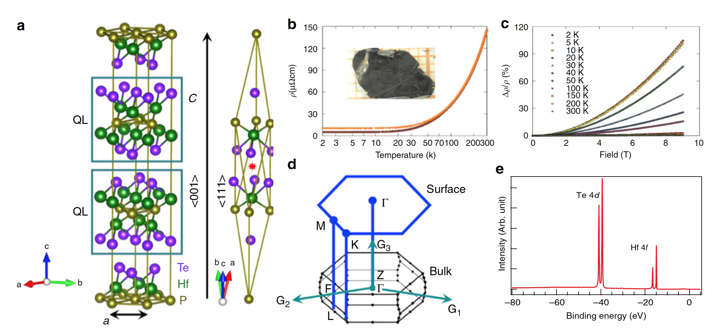
Image No. 1: Crystal structure and characterization of the Hf 2 Te 2 P sample.
Image 1a shows the rhombohedral tetradimite crystal structure of Hf 2 Te 2 P. The squares are divided into 2 groups of the densest five-layer packing of atoms * . The red star indicates the center of inversion * . Violet dots areTe (tellurium), green - Hf (hafnium), and yellow - P (phosphorus).
An example of the closest packing of atoms.
Inversion * - space transformation equivalent to the mathematical concept of "reflection".Graph 1b displays the temperature dependence of the electrical resistance measured in a single Hf 2 Te 2 P crystal when exposed to a magnetic field perpendicular to the current flowing in the basal plane of the crystallographic unit cell. The brown line is a 0 T magnetic field; the orange line is a magnetic field of 9 T.
Also on the graph 1b we see the image of a single crystal * Hf 2 Te 2 P grown for this study.
A single crystal * is a separate crystal with a continuous crystal lattice.Graph 1c displays the dependence of the magnetoresistance at different temperatures in a single crystal of Hf 2 Te 2 P, when the current flows in the basal plane of the crystallographic unit cell.
The projection of the volume Brillouin zone on the hexagonal surface of the same zone of the Hf 2 Te 2 P crystal , where points of high symmetry are marked, is shown in Figure 1d .
Finally, image 1e shows the results of measurements of the level of the Hf 2 Te 2 P core . Here we see large peaks of Te 4d (tellurium) and Hf 4f (hafnium), which is an indicator of the high quality of the test sample.
In addition to defining several Dirac cones * at point Γ (image 1d ) at different levels of binding energy * below and above the Fermi level * , the Dirac arc was also detected, centralized at point M along the G-M-D direction in the energy pulse plane.
Dirac Cones *
Fermi level * - increase in the energy of the ground state of the system with the addition of 1 particle; the maximum fermion energy in the ground state at an absolute zero temperature.
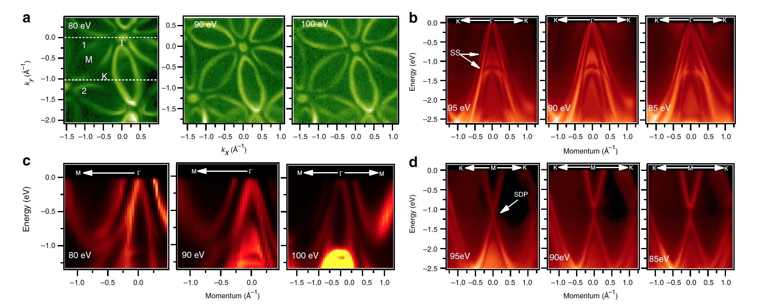
Image # 2: The Fermi surface and the observation of multiple fermion states
The images in group 2a show different Fermi surfaces with different levels of photon energy (80 eV, 90 eV and 100 eV). White dotted lines numbered 1 and 2 indicate the direction of dispersion.
Images from b to d show dispersion maps, measured along different highly symmetrical directions with different levels of photon energy. The data were obtained using an experimental station of a source of synchrotron radiation * at a temperature of 18 K (-255.15 ° C).
Synchrotron radiation * is electromagnetic radiation emitted by charged particles moving at relativistic speeds along trajectories bent by a magnetic field.
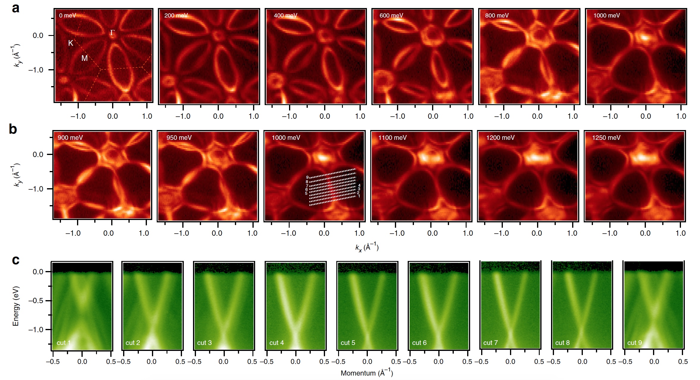
Image number 3: Experimental observations of the arc of Dirac.
The images of group 3a show the contours of the constant-energy surface at various indicators of the binding energy (from 0 to 1000 meV, millielectronvolt). The Fermi surface is clearly visible in the form of a flower with six petals, suggesting that such a pronounced dispersion is possible even in a metallic Dirac material. Below, at 3b , the contours of the constant energy are shown closer to the Dirac arc.
3c is the dispersion map in the KMK direction along the cut direction, revealed for the constant energy surface at a binding energy level of about 1000 meV.
Approaching the summing up, it is worth noting all the fermion states defined in the sample through calculations and experimental observations.

Image 4: multiple fermion states.
Summarizing
As it was said earlier, one of the most important observations was the Fermi surface in the form of a flower with six petals, suggesting that even in a metallic Dirac material so pronounced dispersion is possible. The Dirac cones with linear dispersion in a wide energy range (~ 2.3 eV), which is larger than that of ZrSiS (~ 2 eV), have the same importance.
It should be noted that in the already well-studied topological insulators of the n-type Bi 2 Se 3 / Bi 2 Te 3 (5a ) it was experimentally found that the lower and upper Dirac surface cones have a Fermi level well above the Dirac point (the contact point of the valence band and the conduction band). In the case of Sb 2 Te 3 , a p-type material, the Dirac point is located much higher than the Fermi level ( 5b ). In some other materials, contact between bulk conductance and the valence zone is observed in a one-dimensional loop protected by asymmetric symmetry ( 5c ).
And all these three phenomena are found in one material at once, in Hf 2 Te 2 P ( 5d , 5e ). Until this moment, no material could boast of such.
For acquaintance with details of calculations and measurements I strongly recommend to read the report of researchers available on this link.
The researchers also provided access for everyone to additional materials of their work.
Epilogue
Such studies can in no way be called simple. Quantum technology is generally difficult to call easy, at least to me. However, such a colossal work can pay off in a hundredfold, since previously hidden properties of a known material discovered by researchers can expand the range of possibilities in the implementation of quantum computers. The combination of several useful properties in one material can be an advantage over the complexity of its manufacture. Perhaps, if someone does not succeed in finding an alternative to the above-described material, he may become the Rosetta stone of the technologies of the future. All these studies, although supported by experimental measurements and observations, still remain largely theoretical. Only the practical implementation of any device using such materials will be able to 100% assure us of its uniqueness and incredible usefulness, as scientists say. In any case, no need to hurry. The long way still needs to be overcome by the world of science, so that such studies go down in history as the discoveries of the past that influenced our future.
Thank you for staying with us. Do you like our articles? Want to see more interesting materials? Support us by placing an order or recommending to friends, 30% discount for Habr users on a unique analogue of the entry-level servers that we invented for you: The whole truth about VPS (KVM) E5-2650 v4 (6 Cores) 10GB DDR4 240GB SSD 1Gbps from $ 20 or how to share the server? (Options are available with RAID1 and RAID10, up to 24 cores and up to 40GB DDR4).
Dell R730xd 2 times cheaper? Only we have 2 x Intel Dodeca-Core Xeon E5-2650v4 128GB DDR4 6x480GB SSD 1Gbps 100 TV from $ 249 in the Netherlands and the USA! Read about How to build an infrastructure building. class c using servers Dell R730xd E5-2650 v4 worth 9000 euros for a penny?