China Institute of Microelectronics creates 22nm transistors
 The Institute of Microelectronics of the Chinese Academy of Sciences (IMECAS) announced that they were able to create a transistor with a gate length of 22nm (for comparison, 22nm transistors in Intel processors have a gate length of 26nm). Transistors use a metal gate and a high-k gate gate dielectric (necessary to reduce leakage current by tunneling electrons through an ultra-thin gate gate dielectric layer).
 Transistors do not use a “3-way gate” in the style of Intel, but more traditional planar gate-last transistors (when the gate is formed last).
The PRC initiated these studies in 2009 as one of the main national projects. According to IMECAS, the development of 22nm technology of integrated circuits in China will save huge amounts of money on currently imported technologies (or bargain for more favorable prices).
To understand the order of prices - Angstrom-T 130nm technology cost ~ 120 million euros (2007), 90nm Micron - about 27 million euros (2011, according to press reports). At finer rates, cost increases exponentially. Perhaps in the future, technology will have to be bought from China.

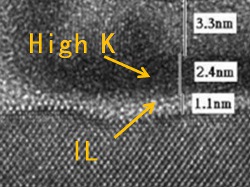
Separate silicon atoms (in the lower part of the image) are clearly visible. IL is an SiO 2 interface layer between silicon and a high-k HfO 2 dielectric (it does not directly adhere directly).

Light lines at an angle of 45 degrees in silicon is an artificially created defect in the crystal lattice to create a voltage of silicon in the transistor channel (this is necessary to increase its speed).