Overcoming Moore's Law: Transistor Technologies of the Future
We are talking about alternatives for silicon.

/ photo Laura Ockel Unsplash
Moore’s Law, Dennard’s regularity and Kumi’s rule lose their relevance. One of the reasons - silicon transistors are approaching their technological limit. We discussed this topic in detail in a previous post . Today we are talking about materials that in the future can replace silicon and extend the validity of the three laws, which means increasing the efficiency of processors and computing systems using them (including servers in data centers).
Carbon nanotubes
Carbon nanotubes are cylinders whose walls consist of a monatomic carbon layer. The radius of carbon atoms is smaller than that of silicon, so nanotube-based transistors have greater electron mobility and current density. As a result, the speed of the transistor increases and its power consumption decreases. According to engineers from the University of Wisconsin at Madison, productivity is up fivefold.
The fact that carbon nanotubes have better characteristics than silicon has been known for a long time - the first such transistors appeared more than 20 years ago. But only recently, scientists managed to circumvent a number of technological limitations in order to create a sufficiently effective device. Three years ago, physicists from the aforementioned University in Wisconsin presented a prototype of a nanotube-based transistor that outperformed modern silicon devices.
One of the applications of devices based on carbon nanotubes is called flexible electronics. But so far the technology has not gone beyond the laboratory and there is no question of its mass introduction.
Graphene nanoribbons
They are narrow strips of graphene several tens of nanometers wide and are considered one of the main materials for creating transistors of the future. The main property of graphene tape is the ability to accelerate the current flowing through it using a magnetic field. At the same time, graphene has 250 times greater electrical conductivity than silicon.
According to some reports , processors based on graphene transistors will be able to operate at frequencies close to terahertz. While the frequency of operation of modern chips is set in the range of 4-5 gigahertz.
The first prototypes of graphene transistors appeared ten years ago . Since then, engineers have been trying to optimize the processes of "assembly" of devices based on them. Most recently, the first results were obtained - a team of developers from the University of Cambridge in March announced the launch of the first graphene microcircuits . Engineers say that the new device can accelerate the work of electronic devices by ten times.
Hafnium dioxide and selenide
Hafnium dioxide has been used in the manufacture of microchips since 2007 . From it make an insulating layer on a transistor gate. But today, engineers suggest optimizing the operation of silicon transistors with it.

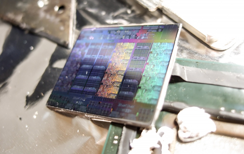
/ photo Fritzchens Fritz PD
At the beginning of last year, scientists from Stanford found that if the crystalline structure of hafnium dioxide was reorganized in a special way, its electric constant (responsible for the ability of the medium to transmit an electric field) would increase by more than four times. If you use such material when creating transistor gates, you can significantly reduce the effect of the tunneling effect .
Also american scientistsfound a way to reduce the size of modern transistors using hafnium and zirconium selenides. They can be used as an effective insulator for transistors instead of silicon oxide. Selenides have a significantly smaller thickness (three atoms), while maintaining a good band gap. This is an indicator that determines the power consumption of a transistor. Engineers have already managed to create several working prototypes of devices based on hafnium and zirconium selenides.
Now, engineers need to solve the problem with the connection of such transistors - to develop appropriate contacts for them in small sizes. Only after that it will be possible to talk about mass production.
Molybdenum disulfide
Molybdenum sulfide per se is a rather poor semiconductor, which is inferior in properties to silicon. But a group of physicists from the University of Notre Dame found that thin molybdenum films (one atom thick) have unique qualities - transistors based on them do not pass current in the off state and require little energy to switch. This allows them to work at low voltages.
The prototype of the molybdenum transistor was developed in the laboratory. Lawrence at Berkeley in 2016. The width of the device is only one nanometer. Engineers say such transistors will help extend Moore’s law.
Also, a transistor based on molybdenum disulfide last year was presented by engineers from a South Korean university. It is expected that the technology will find application in control circuits of OLED displays. However, there is no need to talk about the mass production of such transistors.
Despite this, researchers from Stanford argue that the modern infrastructure for the production of transistors can be restructured to work with molybdenum devices at minimal cost. Will it be possible to implement such projects, remains to be seen in the future.
What are we writing about in our Telegram channel:
- How IaaS Provider Protects Personal Data of Client Companies
- Following the VMware EMPOWER 2019 Event: Learning the Basics of Workspace ONE
- A year later - who received fines for GDPR
- What's up with data centers - new processors
- How are the data centers: technological trends in recent years
- How to protect an IoT network: open source will help
