Microelectronics technologies on the fingers: Moore’s Law, marketing moves and why nanometers are not the same now. Part 1
- Transfer
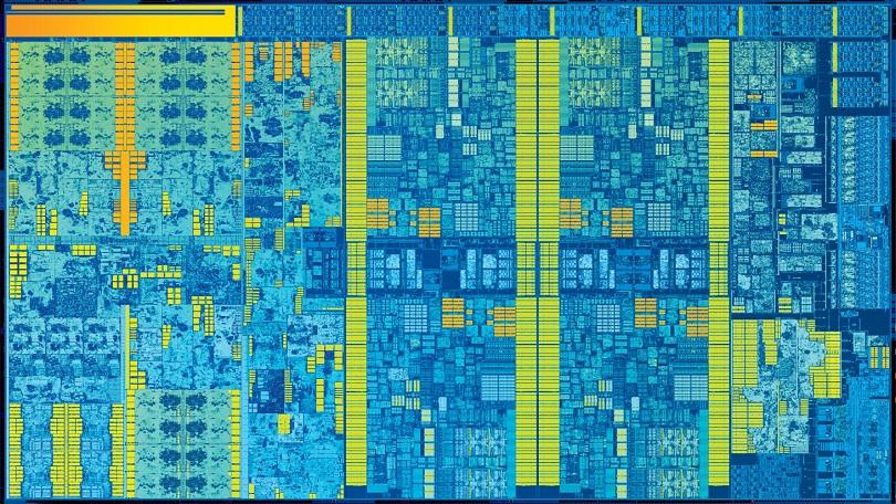
Possible photo of 10 nm IceLake. Source
Strange things are happening on the processor market. The world leader in the person of Intel has been struggling for the fifth year in attempts to switch to 10 nm manufacturing process. Initially, they announced the transition to 10 nm in 2015, then in 2016, 2017 ... In the yard of 2019, and 10 nm from Intel in the series is still not there. Well, no, there are some experimental / engineering samples, but a high yield is a problem. A real transition is expected no earlier than 2022 already.
Actually, this was the reason for the shortage of Intel processors in the market. To overcome it, the company expands the production of modified 14 nm processors (the same Lake only in profile) and even returns to 22 nm. It would seem that regression is obvious. At this time, Korean Samsung, Taiwanese TSMC, and AMD, which joined them with the ZEN 2 platform, are reporting on the introduction of as much as 7 nm and are about to switch to 5 nm. They took out the “Moore's Law” from the dusty cabinet and declared it more alive than all the living. Soon there will be 3 nm, and 2 nm, and even 1 nm ( sic! ) - pourquoi pas ?!
What happened? Really
Disclaimer: This articleI found it by accident and was extremely amazed at how competently and in detail the problems of modern microelectronics are revealed in it, in particular, the death of Moore's law and marketing. Once upon a time I myself dabbled in writing articles about chip making , and in the series of articles “Inside Look” I even looked inside of them, that is, The topic is extremely interesting to me. Naturally, I would like the author of the original article to publish it on Habré, but in connection with employment, he allowed me to transfer it here. Unfortunately, the Habr rules do not allow direct copy-paste, so I added links to sources, pictures and a little gag and tried to straighten the text a little bit. Yes, and articles ( 1 and 2 ) on this topic fromamartology know and respect.
So, let's sort out the problem together. We will try as much as possible to delve into physics and technology, and not delve into the nuances (of which the name is legion!). The description below is simplified and sometimes schematic. Write comments, we will try to constructively discuss.
Foreword
“Not everything is so straightforward ...” one officer’s daughter used to say. If you look at the density of transistors, then it is almost the same in 14 nm technology from Intel and 7 nm technology from TSMC ( ooops !!! ). And even Intel’s rollback to 22 nm didn’t have a big impact on performance. What the hell is this? By all rules, the transition from 14 nm to 7 nm technology should increase the density of transistors as much as 4 times. And this is according to the precepts of Gordon Moore, whose 50th anniversary of the law was celebrated recently, and on the nose is the 55th anniversary!
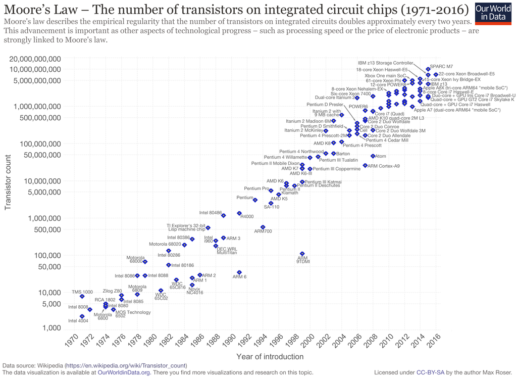
Moore's law cast in iron. As you can see, we are "marking time" in place already years 5. Source
At the same time, mixed statements are being made. Some argue that the "Law of Moore" is more relevant than ever, and microelectronics will develop as before. Brilliant scientists, designers and engineers will overcome any limitations, even the laws of physics. People require new achievements, and they will not take long.
Others say that all the guys have reached the physical limits, we will lick what is, but this is normal. This has long been warned. So the head of NVIDIA said during CES 2019 that Moore’s law is dead and now the vector (Huang should not be in the vector, but in the tensor) of development must be changed. The lithography specialist of AMD and GlobalFoundries agrees with him .
In fact, all these technological standards of units and tens of nanometers have long been divorced from physical dimensions and have become more elements of marketing. At least the last 15 years: after the transition from 130 nm to 90 nm. It was then that for the first time faced with limitations not technological, but basic physical. Experts, by the way, talked about this, but their quiet voice was drowned out by the bravura broadcasts of marketers who pretended that nothing had happened, that everything was going its own way, according to the precepts of
Unfortunately, for marketers, and perhaps fortunately for us, Moore’s law is not a law of nature, but an empirical observation formulated in 1965 by one of the founders of Intel, Gordon Moore. According to his observations, new series of microcircuits came out with an interval of a year, while the number of transistors in them grew by about 2 times. In 1975, the law was amended; according to it, doubling should occur every 24 months. Since then, for almost 40 years, Moore’s law has been elevated to the rank of an icon and a banner for manufacturers of digital microelectronics, which were sometimes twisted (24 months turned into 36, now stagnation - see the picture above).
Along the way, various technological limitations arose that slowed down the process (the same transition through the diffraction limit). Or breakthroughs that gave a sharp increase in miniaturization. For an outside observer, everything looked like stable growth in full compliance with Moore's law, and not least the efforts of marketers.
Physics of “His Majesty Silicon”
I'll start with silicon ode. Silicon is just heaven’s gift for microelectronics manufacturers. Not only that, literally, underfoot, silicon is also a good semiconductor with very suitable parameters (in terms of the combination of electrical, energy and physical characteristics). Pure silicon is almost a dielectric; conductivity is completely determined by the concentration of impurities. It has high thermal conductivity, is technologically advanced, and is resistant to aggressive environments.
Likbez for beginners
Silicon at ordinary temperatures is a semiconductor with a cubic crystal lattice. 4 external electrons of silicon atoms are "socialized", i.e. belong to all atoms of the crystal lattice. They are not free, but not rigidly attached to their atom. This is a feature of semiconductors. For a while, these electrons revolve around their atom, then are transferred to the neighboring one, and the neighboring ones come in their place. Thus, external (valence) electrons randomly travel from atom to atom throughout the crystal ( note: not quite so, the electrons themselves do not travel, they only transfer energy through interaction with each other) Occasionally, some kind of electron is completely detached from the atom and begins (quasi) to move freely between the crystal lattice. In its place remains a positive silicon ion with an unfilled electron vacancy - a “hole”. The next time the electrons are forwarded from a neighbor, the vacancy is filled, but it appears at the neighbor, then at his neighbor, etc. The hole also begins to travel randomly through the crystal.
If we now apply an electric field, then a free electron will fly from minus to plus. Valence electrons are also subject to the action of the field and begin to quickly fill vacancies toward the plus side, and hole vacancies will flow towards the minus side. This behavior looks like a hole is a free charge carrier, such a free electron, only with a positive charge. The behavior of the hole is described by the same formulas as the electron, corrected for a larger “ effective mass ”. Therefore, they often do not steam and, for simplicity, consider holes to be ordinary elementary particles with a positive charge.
At room temperature, one electron-hole pair per trillion silicon atoms (concentration 10 -12), pure silicon at room temperature is an insulator (conditionally: electrons and holes annihilate too quickly with each other, not having time to reach the end of the crystal).
If now an atom with 5 external electrons, for example, phosphorus, is introduced into the silicon lattice, then it is included in the 4-electron exchange, and the fifth electron becomes free. We obtain positive phosphorus ions and an “electron gas” embedded in silicon from free electrons. The conductivity of silicon with such an impurity increases linearly; concentrations of one phosphorus atom per million silicon atoms ( ppm ) already dramatically change the electrical properties. An admixture of phosphorus is called donor, and the semiconductor itself is called N-type conductivity . In addition to phosphorus, it can be arsenic or antimony.
Now we add to pure silicon atoms with 3 external electrons, for example, boron. It is also included in the 4-electron exchange, but can only give 3 electrons. At neighboring silicon atoms, a “hole” appears and sets off on a journey through the crystal. We get negative boron ions and a positively charged hole gas. Such an impurity is called acceptor, and the semiconductor is P-type . In addition to boron, acceptors are aluminum, gallium and indium.
By the way, extremely pure silicon (so that it is an insulator) is incredibly difficult to obtain. The presence of boron always makes silicon a p-type semiconductor.
A bonus to silicon is its oxide - silicon dioxide SiO 2 . It is an almost perfect dielectric, with high strength and hardness, resistant to all acids except hydrofluoric (HF). At the same time, hydrofluoric acid does not dissolve silicon itself, you can not be afraid to pickle excess. A thin oxide film is formed on the surface of silicon even at room temperatures (naturally, in air). To obtain thick oxide films, silicon is heated or low temperature deposition from a silicon-containing gas is used. Precipitation is used when layers are already deposited in the crystal, and heating will result in a “smearing” of the topology.
Tediousness from a chemist, once a year of the Periodic System: a step to the right - P, phosphorus, oxide forms phosphoric acid, to the left - Al, aluminum, metal, up - C, carbon, oxide - gas, down - Ge with a low prevalence in the earth's crust (kilo now costs ~ 1k $).
Despite constant talk about the imminent end of the silicon era and the transition to other semiconductors, for example, structures A 3 B 5 (gallium aresenide, gallium phosphide or gallium nitride), silicon carbide, diamond, graphene and others, since they have higher effective electron mobility and holes, lower temperature dependence, higher thermal conductivity, silicon reigns in mass microelectronics.
Yes, for A 3 B 5 it is possible to createheterojunctions . This is when the areas inside the transistor differ not only in the type of conductivity, but also in the physical structure, which gives additional opportunities. Other things being equal, gallium nitride microcircuits can operate at a higher frequency, are resistant to high temperature, and provide better heat dissipation. But while these materials are used only for discrete elements and small microcircuits. For large microcircuits, the complexity of the technology makes its price orders of magnitude higher than silicon. Yes, and "other equal" is not obtained. Therefore, alternative non-silicon microcircuits have a narrow specialization.
MOSFETs
Consider the main brick of digital microcircuits - a planar field (flat) transistor with an induced channel. He is MOS (metal-oxide-semiconductor), he is MIS (metal-dielectric-semiconductor), he is MOS (metal-oxide-semiconductor), he is MOSFET .

Sectional schematic view of an n-channel transistor
Description of the principles of work
We have a silicon substrate of p-type conductivity. It created 2 n-type layers - source and drain. Analogs of the emitter and collector in bipolar transistors . Between them, an electrode separated from silicon by a dielectric layer (usually silicon oxide) is a gate. The area under the shutter is called the base. If we apply a voltage between the source and the drain, there will be no current, since there will be a reverse biased pn junction between them - the transistor is closed. Schematically, this is an analog of a locking diode. When connected correctly, this is a transition between the base and the drain.
Now apply a positive voltage to the gate. An electric field passes through the oxide, penetrates silicon, repels holes (+) from the surface layer of the hole and attracts free electrons (-). The latter in the p-type substrate, although few, are present. At a certain voltage at the gate, in the surface layer of electrons it becomes more than holes. Inversion occurs, and an n-type channel appears under the oxide layer. A current will flow through it from source to drain - the transistor is open. An open transistor is a logical unit, a closed one is a logical 0. Well, or vice versa, depending on the implementation.
For p-channel transistors, the n- and p-regions are interchanged, and the transistor opens at a negative gate voltage.
The advantages of MOS transistors are compactness. But there is also a serious drawback - high power consumption, since in the open state a through current flows through the transistor. Therefore, since the 1970s, CMOS transistors ( complementary MOS ) have been dominant in digital technology . These are series-connected p-channel and n-channel transistors, with combined gates. Usually done in one cell.
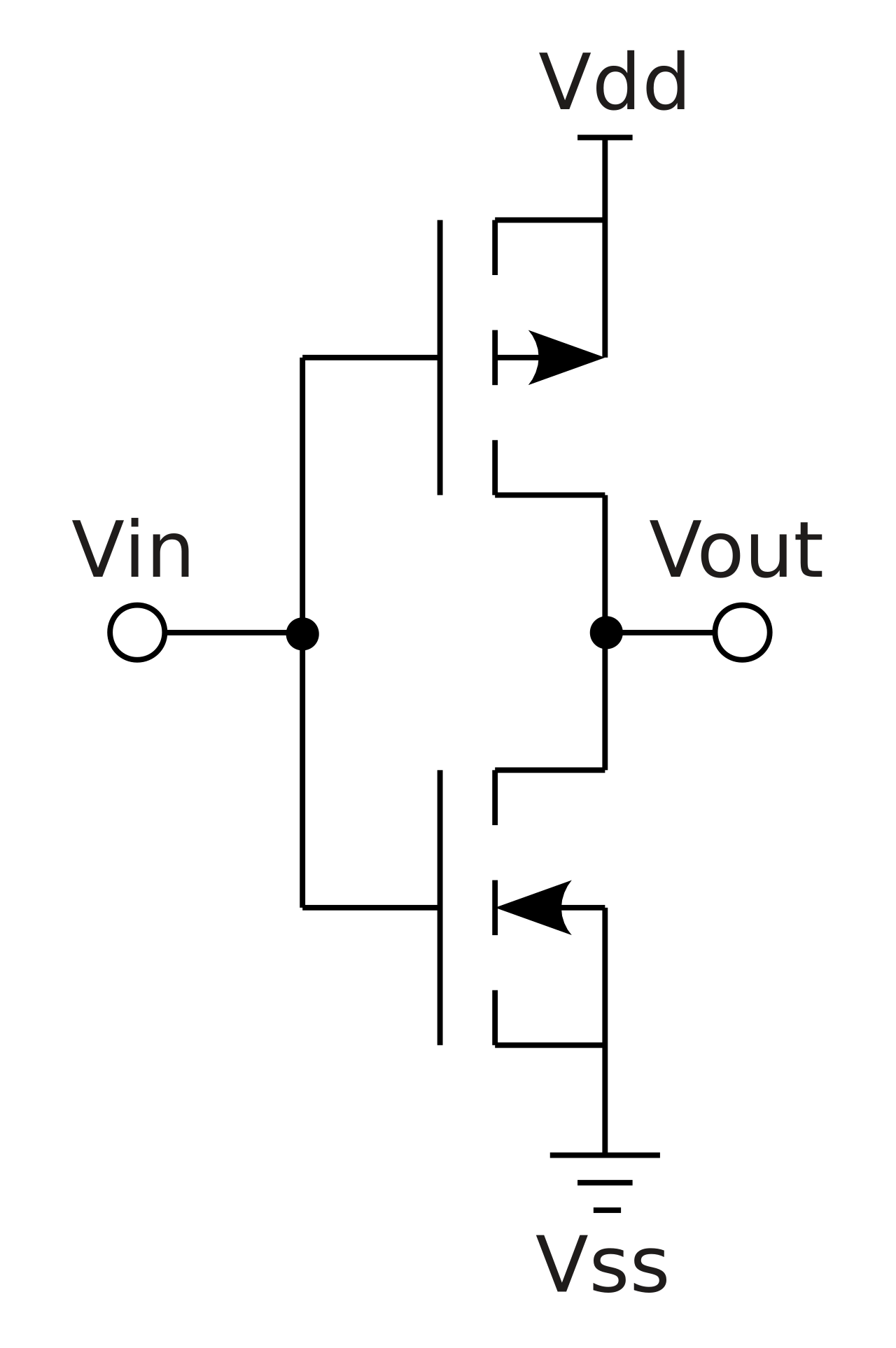
If we feed the gates plus - the n-channel transistor is open, the p-channel is closed. There is no through current, minus at the output. If we feed the gate with a minus - the n-channel transistor is closed, the p-channel is open. There is no through current again, plus output. Those. The element also works as an inverter.
This is the most energy-efficient technology. In a static state, the element consumes nothing (except for the stray leakage current), only the switching current is consumed. Power consumption is almost directly proportional to the frequency of the chip (the number of recharge cycles). Low power consumption and compactness determined the dominance of CMOS technology in digital electronics.
Bipolar transistor circuits initially provided higher performance, but were more complex, took up more space and consumed an order of magnitude more energy. I must say that the choice in favor of CMOS fully paid off. It would be almost impossible to get such characteristics as today's processors on other technologies. And while alternatives are not visible on the horizon.
Topology Features
The chip topology of the chip can be conventionally represented as a large sheet of paper in a cell, where the boundaries of the regions are drawn along the lines, and the technological size is the size of the cell. In fact, for non-critical elements, you can also indent half a cell (the rule of two lambdas), but these are nuances.
Detailed Topology Design
Let us mentally go back to the end of the 1980s, when the technologies were still simple and understandable. Consider a real pair of CMOS transistors. Windows n + and p + are highly doped (1 impurity atom per several hundreds or even tens of silicon atoms), i.e. the level of impurities is orders of magnitude higher than just n and p.
Suppose we were given TK to draw the topology of such a pair of transistors in an isolated pocket. Since there will be no large currents through transistors, we will calculate based on the smallest possible technological size, the so-called technical clearance. Call it d.
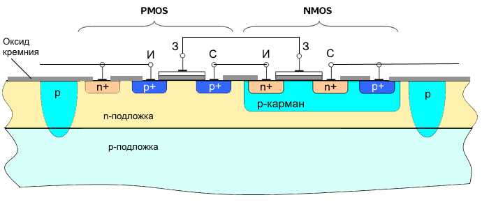
Profile

Top view
We start with the contact window for the source of the n-channel transistor (1) . We make it the smallest possible d * d .
Source (2)then it will have a size of 3d * 3d (you need to step back at least from the edges of the window).
Base (3) is made of the minimum width d .
Further, the stock (4) with its contact window, also 3d * 3d .
The last element is the high-alloy zone (5) for contact with the p-base, and also 3d * 3d . It is needed to equalize the voltage of the source and base, so that the spontaneous appearance of the channel does not occur.
Draw the borders of the p-pocket itself (6) , another d from the drawn windows. The size of the p-window is 5d * 13d .
Below we draw a p-channel transistor. We make this arrangement to approximate the entire element to a square shape - it’s easier to assemble.
We change the location of the source and drain. This arrangement minimizes the length of the contact metal tracks. Let's start with the contact window for the drain (7) , the size is minimal - d * d .
The drain (8) will be 3d * 3d , the base (9) is of width d and in line with the base of the n-channel transistor. The source (10) and the highly alloyed contact area to the base (11) will also be 3d * 3d .
The last size is the minimum offset to the dividing path(12) , more d .
Total received the size of the transistor pair 11d * 15d . The separate track in our case is another p-type region, which with an n-substrate forms a reverse biased pn junction.
There is another option for insulation with a dielectric - silicon dioxide SiO 2 or sapphire Al 2 O 3 . The latter option is preferable, but noticeably more expensive. In this case, the areas can be formed close to the dividing path and the leakage current between the cells will be zero. Typically, the width of the separation track is slightly larger than the thickness of the epitaxial layer (more on this below) and is equal to 2d .
The total effective cell size to the middle of the dividing paths is13d * 17d .
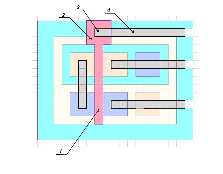
Then, on top of the oxide, draw a shutter (1) , remove the contact area (2) of the shutter closer to the dividing path and form a contact window (3) .
The final stage is metallization and contact paths (4) . Aluminum was originally used as the material of the gate and contact paths (although aluminum is still used in some devices ), later the gate was made of highly alloyed polycrystalline silicon, and the contact paths were made of copper.
Suppose we were given TK to draw the topology of such a pair of transistors in an isolated pocket. Since there will be no large currents through transistors, we will calculate based on the smallest possible technological size, the so-called technical clearance. Call it d.

Profile

Top view
We start with the contact window for the source of the n-channel transistor (1) . We make it the smallest possible d * d .
Source (2)then it will have a size of 3d * 3d (you need to step back at least from the edges of the window).
Base (3) is made of the minimum width d .
Further, the stock (4) with its contact window, also 3d * 3d .
The last element is the high-alloy zone (5) for contact with the p-base, and also 3d * 3d . It is needed to equalize the voltage of the source and base, so that the spontaneous appearance of the channel does not occur.
Draw the borders of the p-pocket itself (6) , another d from the drawn windows. The size of the p-window is 5d * 13d .
Below we draw a p-channel transistor. We make this arrangement to approximate the entire element to a square shape - it’s easier to assemble.
We change the location of the source and drain. This arrangement minimizes the length of the contact metal tracks. Let's start with the contact window for the drain (7) , the size is minimal - d * d .
The drain (8) will be 3d * 3d , the base (9) is of width d and in line with the base of the n-channel transistor. The source (10) and the highly alloyed contact area to the base (11) will also be 3d * 3d .
The last size is the minimum offset to the dividing path(12) , more d .
Total received the size of the transistor pair 11d * 15d . The separate track in our case is another p-type region, which with an n-substrate forms a reverse biased pn junction.
There is another option for insulation with a dielectric - silicon dioxide SiO 2 or sapphire Al 2 O 3 . The latter option is preferable, but noticeably more expensive. In this case, the areas can be formed close to the dividing path and the leakage current between the cells will be zero. Typically, the width of the separation track is slightly larger than the thickness of the epitaxial layer (more on this below) and is equal to 2d .
The total effective cell size to the middle of the dividing paths is13d * 17d .

Then, on top of the oxide, draw a shutter (1) , remove the contact area (2) of the shutter closer to the dividing path and form a contact window (3) .
The final stage is metallization and contact paths (4) . Aluminum was originally used as the material of the gate and contact paths (although aluminum is still used in some devices ), later the gate was made of highly alloyed polycrystalline silicon, and the contact paths were made of copper.
Suppose we live in a 3 micron process technology . Then our two transistor cell 11d * 15d , as shown above, will have a size of 33 * 45 microns . But then we were in trouble, switched to a new process technology of 1.5 microns . The size of our cell became 16.5 * 22.5 microns. And where one cell used to fit, now as many as four fit in. At the same time, these four cells consume current as much as one old one (at the same frequency and current density). Together with the linear dimensions of each transistor, its parasitic capacitance and resistance decreased, and the time of transients during switching decreased. Such a transistor can stably operate at a higher frequency and lower supply voltage. And the consolidation of a larger number of elements on a single crystal minimizes the need to access a slow external bus.

We get that from reducing the size of transistors is one sheer benefit and no harm. That is why miniaturization has become the main task of digital microelectronics since its inception.
What is the technical clearance limited to (it is also the design norm)? To do this, you need to go a little over the technology of manufacturing chips.
Technical processes
Monocrystalline silicon is obtained by the method of slow drawing from the melt ( Czochralski method ). The necessary impurity is added to the melt, which ensures uniform alloying ( note: I would argue with the author of the original, since pure (relatively) silicon is grown according to Czochralski, they are terribly afraid of impurities from the crucible, and they create the required level of alloying only later on the plates themselves, for example, by implantation of ions. Cornelius Agrippa corrects: in fact, impurities can be added directly to the melt when the plates are rusted, so they get plates immediately doped with an impurity (KEF, KDB with different degrees of conductivity) Ion implantation is used later, at the stage of manufacturing chips). At the output, cylindrical boule blanks (boule) with a diameter of 200 or 300 mm are obtained, which are then cut into thin plates ( aka wafers ) with a thickness of about 0.5-0.7 mm. Later, tens and hundreds of microcircuits are formed on them in a single technological cycle. There was an attempt to switch to plates with a diameter of 450 mm, but so far it has not run. It is too difficult to maintain the same process conditions in the center and at the edges of the plate (temperature distribution, impurities, and so on).
Then, on the working side of the plate, a thin layer of silicon with a different type of conductivity is built up - the epitaxial layer. The ways of building are different: for example, by reducing gaseous silicon tetrachloride (SiCl 4) In this case, the dopant is added to the gas. The resulting layer continues the structure of the crystal plate, but has a different type of conductivity. In our example above, we have a p-type silicon substrate and an n-type epitaxial layer. Sometimes pockets of n- or p-type are created on the substrate before epitaxial growth. The so-called hidden layers.
And then comes the process of creating the source, drain, p-base, contact and dividing areas in the epitaxial layer. The essence of technological processes is to remove the oxide in the right places, open the silicon itself, and introduce the necessary impurities into it. Impurities are introduced by diffusion or ion implantation .
During diffusion, a silicon crystal with windows cleaned from oxide is placed in an atmosphere containing a gaseous impurity, and then heated to a temperature above 700 degrees Celsius. Upon heating, silicon atoms begin to oscillate with a larger amplitude, and impurity atoms gradually penetrate into the silicon crystal lattice, as if dissolving. The rate of incorporation exponentially depends on temperature. In principle, the process will also take place at room temperature, but it will only take years to wait. By adjusting the temperature and duration, the desired depth and concentration of the layer are obtained. Heating during subsequent operations can erode already formed layers, therefore, they try to carry out all high-temperature operations at the beginning of the process.
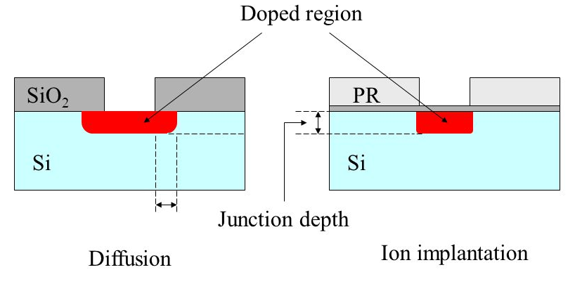
The advantage of the diffusion method is its simplicity and low cost. The downside is that during diffusion, the impurity is introduced not only deep into the crystal, but also along the sides under the oxide. Thus, the actual width of the base is less than that drawn by us. If you overdo it with heating, the source and drain under the gate will close, and the transistor will turn into a resistor. With element sizes of hundreds of nanometers, diffusion is not used.
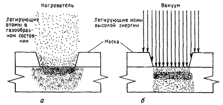
During ion implantation, impurity atoms are ionized, accelerated by an electric field, and a silicon crystal is bombarded. The speed of the ions and the thickness of the oxide are selected so that the ions penetrate into the silicon to the desired depth, but cannot break through the oxide layer. Impurity ions knock silicon atoms out of the crystal lattice or get stuck between the lattice. After implantation, the crystal is heated in order to restore the lattice structure due to thermal vibrations of atoms. The heating temperature is lower than during diffusion; therefore, the impurity entry under the oxide is noticeably less.
And sometimes for special applications it is used where high uniformity of alloying is required, as in power semiconductors, implantation is used in a nuclear reactor . Thanks tnenergy for our
Lithography
And now about the main and most interesting process - lithography. Using it, a layer pattern is created on the surface of silicon. Consider the simplest contact optical lithography (photolithography).
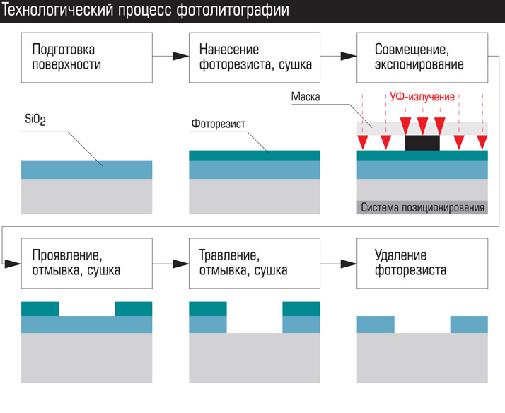
The main steps:
- An oxide film forms on the surface of the silicon wafer.
- A special paste is applied on top of the oxide - photoresist. The plate is untwisted in a centrifuge so that the photoresist spreads uniformly over the surface.
- Combination. From above apply a special mask - a photomask. A layer pattern is applied on it, for example, dividing tracks or p-pockets of all elements of all microcircuits on the plate. The photomask under a powerful microscope is combined with the plate using alignment figures ( note: special cross marks) and high-precision mechanics.
- Exposure. The plate is irradiated with ultraviolet light through a photomask. Under the influence of radiation, the photoresist changes its properties, softens (in the case of a positive photoresist) or tanning (negative photoresist). Next, we will consider the case with a positive photoresist.
- Manifestation - the irradiated photoresist is washed off with a solvent and an oxide layer underneath opens.
- Oxide Etching. In unprotected photoresist areas, oxide is removed by hydrofluoric acid or a beam of ionized inert gas. Hydrofluoric acid is cheaper, but it dissolves not only exposed areas, but also slightly undermines the oxide under the photoresist (the same shadowing effect).
- Complete removal of photoresist with a more vigorous developer.
At the end of the operation, we obtain a plate with the removed sections of oxide, which can be sent for diffusion, ion implantation or metal deposition ( note: or electrodeposition). After creating the layer, the oxide is usually etched from the entire area of the plate and a new one is deposited.
Windows create from wide to narrow. In our case, the sequence will be as follows: separation areas, p-pockets, p + layers, n + layers, contact windows with metallization, application of the shutter, contact areas of the shutter, the first layer of metal tracks with contact areas under the second layer, the second layer of metallization, etc. . In modern processors, metallization is up to 10-15 layers.
Contact photolithography was used at the dawn of microelectronics. Now the main thing is projection photolithography. This is when a lens and mirror systems are placed between the radiation source and the photomask to create a narrowing beam of photons. Schematically different methods of photolithography are shown in the figure below: contact photolithography, with a gap, projection through lenses, projection mirror.

The advantages of photolithography are high speed and low cost. The entire plate area with all its microcircuits is exposed at once, and the process takes several minutes. Or a square of several microcircuits followed by a plate shift.
In addition to photolithography, there are other types - electronic, x-ray and ionic. The most interesting is electronic lithography (for example, the Mapper project, about which he wroteBarsMonster ).
With electronic lithography, the exposure of the resist is carried out not by light, but by a beam of electrons. In its simplest form, it resembles image formation on CRT picture tubes . Of all types of lithography, it is electronic lithography that provides the clearest picture and highest resolution. The disadvantage is the long exposure time. In modern technologies, the electron beam has a thickness of a few nanometers and even fractions of a nanometer, and the plate diameter is 300 mm. Naturally, not one bundle is used, but tens of thousands controlled by a computer. But a very powerful total electron flux is required. For comparison, the energy of the UV radiation quantum is several eV , the electron energy in the beam is several thousand electron volts.
In addition, the electrons are electrically charged and repel each other, which leads to a beam divergence. Of course, it is possible to increase the speed of electrons, but then they will pierce the resist through or reflect at a high speed in arbitrary directions, causing secondary radiation ( Secondary Electrons ) and, accordingly, exposure. All this limits the use of technology.
Electronic lithography is used to create photomasks. Exposure time for one photomask is several days. Therefore, photolithography dominates in the production of microcircuits.
A modern set of photo masks for a processor costs tens of millions of dollars. Not surprisingly, given that modern processors contain billions of transistors, and there are hundreds of processors on the plate. In addition, the windows in the modern photomask are not just holes in the material, but often other materials with specific optical properties. A real set of photo masks consists of dozens of masks. At the latest manufacturing processes, more than 50 ( sic! ).
But they allow you to stamp microchips like hot cakes. During its lifetime, a set of photo templates allows you to get hundreds of thousands or even millions of microchips at the output.
So what limits the size of the process technology?
4 groups of factors can be distinguished conditionally:
- Hardware and technology. Associated with hardware resolution.
- Physics of technological processes. It is determined by the physical limitations of a particular process, which can be circumvented by a change in technology or materials.
- Physical. These are limitations that cannot be circumvented, but their impact can be minimized.
- Extreme physical.
Hardware and Technology Limitations
This type of limitation was decisive in the early stages of microelectronics. Mainly refers to the production of "clean rooms", sophisticated equipment for technical processes, instrumentation (which is important for quality control of products). For example, photolithography requires ultra-precise optics, powerful microscopes, mechanisms for combining masks and plates with an accuracy of fractions of nanometers, an ultrapure atmosphere or vacuum during exposure, and so on. It is necessary to very accurately withstand the parameters of technological processes - temperature, duration, atmosphere composition, radiation power, surface preparation.
Now the accuracy of the equipment is not a limiting factor. Not because it is a simple problem. It is enough to look at a diagram of a modern projection or mirror photolithography to understand the level of complexity. But here is really the case when there are no barriers for talented designers and engineers.
Problems with technology are usually relevant in the first series. With a change in the technical process norm, not only the horizontal, but also the vertical dimensions, and the concentration of impurities, and the proportions of the active zones change. And now, with each new step, the physics of processes is also changing. Naturally, all parameters are preliminarily calculated and modeled, but reality always makes adjustments. Therefore, for the first series, 3% yield of suitable circuits (97% defective) is considered the norm. Gradually, technological processes are optimized and the percentage of yield suitable for the last series becomes over 90%.
Physics of technological processes
For more than 30 years, until recently, it was these factors that were limiting. I have already listed some of these limitations — the entry of impurities under the oxide during diffusion, gnawing of the oxide under the photoresist during etching, and the erosion of already deposited layers during thermal processes.
Solution methods are also partially described.
Diffusion was replaced by ion implantation. Plus, for the smallest layers, the impurity material was changed - instead of phosphorus, arsenic is used, instead of gallium boron. Their atoms are larger and heavier, therefore they dissolve worse in silicon at the same temperatures (and most importantly, it is more difficult for them to diffuse!). For ion implantation, this is not important, but upon subsequent heating, such layers erode much more weakly.
The production of oxide by heating has replaced the low temperature catalytic deposition from gas. Heating is used, but only at the very beginning, while the crystal is clean. In some operations, silicon nitride (Si 3 N 4 ) or successive layers of oxide and nitride are used instead of oxide .
Liquid acid etching was changed to ion etching. Acid is used only to remove oxide from the entire area.
Another problem was the production of ultrapure oxide for a gate dielectric. This oxide remains as a working element on the chip, and has high requirements for purity and uniformity. The oxide thickness in places is less than 10 atomic layers. A small defect leads to a puncture or breakdown. This gives an electric closure of the shutter to the base and the failure of the element. For some time, an alternation of a layer of oxide and silicon nitride was used. In 90 nm technology, hafnium oxide HfO 2 was used as a gate dielectric .
By the way, during the USSR it was precisely the problems with obtaining high-quality oxide that slowed down the transition to CMOS. Hence the search for alternative paths and the general lag in digital microelectronics.
The most critical operation is photolithography. So much so that so far many have put an equal sign between the resolution of the entire technical process and the resolution of photolithography. And the main problem of photolithography since the late 1980s is the diffraction of light. More precisely, ultraviolet radiation, although the principle is the same. It would not be an exaggeration to say that for 30 years the struggle to reduce the size of technological processes was primarily a struggle against diffraction.
The diffraction of light was discovered back in the 18th century by the fathers of the founders of optics:

When penetrating into the hole, the rays of light and any other electromagnetic radiation (EMP) deviate from the straight path, diverge and penetrate into the shadow area. The phenomenon is observed at hole sizes close to the wavelength. The smaller the hole compared to the wave, the stronger the dispersion. The rule is valid up to quarter-wavelength gaps. The hole is less than a quarter of the wavelength, the EMP beam simply “does not see” and is reflected from the surface with such small gaps as from a solid one.
The wavelength of silicon LEDs is about 1 μm (near infrared), the wavelength of visible light from 780 nm (red) to 380 nm (purple). Less than 380 nm, ultraviolet radiation (UV) begins. The emitters used today in photolithography have a wavelength of 248 nm and 193 nm, this is the radiation of excimer lasers (for example,on XeF 2 ). Accordingly, diffraction problems rose to their full height after overcoming the 3 micron technology bar, and after 800 nm they became dominant. Due to diffraction during exposure, the UVI enters the area under an opaque mask and illuminates the photoresist in the shadow. As a result, instead of a clear square, we get a blurry pancake.
In addition to erosion of windows, there is the effect of overlapping (interference) side waves for closely spaced windows. Flare peaks appear far below the reflective part of the photomask.
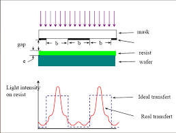
Optics - heartless you ...
What methods are used to combat this phenomenon?
The first step was to use projection photolithography. If greatly simplified, a lens is installed between the photomask and the plate, which collects diverging rays and focuses them on the photoresist.

Another method was to reduce the wavelength of the exposure radiation. At one time, they started with arc mercury lamps with a radiation wavelength of 436 nm - this is blue light. Then 405 nm (violet), 365 nm (near ultraviolet). On this, the era of mercury lamps ended, the use of excimer lasers began. First, 248 nm (medium ultraviolet), then 193 nm (deep ultraviolet). On this process and stalled.
The fact is that they reached the transmission limits of quartz optics. Shorter waves absorb quartz. It was necessary either to switch to mirror systems, or to use lenses from other materials. Experimental installations at 157 nm were made based on calcium fluoride optics. However, they never went into the series. Since there were ways to optimize 193 nm lithography.

Visual infographics on lasers. A source
EUV lithography
In the mid-1990s, they developed a standard photolithography on extreme ultraviolet ( EUV lithography ) with a wavelength of 13.5 nm. This wavelength made it possible to give a resolution in units of nm.
By the early 2000s, the first experimental samples appeared.
By the end of the 2000s, technology was supposed to go into a series. And finally, the news came that in 2019 Samsung and Taiwanese TSMC will switch to EUV lithography. Less than 15 years have passed ( sic! ). Intel became the main antagonist of EUV lithography, although it was originally one of the initiators. Recognizing that everything that was possible was squeezed out of the 193 nm UVI, they announced the transition to 126 nm (ha ha!).
What is the reason for this rejection?
The fact is that 13.5 nm is already practically x-ray radiation. The boundary between UVI and X-ray is conventionally considered 10 nm, but ultraviolet is no different from soft X-ray in the behavior of 13.5 nm. Therefore, EUV lithography is more like x-ray. Lenses for such a wavelength do not exist in nature, therefore, it is necessary to switch to mirrors from heterogeneous layers of metal.
In addition to producing a very thin and complex structure, metal mirrors absorb most of the radiation. Units of percent of the initial radiation power reach the photoresist. If we take into account that the efficiency of the emitter itself is also a few percent, then to obtain a normal exposure time, high power and high energy consumption are needed ( ooops! ).
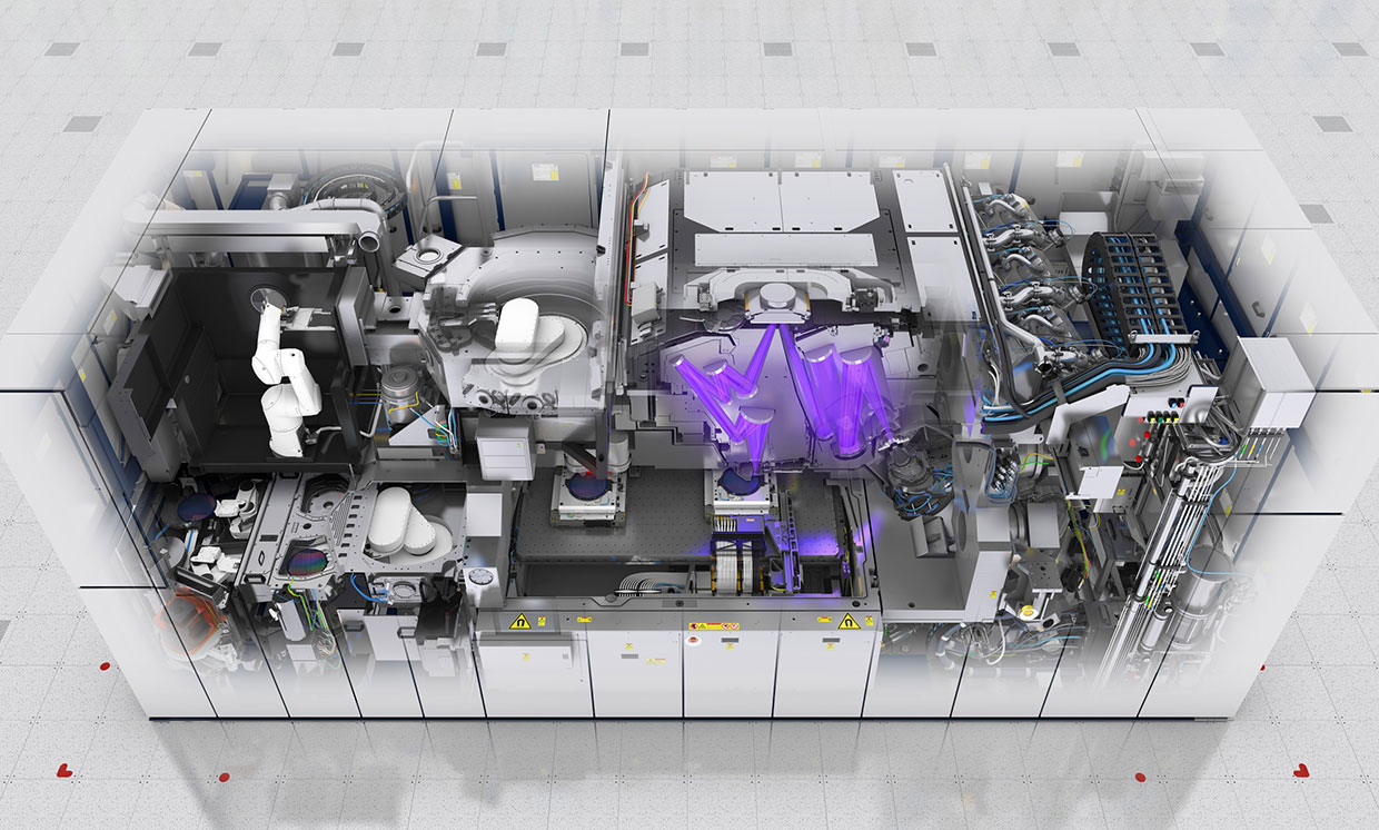
This is how ASML's EUV scanner looks. The
source of radiation is plasma. A very capricious substance, from which it is difficult to achieve a uniform flow without pulsations. Even air actively absorbs 13.5 nm, so exposure can only be carried out in vacuum.
The problem with the selection of photoresist. The shorter the wavelength, the higher the photon energy. Previous sources gave energy in units of electron volts, this is the usual energy of chemical reactions. The photon energy for a wave of 13.5 nm is 92 electron volts. This is the binding energy of deep electrons. Absorbing such a photon, the electron becomes very "hot", begins to rush, radiates excess energy and causes secondary exposure away from the window. Therefore, the selection of a photoresist with the desired set of parameters is also a difficult task.
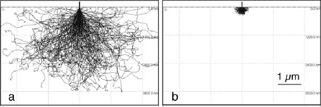
Monte Carlo simulation results of electron travel in silicon with energies of 20 and 5 eV. Source
These difficulties determined the reasons why they postponed the transition to EUV to the last.
Actual methods of combating diffraction
So, until recently, the same UVI with a wavelength of 193 nm was used as a radiation source. Up to the technology of 10 nm and 7 nm. And now we recall that radiation cannot penetrate the gap if its width is less than a quarter of the wavelength. For 193 nm it is 48 nm. The question arises - HOW ?!
This is the little miracle that the engineers did. They used the radiation polarization method.
We take a rectangular narrow gap (with a width of less than a quarter of the wavelength) and direct light toward it, polarized along the axis. Light will pass through the gap; even diffraction in the transverse direction will be negligible.
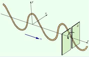
And now we take 2 perpendicular slots: horizontal and vertical. First, we irradiate a two-component photoresist with polarized light through a vertical slit, and then through a horizontal one. Only the area irradiated 2 times appears. Just like all ingenious.
True, you will have to use 2 times more photo templates and 2 exposure processes to create one window. But you can use the good old quartz optics and proven photoresists for years. What a twist!
There are other ways to combat diffraction ...
Optical proximity correction. The shape of the windows of the photomask is made non-rectangular to compensate for defects during diffraction.
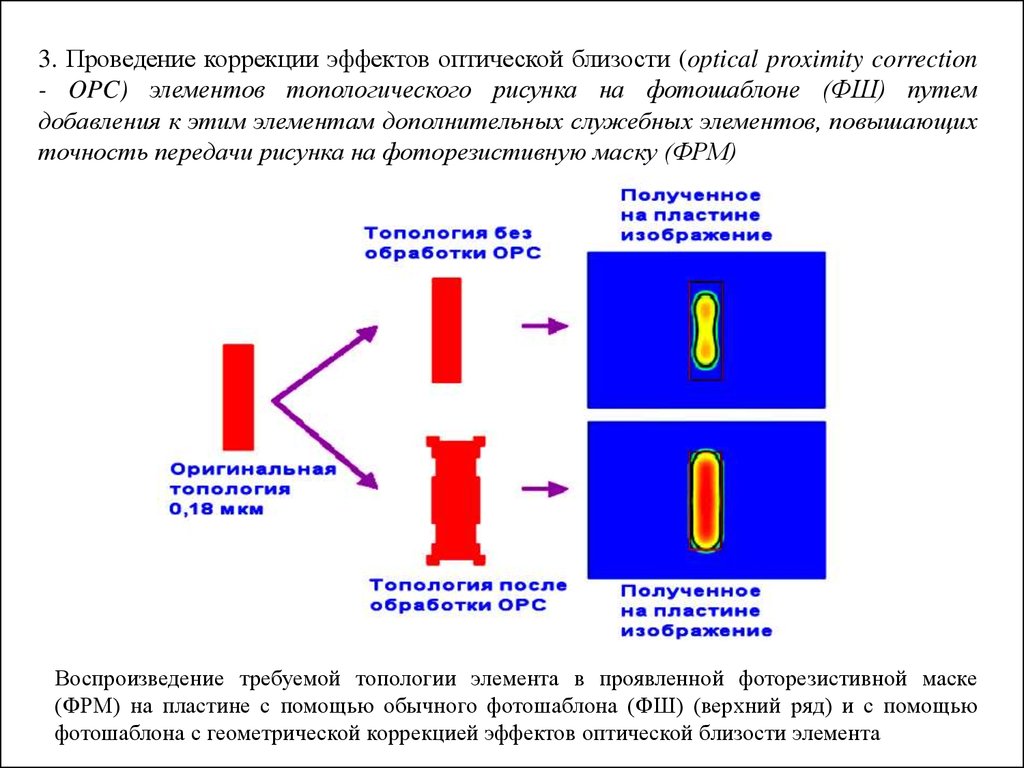
The method of correcting optical proximity is schematic ...
Using phase-shifting masks. On the sides of the main window of the photomask do auxiliary, the material of which shifts the phase of the wave. When waves are applied ( interference ), they partially cut off lateral displacements from each other.
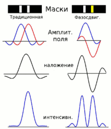
Off-axis lighting. The beam does not fall perpendicular to the surface of the plate, but from two sources at a slight angle. When applying sources, lateral displacements are partially compensated.
Multiple exposure.For example, we need to make exposure of six nearby windows. First we drive the exposure of 1, 3 and 5 windows. And then 2, 4 and 6. This increases the number of exposure cycles and photo templates by 2 times, but still better than nothing. Given the horizontal and vertical polarization, we get 4 exposure cycles to create one layer.
Thus, if we look at the modern photomask, then we won’t see the areas of the microcircuit in explicit form. There will be a set of horizontal and vertical figures, which, when superimposed, will give a picture. Actually, solid Chinese characters: maybe that is why the Chinese occupied the production of microelectronics ?!
After 45 nm, they switched to immersion photolithography. This is when the space between the extreme lens and the photoresist is filled with liquid. At first it was water. Now special fluids with a high refractive index (up to 1.8). The liquid reduces the effective wavelength and neutralizes the refraction of light at the interface of the media.
This is how they reached the resolution of ~ 10 nm. But this seems to be the limit for 193 nm lithography.

Photo of the first metallization layer for 24 nm technology. On the left, created by 193 nm lithography, on the right experimental 13.5 nm (EUV). As you can see, from the previous clear rectangular shapes there are only memories. Still works.
About physical limitations, how they affect and how they changed production in the second part in a couple of days - stay tuned!
Do not forget to subscribe to the blog : it’s not difficult for you - I am pleased!
And yes, please write about the shortcomings noted in the text in the PM.
