Popular misconceptions about the radiation resistance of microcircuits
In about every second topic on Habré relating to astronautics or electronics, the topic of radiation resistance pops up. The topic of import substitution of a radiant-resistant element base runs through the news about domestic space exploration, but at the same time, Elon Musk uses cheap conventional chips and is proud of it. And the Israelis in Bereshit used a radiant processor and are also proud of it. And in principle, the microelectronic industry in Russia lives largely due to a state order with the relevant requirements. Observing regular disputes about how to properly build satellites shows that the training of participants is usually low, and their argumentation is burdened with stereotypes that were accidentally heard out of context facts and knowledge that were outdated many years ago. I thought that reading this is no longer strength, therefore,
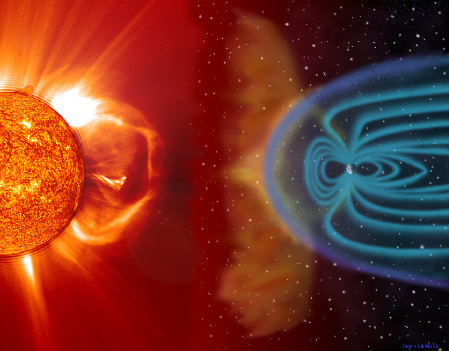
Figure 1. An indispensable beautiful picture about cosmic radiation and the fragile Earth.
The most popular theses on radiation resistance used in near-space disputes look something like this:
As you can see, some of these theses directly contradict each other - which is regularly the subject of controversy or the reason for far-reaching incorrect conclusions.
You need to start the conversation with an important disclaimer: radiation resistance is not the center of the world and the only quality that should be suitable for use in space or other aggressive environments chip. Radiation resistance is only one requirement from a long series, which includes reliability, extended temperature range, resistance to electrostatic discharge, vibration resistance - and reliable confirmation of all of the above parameters, that is, long and expensive certification. It is important everything that may not allow the chip to work out the entire required service life, and most applications of radiant-resistant chips imply the impossibility of repair or replacement. On the other hand, if something is wrong with one of the parameters, the designer of the final product can often find a way around the limitation - to place the chip that is most sensitive to the dose of radiation behind a thick wall, monitor the current consumption of the chip that is vulnerable to the thyristor effect and reset its power if necessary, or thermostat the chip with a narrow temperature range. Or it may not be found, and the only way to solve the task will be to order a new ASIC radar resistant.
It is also useful to remember that developers of special-purpose systems are the same people as any other developers. Many of them also like to write code for crust-filled crutches to yesterday’s deadline and use more powerful hardware so that it definitely works on it; some would have used Arduino if it had been properly certified. And, of course, people who set tasks for developers of special-purpose systems and developers of microcircuits for them rarely feel shy in the requirements for reliability, performance, and joy resistance. Therefore, modern design standards on satellites are still needed - I want large amounts of DRAM, multi-core processors, and the latest FPGAs. I already mentioned above thatnothing lack of data on what exactly needs to be circumvented than the commercial status of the chips.
The concepts of “radiation resistance” and “radiation-resistant microcircuit” are grand simplifications. In fact, there are many different sources of ionizing radiation, and they can affect the functioning of electronic devices in different ways. Accordingly, for different applications, resistance to different sets of influencing factors and different levels of exposure is necessary, so a “stable” microcircuit designed to operate in low Earth orbit is absolutely not required to work normally when analyzing blockages in Chernobyl.
Ionizing radiation is called ionizing, because the release of energy in the volume of a substance during braking of incoming particles ionizes the substance. Each material has its own energy necessary for ionization and creation of an electron-hole pair. For silicon, this is 3.6 eV, for its oxide - 17 eV, for gallium arsenide - 4.8 eV. Also, an incoming particle may not ionize an atom, but “move” it from the right place in the crystal lattice (in silicon, this requires 21 eV to be transferred to the atom). The electron-hole pairs created in a substance can have different effects on the electrical and physical properties and on the behavior of the electrical circuit. Radiation effects can be divided into four large groups: effects of the total absorbed dose, effects of dose rate, effects caused by the ingress of single particles, and effects of displacement.
Dose effects
The total absorbed dose of radiation is measured in rad, indicating the substance that absorbs radiation. 1 rad = 0.01 J / kg, that is, the amount of energy released in a unit mass of a substance. Less commonly used is a unit of measure of Gray, equal to 100 rad (or 1 J / kg). It is important to understand that the absorbed dose in different substances will vary for the same number of ionizing particles released by the radiation source (this is the exposure dose). In the case of silicon microcircuits, the desired material is silicon oxide, because the effect on it, and not on silicon, mainly affects the electrical characteristics of the circuit, since the mobility of holes in SiO2 at normal temperature is so small that they accumulate in the oxide, creating built-in positive charge. Typical dose resistance levels of commercial microcircuits lie in the range of 5-100 krad (Si), radiation resistance levels demanded by customers start at 30 krad (Si) and end somewhere around 1 Grad (Si), depending on the purpose of the microcircuit. The lethal dose for humans is about 6 gray.
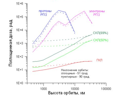
Figure 2. Examples of calculations of the set of the total absorbed dose over 10 years in various circular orbits for protection of 1 g / cm ^ 2. Source - N.V. Kuznetsov, “Radiation hazard in near-Earth orbits and interplanetary trajectories of spacecraft”.
The effects of the full dose are associated with the accumulation of this positive charge in dielectrics and are manifested in CMOS schemes in several main ways:
In bipolar schemes, the main dose effect is a drop in the gain caused by an increase in the base current due to leakage from the emitter to the base at the interface of silicon and passivating oxide. Another dose-specific effect for bipolar transistors is that they can (not necessarily) respond not only to the level of the dose accumulated, but also to the speed of its collection - the slower the dose is accumulated, the worse the resistance. This effect is called ELDRS (Enhanced Low Dose Rate Sensitivity) and it greatly complicates and increases the cost of testing, often not only bipolar, but also CMOS circuits - because they also sometimes have bipolar transistors and because it is easier to get everyone to test uniformly than figure out where ELDRS may be and where not.
Dose rate
Another part of the effects related to the dose rate is an ultrafast dose set at which so many electron-hole pairs are generated in the microcircuit that they do not have time to recombine, and a huge electric charge is introduced into the chip, which dissolves through the ground and power lines during significant time - for which the circuit stops working. This time is called the “loss of working time” and is the main characteristic of the resistance of a microcircuit or device to such effects. In addition, a large amount of the charge introduced into the microcircuit seriously changes the potentials of the areas connected to the ground and to the power supply - which can lead to the appearance of a thyristor effect.
It is the effects of a high dose rate — for the sake of resistance to which the technology “silicon on sapphire” and “silicon on an insulator” was originally developed, because the only way to reduce the charge introduced into the circuit is to separate the active region of the microcircuit from the volume of the substrate, not giving the charge from the substrate to participate in the process. Why are these effects important? A high dose rate over a short time is a typical consequence of a nuclear explosion.
Single effects
Single effects are not associated with prolonged exposure to radiation, but with the measurable effect of a single ionizing particle. They can be divided into two large groups:
The specific energy yield of the ionizing particle is called “linear energy transfer” (LET) and is measured in MeV, transferred per unit length of the particle’s span in the material, per unit density of the material, that is, in (MeV * cm ^ 3) / (mg * cm) or (MeV * cm ^ 2) / mg. The LET is nonlinearly and nonmonotonically dependent on the particle energy and is interconnected with the mean free path, which for particles and materials relevant in microelectronics can range from hundreds of nanometers to hundreds of millimeters.
The number of particles found in space decreases with the growth of LET (see Figure 4). Important values are 30 (corresponds to iron ions) and 60 or 80 (after which the probability of the event is considered negligible). In addition, an important figure is 15 MeV * cm ^ 2 / (mg) - this is the maximum LET that the products of a nuclear reaction may have when a proton or neutron enters silicon. Protons are one of the main types of solar radiation, and although their own LET is small (tenths of a unit), they have a significant effect due to nuclear reactions and secondary ionization. Secondary ionization can occur directly in the active region, or it can be the result of a proton entering an atom of some material with a large atomic number - for example, tungsten or tantalum. Heavy elements are actively used in modern microelectronic technology, for example, to create contacts from silicon to the first metallization layer. Secondary ionization is also the reason why it is not necessary to pack chips in lead boxes to increase radiation resistance.
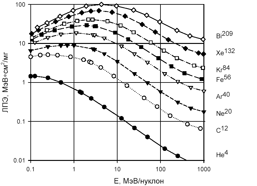
Figure 3. The dependence of LET on energy for different types of particles.
Separately, it is worth paying attention to helium nuclei (alpha particles) - not only because there are a lot of them in the composition of solar radiation, but also because quite a lot of sources of alpha radiation can be found in ordinary life.
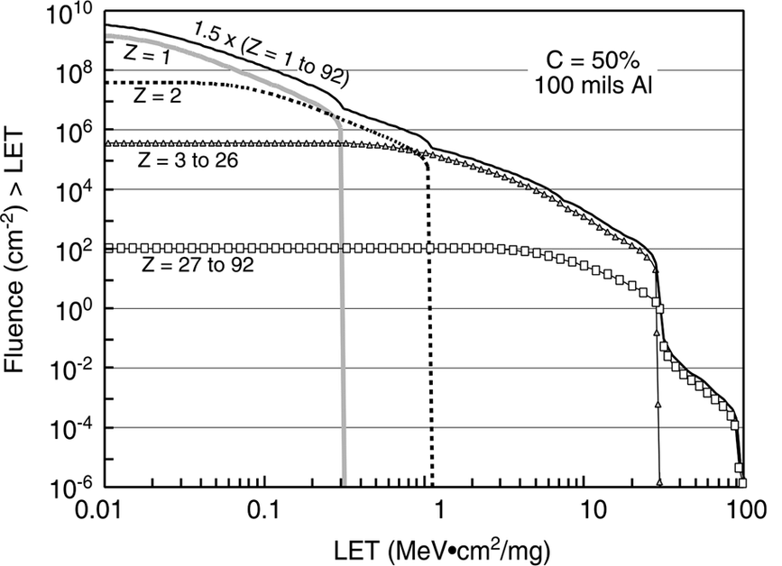
Figure 4. Comparison of the number of particles of different types over a two-year mission in orbit, according to Xapsos et.al., “Model for Cumulative Solar Heavy Ion Energy and Linear Energy Transfer Spectra”, IEEE TNS, Vol. 5, No. 6., 2007
1, 30 or 60 MeV * cm ^ 2 / (mg) - how much is this? The failure threshold of a standard memory cell in 7 nm technology is much lower than unity, in 180 nm - in the range from unity to tens. The use of special circuitry allows you to raise the threshold, for example, to hundreds, but it is usually more reasonable to achieve a figure of 15 or 30 units, and filter out the remnants of rare events using noise-resistant coding. 60 units is a figure that usually appears in the requirements for resistance to destructive effects.
Displacement effects
Displacement effects are local destruction of the crystal lattice, that is, “knocking out” of an atom from its intended place. The energy required to damage the crystal lattice is usually quite large, so most passing particles do not cause this effect. But its cause may be a nuclear reaction as a result of the hit of a proton or neutron, which are many in orbit. Such local lattice defects lead to a decrease in the mobility of charge carriers, an increase in noise, and some other effects. They affect conventional CMOS chips less than “ordinary” dose effects, but dominate in solar panels, photodetectors, power transistors, as well as in complex semiconductors that do not have oxide, for example, gallium arsenide and gallium nitride. This explains their high dose resistance - they simply do not have effects that cause rapid degradation of silicon chips, and what is there is weaker and later. The amount of radiation causing bias effects is measured in particles (usually protons or neutrons) per square centimeter of chip area.
So, with a description of the influencing factors of radiation figured out, now let's see where and in what combinations they threaten microcircuits.
Figure 2 shows an example of calculating the full dose set in different orbits. Next, we need to discuss a lot of assumptions - solar activity, shape, material and thickness of protection, and so on, but in general, despite the fact that the picture is a typical spherical horse in a vacuum, the trend is clear: in different orbits, the speed of the full dose can vary by five orders of magnitude. At the same time, in low orbits, under the first belt of Van Allen, the dose is accumulated so slowly that many ordinary commercial microcircuits can withstand several years in such conditions. Yes, that microchips, even much more fragile people fly there for years without serious health consequences. Meanwhile, low orbits are almost the entire manned space program, remote sensing of the earth, satellite communications, satellite Internet promised very soon and,
Commercial microcircuits in low orbits
Actually, it is precisely because of the popularity and importance of low orbits that the legs of speculation about the fact that expensive radiant-resistant microcircuits are not needed grow, and it is quite possible to dispense with ordinary ones. But the use in space of commercial microcircuits also has pitfalls, which appear even in low orbits.
First, van Allen belts protect the Earth and its immediate surroundings only from light particles, mainly from solar electrons and protons. Heavier particles, although they are much less common, calmly fly even to our last shield - the atmosphere - and, correctly, cause single effects, including the thyristor effect, which can at any time irreversibly destroy any chip and with it the entire spacecraft . Therefore, commercial microcircuits can only be used if measures are taken to protect them from single effects.
The second problem is that the chips on the satellite are not only processors and memory, but also many other types of chips, including power and analog ones, and with their radiation resistance everything is much more complicated and much less predictable. And modern systems on a chip contain a large number of non-digital blocks; for example, for most flash memory chips, the high-voltage generator used for recording is the first to stop working, and for analog CMOS circuits, the reference voltage generated by a pair of bipolar transistors shifts, and even small leaks can seriously change the operating point of low-power analog cascades. The resistance of power keys to destructive single effects can greatly depend on the voltage applied to them, and so on and so forth.
The third important problem of using commercial microcircuits in space is that resistance to the full dose and thyristor effect is sensitive to changes in the process parameters, including small ones, so if something is changed at the factory, you can throw the results of your tests into the trash . And for commercial microcircuits, the manufacturer guarantees the stability of functional parameters, not the technological process. Moreover, in different batches you may encounter crystals from different factories; for example, the processor from the sixth iPhone, Apple A9, was made on 16 nm TSMC and 14 nm Samsung, and the user was not informed which version is on his phone. Trusted Foundry institutes or certified technical processes are used to combat this problem all over the world for the development of rain-resistant microcircuits - in short,
In total, the correct answer to the question “is it possible to use conventional commercial microcircuits in space?” Is: “Yes, it can, in some orbits and subject to a number of requirements and conditions.” Useful advice: if you still decide to use a commercial chip and invest in its testing, buy a stock immediately ten years ahead. Incidentally, this is quite a business model for a large and respected company 3DPlus - they test all commercial microchips in a row for joy, find those that have (essentially random) sufficient performance, purchase large quantities and then pack the chips in their own enclosures under their own brand .
Other orbits
However, satellites fly not only in low Earth orbit. As an example of other requirements, let's look at the only way to ensure stable communication in the vicinity of the North Pole - and this is a strategically important area for Russia - the Molniya orbit, named after the first spacecraft launched on it.
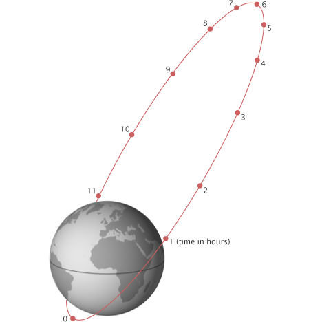
Figure 5. Orbit “Lightning”.
The main feature of this orbit is that due to its great elongation (the minimum height is about 500 km above the Earth’s surface, the maximum is up to 40,000 km, the period is 12 hours), the apparatus crosses radiation belts four times a day. The active life of the very first Molniya satellites was only about six months, primarily because of the radiation-induced drop in the power of the solar panels, which needed to power a powerful (high orbit) radio transmitter.
In geostationary orbits of navigational aids, Figure 2 promises us a dose of several hundred crad (Si) - and the dose resistance of commercial microcircuits can easily be 5-10 crad (Si), that is, about 10-15 years of active existence of such chips there can be no speech in orbit. More precisely, it can, but for this you will need a much thicker protection - or protection from something more dense than aluminum. However, here we plunge into the marvelous world of spacecraft design, so let's limit ourselves to the phrase that delivering every kilogram to orbit is expensive, and the idea of hiding the most vulnerable electronics deeper inside the case, shielding it with other components is not bad, but completely problematic won't decide.
Military chips
When dealing with the issue of debunking myths about joy resistance, it is imperative to say that you cannot equate “joy-resistant”, “space” and “military” microcircuits. Not all military microcircuits are radio-resistant, and not all radio-resistant microcircuits are military. If we turn to the American military standard Mil-Std-883 (to the American, because its Russian counterpart is classified in terms of radiation), then we will find in it many different tests for the influence of the environment - thermal cycling, humidity, air with sea salt, etc. .d. etc.
Radiations concern the following points:
1017.2 Neutron irradiation
1019.8 Ionizing radiation (total dose) test procedure
1020.1 Dose rate induced latchup test procedure
1021.3 Dose rate upset testing of digital microcircuits
1023.3 Dose rate response of linear microcircuits
Complete dose and dose rate. Single effects? No way. The technical specifications for the microcircuit may include requirements for resistance to single failures and / or thyristor effect, but these requirements are not standardized and are determined again each time, based on the needs of specific customers of each chip. It turns out that the status of "military" is not a guarantee of the ability to launch the chip into space? Yes it is. An example is the fate of the infamous “Phobos-soil”, the death of which was caused, according to the official version (very difficult to prove, but very convenient), by the hit of a heavy charged particle in the American military-class memory chip, which was not resistant to single failures .
Peace atom and others
The importance of radiation resistance is not limited to space and military applications. The natural background radiation at sea level is many times lower than even what happens in low orbit, but the Earth’s atmosphere not only serves as the last shield on the path of cosmic radiation, but also gives rise to secondary particles when interacting with it. Secondary particles are mostly neutrons. Appearing in the upper layers of the atmosphere, they usually do not reach the surface, however, at the altitudes of civilian airliners, the radiation dose is also significant and very impressive statistics are collected for single failures. X-rays are used in medicine a long time ago, and radiotherapy is one of the important ways to fight malignant tumors, and such devices also need electronics.
And, of course, do not forget that all the fuss with the lead-free solder dearly beloved by all electronic engineers was started largely due to the fact that lead and some other materials used in the manufacture of microcircuits contain impurities of heavier elements, in particular uranium, and their application leads to the generation of a small, but still well-measurable alpha particle flux - right next to vulnerable silicon. In the case of BGA-cases or 3D-assemblies - over the entire surface of vulnerable silicon.
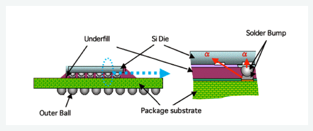
Figure 6. Illustration of a solder ball as a source of alpha particles.
The good news is that alpha particles have a rather small mean free path in silicon (from units to tens of microns, depending on energy), and multilayer metallization helps to reduce their effect. The bad news is that at low design standards, all alpha particles that still reach silicon, cause failures, not only single, but also multiple (more on this below). For example, last year TSMC published an article at the 2018 IEEE International Reliability Physics Symposium on measuring the number of failures from pollution by alpha particles in memory according to design standards of 7 nm, that is, this problem continues to exist and requires some action in a world where everything switched to lead-free solder.
Another application of radiation-resistant circuits, which I would like to say a few words about, is high-energy physics and atomic energy. In the active zones of hadron colliders and nuclear reactors (as well as in equipment designed to eliminate radiation accidents), electronics are also needed, and it is highly desirable that one that does not need to be replaced and repaired for a considerable time. The requirements for the total absorbed dose for such applications are tens and even hundreds of Megarads (Si), that is, three orders of magnitude more than in conventional space applications. To complicate the situation, such resistance is required not from digital circuits, but from power and analog ones - electric drive control circuits and primary processing of multichannel sensors readings.
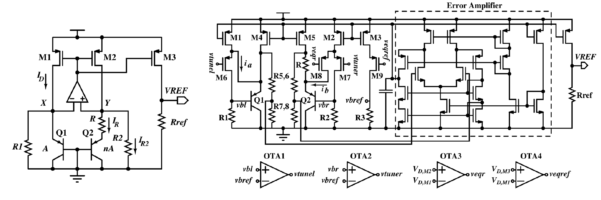
Figure 7. Normal and joy resistant reference voltage circuit. From Y. Cao et.al., “A 4.5 MGy TID-Tolerant CMOS Bandgap Reference Circuit Using a Dynamic Base Leakage Compensation Technique”, IEEE TNS, Vol.60, N.4, 2013
I will illustrate the scale of the challenges facing developers of chips for nuclear energy with my favorite example. A reference voltage source (ION) equal to the band gap of a silicon bandgap voltage reference is a relatively simple and well-known circuit. Under the influence of radiation, the parameters of bipolar transistors used as diodes change (the gain decreases due to the appearance of an emitter-base leak). As a result, the reference voltage of a conventional ION circuit, which determines the accuracy of all measurements, can shift, say, by 15–20%, which corresponds to an effective ADC resolution of two to three bits. In the circuit on the right, the reference voltage varies within 1% (which is more than 7 bits) at a dose of ionizing radiation of 4.5 MGy. In order to achieve this impressive result, the scheme had to be seriously reworked, adding a whole bunch of feedbacks to compensate for dose leakage. In the rainproof version, there are approximately four times more elements than in the normal version, and its energy consumption is twice as much. And the worst news is that for each new scheme, the radiation resistance strategy and its implementation have to be developed separately. But there is still the problem of protecting analog circuits from single effects, the solution of which is also poorly formalized.
On the website of one microelectronic factory for quite a long time there was a statement that radiation resistance cannot be achieved at design standards below 600 nm, because otherwise "charged particles pierce silicon." By surprising coincidence, the minimum design standards available to that factory were just 600 nm. And one senior employee of another factory reported in an interview that making microchips for space at design standards below 90 nm was "technologically impossible." And again, it so coincided that it is technologically impossible to do something at rates below 90 nm in this particular factory. The marketing reasons for these situations and the immediate benefits from them are understandable, but in the long run, such phrases, addressed to a wide audience, seem to me to do more harm than good.
Also, there are regularly discussions that are not tied to any marketing that microchips made according to design standards are coarser than a certain limit, are immune to destructive single failures (in particular, to the thyristor effect), which means many years of use of long-old technologies are not only justified, but and necessary.
Or vice versa, phrases stating that microcircuits with design standards below 250 nm are immune to the thyristor effect, because they have such low operating voltages that the thyristor simply cannot open. Or there are opinions that in fact the problem is not in the design standards, but in the fact that the CMOS technology is fundamentally vulnerable to radiation (which is confirmed by the tests made by the applicant in the seventies), and the old radiant-resistant chips are bipolar / KNS / GaAs. And since CMOS technology is fundamentally bad, but all modern chips are made on it - this means that modern chips are not stable by definition, and the only sure way for astronautics is to invest money in bringing to mind the long-abandoned gallium arsenide (at the same time on the commercial market of Intel win) or return to time-tested discrete logic. And even better - to the lamps.
Radiant - mean old and backward?
In fairness, it should be noted that in circuits performed at design standards about a couple of microns or more, there really usually is no thyristor effect and single failures. “Usually”, however, does not mean “always” in any way, there are examples of old circuits with low resistance to thyristor effect, and design standards do not guarantee anything. A high resistance to single failures arises simply because switching elements at such design standards requires a lot of energy. During normal operation, too, so I would like to wish those who continue to use the old chips to try to assemble the Intel Core processor on the logic of the 74 series, and think about what kind of rocket will be able to lift the resulting monster into the air.
On the other hand, microelectronics are not alive by single processors. There are a huge number of tasks for which very small design standards are not needed or not so mandatory, and levels of 500-90 nm are quite enough. The global commercial market for microcircuits on wafers with a diameter of 200 mm (and these are design standards of 90 nm and higher) has been growing for several years, right up to the shortage of production equipment. Both “long-developed” and completely new microcircuits are produced on “outdated” design standards, and many factories are ready to guarantee the long-term future of technological processes (but not necessarily their complete invariance). Therefore, the “backwardness” of a particular factory from the conditional TSMC does not at all mean the impossibility of commercial success in either the civilian or the special resistant field.
The high cost of developing, manufacturing and certifying radiant-resistant circuits is an even bigger headache for manufacturers than in automotive or industrial electronics. Small circulations (and often if not hundreds, then thousands) often complicate the commercialization of such developments, because if you need to divide a million dollars into a thousand chips (the development cost is relatively simple chip by 180 nm standards), then this is a thousand dollars per a chip, but certification is still needed, which can easily result in several millions (especially if you test CMOS circuits on ELDRS). And if you need to pay back a billion dollars in a small run? That is how much development costs at 5-7 nm. The high cost of development and certification has led to that all over the world, the development of a significant part of rain-resistant microcircuits is directly or indirectly subsidized by states. This greatly reduces the number of new projects, encourages longer and more inventive to sell what is, and maximize the use of proven IP-blocks. As a result, the popular rain-resistant microcircuits are produced and used for many years, creating the illusion that all the rain-resistant microcircuits are old. And in most cases, customers are satisfied with this, because in a situation where reliability is still primary in relation to performance, reusing an already proven solution is often the best you can think of, and having a “flight heritage” is a huge competitive advantage. This also helps to extend the period of active production of successful developments - even when they are already obsolete, and when there is already a replacement. In addition, even the installation of a pin-to-pin-compatible analogue in most cases requires at least a reconciliation of the design documentation, as well as a maximum of costly tests. And this is in a situation where no development is required, so what about the case when you really need to redo something to use the new chip? Of course, in such a situation, hardware developers tend to reuse the proven solutions as a whole. when do you really need to redo something to use a new chip? Of course, in such a situation, hardware developers tend to reuse the proven solutions as a whole. when do you really need to redo something to use a new chip? Of course, in such a situation, hardware developers tend to reuse the proven solutions as a whole.
It doesn’t help public perception that the path of new developments into space is long and thorny - and even longer into the news, and it is from popular science news that ordinary people usually learn about the achievements of the space industry. In 2015, there were several messages of the form “the New Horizons satellite, which reached Pluto, has the same processor as in the Sony PlayStation”, and this prefix was already twenty years old at the time of the news release. Excellent and very competent presentation of the material, you will not say anything. New Horizons was launched in 2006, and project development began in 2000 - in the year of the first flight of the Mongoose-V processor, that is, it was the newest available processor with existing experience in orbit. The development of this processor ended in 1998, and began in 1994 - exactly simultaneously with the release of the PlayStation. Here is another example: Power750 architecture processors were released for civilian applications in 1997, and in 1998 the iMac debuted with such a processor. In 2001, the development of a rad-resistant analogue, the RAD750, was completed. This processor first hit the cosmos in 2005, and only in 2012 after the soft landing of Curiosity rover on Mars. Of course, then there were also some yellow headlines about the processor fifteen years ago, but the development of the Curiosity project began in 2003, that is, even before the first flight of the RAD750 processor. after a soft landing on Mars rover Curiosity. Of course, then there were also some yellow headlines about the processor fifteen years ago, but the development of the Curiosity project began in 2003, that is, even before the first flight of the RAD750 processor. after a soft landing on Mars rover Curiosity. Of course, then there were also some yellow headlines about the processor fifteen years ago, but the development of the Curiosity project began in 2003, that is, even before the first flight of the RAD750 processor.
Frontiers
Despite all of the above, right now the level of design standards at which the development of computing platforms for space is being conducted is 65-45-22 nm. The American RAD5500 chipset has already been put into serial production at 45 nm, the European DAHLIA processor is due out at 28 nm next year, and the ASIC development platform designed for long-term use is being actively created at 65 nm in the Belgian IMEC. Russian developers are not far behind either - the next year’s NIISI RAS roadmap shows the output of a 65-nm radiant-resistant processor, and publications on this topic speak of creating a development platform, that is, these design standards have a great future not only in Europe but also in Russia .
And even at this level of design standards, the development of rain-resistant electronics does not stop - if you look at the latest issues of IEEE Transactions on Nuclear Science, there you can find enough work on the study of transistors with design standards of 20-16-14 nm, preparing the way for new generations of space microprocessors. At these design standards, developers expect a lot of new and interesting things: firstly, ring transistors cannot be made, secondly, FinFET has a completely different channel geometry and isolation, thirdly, there are FDSOI technologies, which also have enough specificity.
Уменьшение проектных норм, безусловно, влияет на радиационную стойкость изготавливаемых на них микросхем, но вовсе не обязательно в худшую сторону. Общий тренд состоит в том, что со снижением проектных норм влияние полной дозы уменьшается, а одиночных эффектов увеличивается. Сдвиг порогового напряжения в проектных нормах 180 нм и ниже измеряется в единицах или десятках милливольт даже для больших доз: подзатворный оксид такой тонкий, что накапливающийся в нем заряд туннелирует в канал вместо того, чтобы накапливаться. Переходной слой в технологиях с изоляцией STI достаточно компактный, что позволяет во многих случаях обеспечить низкие утечки при полной дозе в несколько десятков или даже сотен крад(Si). А если применить в глубоко субмикронной объемной технологии кольцевые транзисторы и охранные кольца, то мы разом избавимся от всех дозовых проблем.
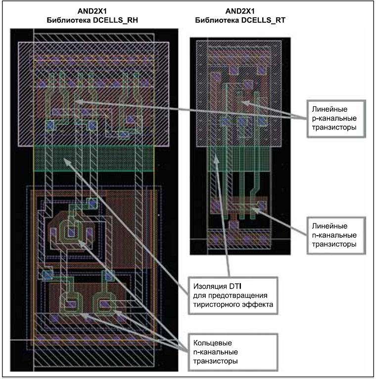
Figure 8. Examples of radiation-resistant elements AND developed by Milander using SOI BCD technology.
Figure 8 shows two options for implementing the same AND logic element for different conditions. On the left we see the full stuffing - ring transistors in individual guard rings. On the right is the simpler option, for a low total dose: linear transistors, instead of guard rings, only good contacts in the ground. And in both cases, the dielectric isolation of n-channel transistors from p-channel to protect the chip from the thyristor effect. In volumetric technology, guard rings perform this function. It should be noted that for many space applications, resistance to the full dose at the level of 50-100 crad (Si) is quite enough, and linear transistors do this very well, without requiring significant deterioration of the functional parameters of the circuit in order to achieve stability.
With single failures, the situation is this: the approximate diameter of the region from which the charge is collected when a single particle enters is of the order of one micron, that is, more than the size of a memory cell made according to deeply submicron design standards. Indeed, the so-called multiple failures are discovered experimentally, when one particle causes the switching of several bits at once. Moreover, with a decrease in design standards, the energy required to switch the memory bit also decreases, that is, more hits result in failures than for chips made according to more rough design standards. Including the ingress of alpha particles from radioactive impurities in structural materials.
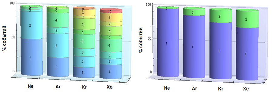
Figure 9. Comparison of the number of failures from a single particle hit for two different 6T SRAM variants in the technology with design standards of 65 nm. Source - A. Balbekov et al., “Issues of VLSI applicability for 65 nm CMOS technology under the influence of outer space factors”.
Figure 9 shows the experimental data on single faults in the 65 nm volumetric technology. On the left is the usual 6T-SRAM. Ten glitches from one hit! The Hamming code will not protect you from this. So, if we are talking about commercial microcircuits, then on rough design standards with single failures everything will be slightly better than on thin ones. At the very least, they will remain solitary, and they can really be corrected by encoding. But if the chip is specially created for space applications, then the developer’s arsenal has a huge number of architectural, circuit and topological solutions that can provide high durability at the same time as high performance. On the right side of the figure is also 6T-SRAM, with exactly the same electrical circuit, but with a different topology. The price of improvements that remove multiple crashes thyristor effect and increase resistance to the full dose - fourfold increase in area. It doesn’t sound very nice, but no one said it would be easy. Nevertheless, Radiation Hardening by Design works and allows you to achieve predetermined resistance indicators at small design standards on any volumetric technology.
Why pre-set? Because the achievement of different levels of resistance requires the use of different methods to increase it, and for each technology and technical task, the required set of methods is different. Then why not apply it all at once so that it feels good? Because the achievement of radiation resistance always occurs due to the deterioration of functional parameters (energy consumption, crystal area, speed, etc.), and they are the first priority. That is why we need clear requirements for technical specifications, both in functionality and in durability. True, microcircuits are not so often made to solve a single problem, especially radically stable, in which the circulation for each of the available applications can be several dozen pieces. But still, a good understanding of the requirements allows, for example, not to use ring transistors,
The eye of the attentive reader is probably caught on the word "volumetric" in the phrase "predefined indicators of resistance at small design standards for any volumetric technology." Is it not superfluous there? Everyone knows that radiant-resistant microcircuits need to be made using the technology “silicon on an insulator” or “silicon on sapphire”.
The technology "silicon on the insulator" has long been firmly entrenched in the glory of radiation-resistant. The roots of this popular misconception date back to antiquity, when the forerunner of the SOI, silicon on sapphire, was actively used for military development. Why? The transistors in this technology are electrically separated from each other and, more importantly, from the substrate. This means that the area of collection of radiation-induced charge upon short-term exposure of the chip to radiation with a high dose rate will be small. This, in turn, significantly reduces the time of loss of working capacity - what you need to work in an atomic war. And indeed, no other method of reducing the time of loss of working capacity, except for full dielectric isolation, does not exist.
The second important part of the myth “SOI = joy resistance” is the resistance to the thyristor effect, including when exposed to a high dose rate. The thyristor effect or “latch” is almost the main headache for developers of microchips and devices for space, and it is not surprising that the technology that allows you to get rid of it has earned fame as radiation-resistant. But in reality the situation is again somewhat more complicated.
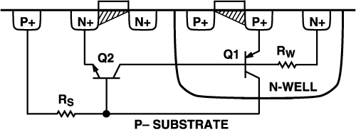
Figure 10. Cross-section of a bulk CMOS technology with a parasitic thyristor.
The cause of the thyristor effect is the parasitic thyristor structure present inside the elements of volume CMOS technology. If the resistances Rs and Rw are large enough, then this thyristor structure, when a charged particle enters, can open and short-circuit the ground of the chip with power, which, as you know, is not good. How large are these resistances in real microchips? The answer to this question is quite simple: contact to the substrate or pocket is an extra area, so they try to minimize their number. And this, in turn, means that by default the thyristor effect in the "ordinary" chip will be more likely than not. True, the thyristor effect can happen not only from radiation, but also when exposed, for example, to an electrostatic discharge or even simply from an elevated temperature and high current density with an unsuccessful topology.
In a significant part of space systems, a reboot is quite acceptable in case of unforeseen circumstances, that is, you can try to use a chip that is prone to “latching” by putting a power control circuit in the power supply and power reset if the norm is exceeded. This, in fact, is regularly done in situations where it is very necessary to use a high-performance commercial microcircuit, and the protection chips from the thyristor effect (Latchup Current Limiter) are a rather popular radiant-resistant product. But such a solution has many limitations. You can reset power not everywhere and not always, a reboot in the process of performing an important maneuver can put an end to a long mission. The current consumption of a modern microcircuit can vary many times depending on the mode of its operation, that is, consumption in the “nothing happens and there is a latch” mode may be less than in the case of regular operation in another mode. What level should the current limit be set to? It’s also not clear. The time it takes to turn off the power and prevent the destruction of the chip depends on many factors, including the specific chip. Somewhere you can not rush anywhere and reset the power as many times as necessary, but somewhere after the first or second time the chip still burns irreversibly.
In a microcircuit made using SOI technology, the thyristor effect cannot be in principle, because all transistors are electrically separated. And the best thing is that to achieve resistance to the thyristor effect, you do not need to do anything at all. That is, commercial microcircuits made according to the SOI technology are also absolutely resistant to it, which greatly facilitates their use in space. So, for example, a commercial SOI processor will control the new American Orion spacecraft.
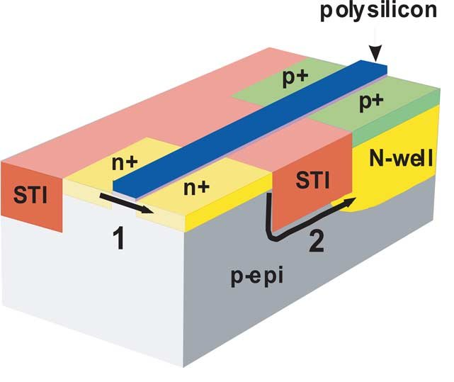
Figure 11. Radiation-induced leaks in bulk CMOS technology. Source - J. Schwank et.al., “Radiation effects in MOS oxides”, IEEE TNS, Vol. 55, No. 4, 2008
What is the problem? The fact that, in addition to the effects of dose rate and “latch”, there are still single failures and a complete absorbed dose, with which KNI technology is far from being so rosy. The figure shows two creepage paths in bulk CMOS technology. Both of these paths are easily closed with proper topological design - one using ring n-channel transistors, and the second using guard rings. These solutions have disadvantages from the point of view of the functioning of the circuit (restrictions on the minimum size of a ring transistor, loss of area when using guard rings), but from the point of view of ensuring radiation resistance they are very effective.
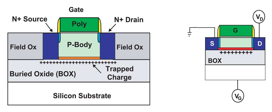
Figure 12. Additional leakage mechanism in SOI technology.
In SOI technology, there is another leak path from source to drain along the boundary of silicon and latent oxide. Hidden oxide is much thicker than the gate, which means that a lot of positive charge can accumulate in it. If we consider the “lower” transistor (the right part of Figure 12), for which the latent oxide is a gate, then we see that in the normal situation the source-gate voltage of this transistor is zero, and its threshold voltage is several tens of volts, that is no current flows through this transistor. Upon irradiation, a positive charge accumulates in the latent oxide (the geometry of the main transistor affects this process, in particular, the thickness of the silicon instrument layer), and the threshold voltage of the “lower” n-channel transistor drops. As soon as it drops below zero, the current begins to flow freely through the transistor through an uncontrolled lower channel. Thus, from the point of view of the total absorbed dose, the SOI technology is fundamentally strictly worse than the volumetric technology. But maybe there is a way to somehow rectify the situation?
Typically, the substrate of the microcircuit is grounded, but in the SOI, nothing prevents us from applying a negative voltage to it, and not the ground, and thus close the lower transistor? On the one hand, the idea is sound and it is actively used. Moreover, in the case of a fully depleted SOI (FDSOI) and norms of 45-28 nm, potential monitoring under latent oxide is also used in normal operation. On the other hand, the electric field in the latent oxide not only closes the parasitic transistor, but also accelerates the accumulation of a positive charge in the latent oxide. As a result, depending on the process parameters and the magnitude of the applied negative voltage, the dose resistance of the microcircuit with the negative voltage applied to the substrate can not only not improve, but also become worse! Further, as is usually the case, there are subtleties, but fundamentally the situation is that topological and circuit methods using volumetric technology make it possible to achieve almost any reasonable level of resistance to a full dose, and by "reasonable levels" I understand here, say 100 Mrad (Si). At SOI, there are fundamental limitations, and the level of resistance of a particular process can be quite low. You can’t get around these limitations without interfering with the technology (usually not available for commercial reasons), and you won’t be able to find out the dose resistance parameters without expensive tests. and the level of resistance of a particular process can be quite low. You can’t get around these limitations without interfering with the technology (usually not available for commercial reasons), and you won’t be able to find out the dose resistance parameters without expensive tests. and the level of resistance of a particular process can be quite low. You can’t get around these limitations without interfering with the technology (usually not available for commercial reasons), and you won’t be able to find out the dose resistance parameters without expensive tests.
The situation with single failures in the SOI is no less interesting. On the one hand, the SOI has much less volume from which the charge released when an ionizing particle enters is collected (although disputes between leading scientists have been going on for many years about the exact shape of this volume). On the other hand, the gate region (“body”) of the SOI of the MOS transistor is so small that even a small charge entering it can significantly increase the voltage in it. If the voltage rises high enough to open the pn junction source-body, then the parasitic bipolar source-body-drain transistor will turn on, and the charge introduced by the ionizing particle will be multiplied by the gain of this transistor. In practice, this means a drop in the threshold LET to levels below 1 MeV * cm ^ 2 / (mg), that is, anything will get into the chip. Of course, the parasitic thyristor effect in the SOI can be dealt with by attaching the gate region to the source of the transistor or to the ground / power. But, firstly, no one does this in commercial microcircuits (because there is no need), and secondly, contact with the body is a loss of area, especially sensitive for keys, where it should be independent. Each cache cell has at least two keys, which leads to a significant increase in the area of the cache and the crystal as a whole. At the same time, in volumetric technology, to suppress the thyristor effect and the parasitic bipolar effect, one contact on 4-8 memory cells may be enough, and even guard rings can be made with less loss of area than on contacts to the transistor body in the SOI. An important advantage of SOI in deeply submicron technologies is that that dielectric insulation prevents the spread of charge and multiple faults with high magnification, which can appear in volumetric technology. However, the track size of the ionizing particle is comparable to the size of the memory cell, and double faults in the SOI are quite recorded.
In total, the situation with radiation resistance of the silicon on insulator technology looks so that it is not “radiation resistant in itself”, but has a number of advantages and a number of disadvantages with respect to the bulk technology. Part of the disadvantages of the SOI can be circumvented with the help of special design techniques, but the same can be done with the volumetric technology. Therefore, when choosing a commercial microcircuit for use in conditions of radiation exposure, one cannot rely on SOI as a panacea, and when choosing a technology for developing a specialized radio-resistant VLSI, one must carefully weigh the pros and cons of SOI and volumetric technology to solve a specific problem and provide the required resistance levels to various radiation effects.
Hundreds of thousands of specialists around the world are working to ensure the radiation resistance of integrated circuits, and it is impossible to grasp the immensity in one popular science article. Yes, this topic is not for the article and not even for the dissertation. In any case, not for the candidate dissertation. Due to the specifics of the format, fellow specialists will find here enough simplifications, inaccuracies and maybe even actual errors. I would like it to not, but messages about necessary edits are received in PM. Without pretending to be complete and novel, I hope that I have managed to clearly describe the most popular issues related to radiation resistance and misconceptions, as well as convey to the reader the idea that microelectronics in general and space microelectronics in particular are one of the most rapidly progressing fields science and technology
Figure 1. An indispensable beautiful picture about cosmic radiation and the fragile Earth.
The most popular theses on radiation resistance used in near-space disputes look something like this:
- Radiant chips are not needed. Kubsats fly perfectly on ordinary ones, on the ISS are ordinary Lenovo laptops, in Dragon there are ordinary microcircuits, and even NASA in Orion delivered ordinary microcircuits!
- It is quite possible to put very old microcircuits on the satellites, right down to the "loose crumble", no serious performance is needed there. But without joy, nowhere, and therefore fly on junk.
- The thesis that supplements the previous one: radically stable microcircuits, in principle, cannot be done at low design standards, therefore the use of time-tested components is not only justified, but also necessary.
- In order for the microcircuit to be radiant resistant, it is necessary and sufficient to make it using the technology “silicon on an insulator” or “silicon on sapphire”.
- All “military” microcircuits are radio-resistant, and all radio-resistant microcircuits are “military”.
As you can see, some of these theses directly contradict each other - which is regularly the subject of controversy or the reason for far-reaching incorrect conclusions.
You need to start the conversation with an important disclaimer: radiation resistance is not the center of the world and the only quality that should be suitable for use in space or other aggressive environments chip. Radiation resistance is only one requirement from a long series, which includes reliability, extended temperature range, resistance to electrostatic discharge, vibration resistance - and reliable confirmation of all of the above parameters, that is, long and expensive certification. It is important everything that may not allow the chip to work out the entire required service life, and most applications of radiant-resistant chips imply the impossibility of repair or replacement. On the other hand, if something is wrong with one of the parameters, the designer of the final product can often find a way around the limitation - to place the chip that is most sensitive to the dose of radiation behind a thick wall, monitor the current consumption of the chip that is vulnerable to the thyristor effect and reset its power if necessary, or thermostat the chip with a narrow temperature range. Or it may not be found, and the only way to solve the task will be to order a new ASIC radar resistant.
It is also useful to remember that developers of special-purpose systems are the same people as any other developers. Many of them also like to write code for crust-filled crutches to yesterday’s deadline and use more powerful hardware so that it definitely works on it; some would have used Arduino if it had been properly certified. And, of course, people who set tasks for developers of special-purpose systems and developers of microcircuits for them rarely feel shy in the requirements for reliability, performance, and joy resistance. Therefore, modern design standards on satellites are still needed - I want large amounts of DRAM, multi-core processors, and the latest FPGAs. I already mentioned above that
Radiation effects
The concepts of “radiation resistance” and “radiation-resistant microcircuit” are grand simplifications. In fact, there are many different sources of ionizing radiation, and they can affect the functioning of electronic devices in different ways. Accordingly, for different applications, resistance to different sets of influencing factors and different levels of exposure is necessary, so a “stable” microcircuit designed to operate in low Earth orbit is absolutely not required to work normally when analyzing blockages in Chernobyl.
Ionizing radiation is called ionizing, because the release of energy in the volume of a substance during braking of incoming particles ionizes the substance. Each material has its own energy necessary for ionization and creation of an electron-hole pair. For silicon, this is 3.6 eV, for its oxide - 17 eV, for gallium arsenide - 4.8 eV. Also, an incoming particle may not ionize an atom, but “move” it from the right place in the crystal lattice (in silicon, this requires 21 eV to be transferred to the atom). The electron-hole pairs created in a substance can have different effects on the electrical and physical properties and on the behavior of the electrical circuit. Radiation effects can be divided into four large groups: effects of the total absorbed dose, effects of dose rate, effects caused by the ingress of single particles, and effects of displacement.
Dose effects
The total absorbed dose of radiation is measured in rad, indicating the substance that absorbs radiation. 1 rad = 0.01 J / kg, that is, the amount of energy released in a unit mass of a substance. Less commonly used is a unit of measure of Gray, equal to 100 rad (or 1 J / kg). It is important to understand that the absorbed dose in different substances will vary for the same number of ionizing particles released by the radiation source (this is the exposure dose). In the case of silicon microcircuits, the desired material is silicon oxide, because the effect on it, and not on silicon, mainly affects the electrical characteristics of the circuit, since the mobility of holes in SiO2 at normal temperature is so small that they accumulate in the oxide, creating built-in positive charge. Typical dose resistance levels of commercial microcircuits lie in the range of 5-100 krad (Si), radiation resistance levels demanded by customers start at 30 krad (Si) and end somewhere around 1 Grad (Si), depending on the purpose of the microcircuit. The lethal dose for humans is about 6 gray.
Figure 2. Examples of calculations of the set of the total absorbed dose over 10 years in various circular orbits for protection of 1 g / cm ^ 2. Source - N.V. Kuznetsov, “Radiation hazard in near-Earth orbits and interplanetary trajectories of spacecraft”.
The effects of the full dose are associated with the accumulation of this positive charge in dielectrics and are manifested in CMOS schemes in several main ways:
- The shift in the threshold voltage of transistors arising from the accumulation of a positive charge in the gate dielectric and the change in the electric field in the transistor channel. For n-channel transistors, the threshold usually decreases (but the dependence can be nonmonotonic), and for p-channel transistors it increases, and the shift value correlates with the thickness of the gate oxide, i.e., with the design standards. The thresholds of transistors in circuits with rough design standards can change so as to cause a functional failure (n-channel transistors stop closing, p-channel transistors open); in submicron technologies this effect is less important, but in analog circuits it can deliver a lot of headache.
- Uncontrolled leakage current occurs. It can flow from the source of the transistor to its own drain or to an adjacent transistor. The cause of leaks is the accumulation of a positive charge, but not in the gate insulator, but in the thick insulating material. In fact, a parasitic transistor is formed parallel to the main transistor, the gate voltage of which is controlled by a radiation dose. The manifestation of this effect is determined by the features of the geometry of the transition from a gate insulator to an insulating one, that is, to a much greater extent depends on a specific technology than on design standards.
- A decrease in the mobility of charge carriers due to the accumulation of defects on which charge carriers are scattered. The effect of this factor on submicron digital circuits on silicon is small, but it is more important for power transistors, including complex semiconductors (gallium nitride and silicon carbide).
- 1 / f increase in noise caused by spurious edge transistors. It is important for analog and radio frequency circuits. The value of this effect increases with a decrease in design standards, when the effect of the remaining dose effects decreases.
In bipolar schemes, the main dose effect is a drop in the gain caused by an increase in the base current due to leakage from the emitter to the base at the interface of silicon and passivating oxide. Another dose-specific effect for bipolar transistors is that they can (not necessarily) respond not only to the level of the dose accumulated, but also to the speed of its collection - the slower the dose is accumulated, the worse the resistance. This effect is called ELDRS (Enhanced Low Dose Rate Sensitivity) and it greatly complicates and increases the cost of testing, often not only bipolar, but also CMOS circuits - because they also sometimes have bipolar transistors and because it is easier to get everyone to test uniformly than figure out where ELDRS may be and where not.
Dose rate
Another part of the effects related to the dose rate is an ultrafast dose set at which so many electron-hole pairs are generated in the microcircuit that they do not have time to recombine, and a huge electric charge is introduced into the chip, which dissolves through the ground and power lines during significant time - for which the circuit stops working. This time is called the “loss of working time” and is the main characteristic of the resistance of a microcircuit or device to such effects. In addition, a large amount of the charge introduced into the microcircuit seriously changes the potentials of the areas connected to the ground and to the power supply - which can lead to the appearance of a thyristor effect.
It is the effects of a high dose rate — for the sake of resistance to which the technology “silicon on sapphire” and “silicon on an insulator” was originally developed, because the only way to reduce the charge introduced into the circuit is to separate the active region of the microcircuit from the volume of the substrate, not giving the charge from the substrate to participate in the process. Why are these effects important? A high dose rate over a short time is a typical consequence of a nuclear explosion.
Single effects
Single effects are not associated with prolonged exposure to radiation, but with the measurable effect of a single ionizing particle. They can be divided into two large groups:
- Nondestructive. These include failures in various kinds of storage elements (cache memory, register files, FPGA configuration memory, etc.), transients in combinational logic and in analog circuits. The main feature of this type of effects - they do not lead to physical destruction of the chip and can be fixed software or hardware. Moreover, transients are corrected by themselves after some time (the question is how large it is). Failures in memory arrays are of main practical interest, simply because they make up the lion's share of all failures due to the large amount of memory in modern microelectronic systems.
- Destructive. These include the thyristor effect and various, but, fortunately, rare effects such as piercing the gate or avalanche burnout of the transistor. Their distinguishing feature is that they irreversibly destroy the chip element. In the case of the thyristor effect, the chip can usually (but not always!) Be saved if the power is quickly reset. Destructive effects pose a serious danger to some types of flash memory and to devices with high voltages and current densities, the most important of which are power switches.
The specific energy yield of the ionizing particle is called “linear energy transfer” (LET) and is measured in MeV, transferred per unit length of the particle’s span in the material, per unit density of the material, that is, in (MeV * cm ^ 3) / (mg * cm) or (MeV * cm ^ 2) / mg. The LET is nonlinearly and nonmonotonically dependent on the particle energy and is interconnected with the mean free path, which for particles and materials relevant in microelectronics can range from hundreds of nanometers to hundreds of millimeters.
The number of particles found in space decreases with the growth of LET (see Figure 4). Important values are 30 (corresponds to iron ions) and 60 or 80 (after which the probability of the event is considered negligible). In addition, an important figure is 15 MeV * cm ^ 2 / (mg) - this is the maximum LET that the products of a nuclear reaction may have when a proton or neutron enters silicon. Protons are one of the main types of solar radiation, and although their own LET is small (tenths of a unit), they have a significant effect due to nuclear reactions and secondary ionization. Secondary ionization can occur directly in the active region, or it can be the result of a proton entering an atom of some material with a large atomic number - for example, tungsten or tantalum. Heavy elements are actively used in modern microelectronic technology, for example, to create contacts from silicon to the first metallization layer. Secondary ionization is also the reason why it is not necessary to pack chips in lead boxes to increase radiation resistance.
Figure 3. The dependence of LET on energy for different types of particles.
Separately, it is worth paying attention to helium nuclei (alpha particles) - not only because there are a lot of them in the composition of solar radiation, but also because quite a lot of sources of alpha radiation can be found in ordinary life.
Figure 4. Comparison of the number of particles of different types over a two-year mission in orbit, according to Xapsos et.al., “Model for Cumulative Solar Heavy Ion Energy and Linear Energy Transfer Spectra”, IEEE TNS, Vol. 5, No. 6., 2007
1, 30 or 60 MeV * cm ^ 2 / (mg) - how much is this? The failure threshold of a standard memory cell in 7 nm technology is much lower than unity, in 180 nm - in the range from unity to tens. The use of special circuitry allows you to raise the threshold, for example, to hundreds, but it is usually more reasonable to achieve a figure of 15 or 30 units, and filter out the remnants of rare events using noise-resistant coding. 60 units is a figure that usually appears in the requirements for resistance to destructive effects.
Displacement effects
Displacement effects are local destruction of the crystal lattice, that is, “knocking out” of an atom from its intended place. The energy required to damage the crystal lattice is usually quite large, so most passing particles do not cause this effect. But its cause may be a nuclear reaction as a result of the hit of a proton or neutron, which are many in orbit. Such local lattice defects lead to a decrease in the mobility of charge carriers, an increase in noise, and some other effects. They affect conventional CMOS chips less than “ordinary” dose effects, but dominate in solar panels, photodetectors, power transistors, as well as in complex semiconductors that do not have oxide, for example, gallium arsenide and gallium nitride. This explains their high dose resistance - they simply do not have effects that cause rapid degradation of silicon chips, and what is there is weaker and later. The amount of radiation causing bias effects is measured in particles (usually protons or neutrons) per square centimeter of chip area.
So, with a description of the influencing factors of radiation figured out, now let's see where and in what combinations they threaten microcircuits.
What? Where? When?
Figure 2 shows an example of calculating the full dose set in different orbits. Next, we need to discuss a lot of assumptions - solar activity, shape, material and thickness of protection, and so on, but in general, despite the fact that the picture is a typical spherical horse in a vacuum, the trend is clear: in different orbits, the speed of the full dose can vary by five orders of magnitude. At the same time, in low orbits, under the first belt of Van Allen, the dose is accumulated so slowly that many ordinary commercial microcircuits can withstand several years in such conditions. Yes, that microchips, even much more fragile people fly there for years without serious health consequences. Meanwhile, low orbits are almost the entire manned space program, remote sensing of the earth, satellite communications, satellite Internet promised very soon and,
Commercial microcircuits in low orbits
Actually, it is precisely because of the popularity and importance of low orbits that the legs of speculation about the fact that expensive radiant-resistant microcircuits are not needed grow, and it is quite possible to dispense with ordinary ones. But the use in space of commercial microcircuits also has pitfalls, which appear even in low orbits.
First, van Allen belts protect the Earth and its immediate surroundings only from light particles, mainly from solar electrons and protons. Heavier particles, although they are much less common, calmly fly even to our last shield - the atmosphere - and, correctly, cause single effects, including the thyristor effect, which can at any time irreversibly destroy any chip and with it the entire spacecraft . Therefore, commercial microcircuits can only be used if measures are taken to protect them from single effects.
The second problem is that the chips on the satellite are not only processors and memory, but also many other types of chips, including power and analog ones, and with their radiation resistance everything is much more complicated and much less predictable. And modern systems on a chip contain a large number of non-digital blocks; for example, for most flash memory chips, the high-voltage generator used for recording is the first to stop working, and for analog CMOS circuits, the reference voltage generated by a pair of bipolar transistors shifts, and even small leaks can seriously change the operating point of low-power analog cascades. The resistance of power keys to destructive single effects can greatly depend on the voltage applied to them, and so on and so forth.
The third important problem of using commercial microcircuits in space is that resistance to the full dose and thyristor effect is sensitive to changes in the process parameters, including small ones, so if something is changed at the factory, you can throw the results of your tests into the trash . And for commercial microcircuits, the manufacturer guarantees the stability of functional parameters, not the technological process. Moreover, in different batches you may encounter crystals from different factories; for example, the processor from the sixth iPhone, Apple A9, was made on 16 nm TSMC and 14 nm Samsung, and the user was not informed which version is on his phone. Trusted Foundry institutes or certified technical processes are used to combat this problem all over the world for the development of rain-resistant microcircuits - in short,
In total, the correct answer to the question “is it possible to use conventional commercial microcircuits in space?” Is: “Yes, it can, in some orbits and subject to a number of requirements and conditions.” Useful advice: if you still decide to use a commercial chip and invest in its testing, buy a stock immediately ten years ahead. Incidentally, this is quite a business model for a large and respected company 3DPlus - they test all commercial microchips in a row for joy, find those that have (essentially random) sufficient performance, purchase large quantities and then pack the chips in their own enclosures under their own brand .
Other orbits
However, satellites fly not only in low Earth orbit. As an example of other requirements, let's look at the only way to ensure stable communication in the vicinity of the North Pole - and this is a strategically important area for Russia - the Molniya orbit, named after the first spacecraft launched on it.
Figure 5. Orbit “Lightning”.
The main feature of this orbit is that due to its great elongation (the minimum height is about 500 km above the Earth’s surface, the maximum is up to 40,000 km, the period is 12 hours), the apparatus crosses radiation belts four times a day. The active life of the very first Molniya satellites was only about six months, primarily because of the radiation-induced drop in the power of the solar panels, which needed to power a powerful (high orbit) radio transmitter.
In geostationary orbits of navigational aids, Figure 2 promises us a dose of several hundred crad (Si) - and the dose resistance of commercial microcircuits can easily be 5-10 crad (Si), that is, about 10-15 years of active existence of such chips there can be no speech in orbit. More precisely, it can, but for this you will need a much thicker protection - or protection from something more dense than aluminum. However, here we plunge into the marvelous world of spacecraft design, so let's limit ourselves to the phrase that delivering every kilogram to orbit is expensive, and the idea of hiding the most vulnerable electronics deeper inside the case, shielding it with other components is not bad, but completely problematic won't decide.
Military chips
When dealing with the issue of debunking myths about joy resistance, it is imperative to say that you cannot equate “joy-resistant”, “space” and “military” microcircuits. Not all military microcircuits are radio-resistant, and not all radio-resistant microcircuits are military. If we turn to the American military standard Mil-Std-883 (to the American, because its Russian counterpart is classified in terms of radiation), then we will find in it many different tests for the influence of the environment - thermal cycling, humidity, air with sea salt, etc. .d. etc.
Radiations concern the following points:
1017.2 Neutron irradiation
1019.8 Ionizing radiation (total dose) test procedure
1020.1 Dose rate induced latchup test procedure
1021.3 Dose rate upset testing of digital microcircuits
1023.3 Dose rate response of linear microcircuits
Complete dose and dose rate. Single effects? No way. The technical specifications for the microcircuit may include requirements for resistance to single failures and / or thyristor effect, but these requirements are not standardized and are determined again each time, based on the needs of specific customers of each chip. It turns out that the status of "military" is not a guarantee of the ability to launch the chip into space? Yes it is. An example is the fate of the infamous “Phobos-soil”, the death of which was caused, according to the official version (very difficult to prove, but very convenient), by the hit of a heavy charged particle in the American military-class memory chip, which was not resistant to single failures .
Peace atom and others
The importance of radiation resistance is not limited to space and military applications. The natural background radiation at sea level is many times lower than even what happens in low orbit, but the Earth’s atmosphere not only serves as the last shield on the path of cosmic radiation, but also gives rise to secondary particles when interacting with it. Secondary particles are mostly neutrons. Appearing in the upper layers of the atmosphere, they usually do not reach the surface, however, at the altitudes of civilian airliners, the radiation dose is also significant and very impressive statistics are collected for single failures. X-rays are used in medicine a long time ago, and radiotherapy is one of the important ways to fight malignant tumors, and such devices also need electronics.
And, of course, do not forget that all the fuss with the lead-free solder dearly beloved by all electronic engineers was started largely due to the fact that lead and some other materials used in the manufacture of microcircuits contain impurities of heavier elements, in particular uranium, and their application leads to the generation of a small, but still well-measurable alpha particle flux - right next to vulnerable silicon. In the case of BGA-cases or 3D-assemblies - over the entire surface of vulnerable silicon.
Figure 6. Illustration of a solder ball as a source of alpha particles.
The good news is that alpha particles have a rather small mean free path in silicon (from units to tens of microns, depending on energy), and multilayer metallization helps to reduce their effect. The bad news is that at low design standards, all alpha particles that still reach silicon, cause failures, not only single, but also multiple (more on this below). For example, last year TSMC published an article at the 2018 IEEE International Reliability Physics Symposium on measuring the number of failures from pollution by alpha particles in memory according to design standards of 7 nm, that is, this problem continues to exist and requires some action in a world where everything switched to lead-free solder.
Another application of radiation-resistant circuits, which I would like to say a few words about, is high-energy physics and atomic energy. In the active zones of hadron colliders and nuclear reactors (as well as in equipment designed to eliminate radiation accidents), electronics are also needed, and it is highly desirable that one that does not need to be replaced and repaired for a considerable time. The requirements for the total absorbed dose for such applications are tens and even hundreds of Megarads (Si), that is, three orders of magnitude more than in conventional space applications. To complicate the situation, such resistance is required not from digital circuits, but from power and analog ones - electric drive control circuits and primary processing of multichannel sensors readings.
Figure 7. Normal and joy resistant reference voltage circuit. From Y. Cao et.al., “A 4.5 MGy TID-Tolerant CMOS Bandgap Reference Circuit Using a Dynamic Base Leakage Compensation Technique”, IEEE TNS, Vol.60, N.4, 2013
I will illustrate the scale of the challenges facing developers of chips for nuclear energy with my favorite example. A reference voltage source (ION) equal to the band gap of a silicon bandgap voltage reference is a relatively simple and well-known circuit. Under the influence of radiation, the parameters of bipolar transistors used as diodes change (the gain decreases due to the appearance of an emitter-base leak). As a result, the reference voltage of a conventional ION circuit, which determines the accuracy of all measurements, can shift, say, by 15–20%, which corresponds to an effective ADC resolution of two to three bits. In the circuit on the right, the reference voltage varies within 1% (which is more than 7 bits) at a dose of ionizing radiation of 4.5 MGy. In order to achieve this impressive result, the scheme had to be seriously reworked, adding a whole bunch of feedbacks to compensate for dose leakage. In the rainproof version, there are approximately four times more elements than in the normal version, and its energy consumption is twice as much. And the worst news is that for each new scheme, the radiation resistance strategy and its implementation have to be developed separately. But there is still the problem of protecting analog circuits from single effects, the solution of which is also poorly formalized.
Radiation Resistance and Design Standards
On the website of one microelectronic factory for quite a long time there was a statement that radiation resistance cannot be achieved at design standards below 600 nm, because otherwise "charged particles pierce silicon." By surprising coincidence, the minimum design standards available to that factory were just 600 nm. And one senior employee of another factory reported in an interview that making microchips for space at design standards below 90 nm was "technologically impossible." And again, it so coincided that it is technologically impossible to do something at rates below 90 nm in this particular factory. The marketing reasons for these situations and the immediate benefits from them are understandable, but in the long run, such phrases, addressed to a wide audience, seem to me to do more harm than good.
Also, there are regularly discussions that are not tied to any marketing that microchips made according to design standards are coarser than a certain limit, are immune to destructive single failures (in particular, to the thyristor effect), which means many years of use of long-old technologies are not only justified, but and necessary.
Or vice versa, phrases stating that microcircuits with design standards below 250 nm are immune to the thyristor effect, because they have such low operating voltages that the thyristor simply cannot open. Or there are opinions that in fact the problem is not in the design standards, but in the fact that the CMOS technology is fundamentally vulnerable to radiation (which is confirmed by the tests made by the applicant in the seventies), and the old radiant-resistant chips are bipolar / KNS / GaAs. And since CMOS technology is fundamentally bad, but all modern chips are made on it - this means that modern chips are not stable by definition, and the only sure way for astronautics is to invest money in bringing to mind the long-abandoned gallium arsenide (at the same time on the commercial market of Intel win) or return to time-tested discrete logic. And even better - to the lamps.
Radiant - mean old and backward?
In fairness, it should be noted that in circuits performed at design standards about a couple of microns or more, there really usually is no thyristor effect and single failures. “Usually”, however, does not mean “always” in any way, there are examples of old circuits with low resistance to thyristor effect, and design standards do not guarantee anything. A high resistance to single failures arises simply because switching elements at such design standards requires a lot of energy. During normal operation, too, so I would like to wish those who continue to use the old chips to try to assemble the Intel Core processor on the logic of the 74 series, and think about what kind of rocket will be able to lift the resulting monster into the air.
On the other hand, microelectronics are not alive by single processors. There are a huge number of tasks for which very small design standards are not needed or not so mandatory, and levels of 500-90 nm are quite enough. The global commercial market for microcircuits on wafers with a diameter of 200 mm (and these are design standards of 90 nm and higher) has been growing for several years, right up to the shortage of production equipment. Both “long-developed” and completely new microcircuits are produced on “outdated” design standards, and many factories are ready to guarantee the long-term future of technological processes (but not necessarily their complete invariance). Therefore, the “backwardness” of a particular factory from the conditional TSMC does not at all mean the impossibility of commercial success in either the civilian or the special resistant field.
The high cost of developing, manufacturing and certifying radiant-resistant circuits is an even bigger headache for manufacturers than in automotive or industrial electronics. Small circulations (and often if not hundreds, then thousands) often complicate the commercialization of such developments, because if you need to divide a million dollars into a thousand chips (the development cost is relatively simple chip by 180 nm standards), then this is a thousand dollars per a chip, but certification is still needed, which can easily result in several millions (especially if you test CMOS circuits on ELDRS). And if you need to pay back a billion dollars in a small run? That is how much development costs at 5-7 nm. The high cost of development and certification has led to that all over the world, the development of a significant part of rain-resistant microcircuits is directly or indirectly subsidized by states. This greatly reduces the number of new projects, encourages longer and more inventive to sell what is, and maximize the use of proven IP-blocks. As a result, the popular rain-resistant microcircuits are produced and used for many years, creating the illusion that all the rain-resistant microcircuits are old. And in most cases, customers are satisfied with this, because in a situation where reliability is still primary in relation to performance, reusing an already proven solution is often the best you can think of, and having a “flight heritage” is a huge competitive advantage. This also helps to extend the period of active production of successful developments - even when they are already obsolete, and when there is already a replacement. In addition, even the installation of a pin-to-pin-compatible analogue in most cases requires at least a reconciliation of the design documentation, as well as a maximum of costly tests. And this is in a situation where no development is required, so what about the case when you really need to redo something to use the new chip? Of course, in such a situation, hardware developers tend to reuse the proven solutions as a whole. when do you really need to redo something to use a new chip? Of course, in such a situation, hardware developers tend to reuse the proven solutions as a whole. when do you really need to redo something to use a new chip? Of course, in such a situation, hardware developers tend to reuse the proven solutions as a whole.
It doesn’t help public perception that the path of new developments into space is long and thorny - and even longer into the news, and it is from popular science news that ordinary people usually learn about the achievements of the space industry. In 2015, there were several messages of the form “the New Horizons satellite, which reached Pluto, has the same processor as in the Sony PlayStation”, and this prefix was already twenty years old at the time of the news release. Excellent and very competent presentation of the material, you will not say anything. New Horizons was launched in 2006, and project development began in 2000 - in the year of the first flight of the Mongoose-V processor, that is, it was the newest available processor with existing experience in orbit. The development of this processor ended in 1998, and began in 1994 - exactly simultaneously with the release of the PlayStation. Here is another example: Power750 architecture processors were released for civilian applications in 1997, and in 1998 the iMac debuted with such a processor. In 2001, the development of a rad-resistant analogue, the RAD750, was completed. This processor first hit the cosmos in 2005, and only in 2012 after the soft landing of Curiosity rover on Mars. Of course, then there were also some yellow headlines about the processor fifteen years ago, but the development of the Curiosity project began in 2003, that is, even before the first flight of the RAD750 processor. after a soft landing on Mars rover Curiosity. Of course, then there were also some yellow headlines about the processor fifteen years ago, but the development of the Curiosity project began in 2003, that is, even before the first flight of the RAD750 processor. after a soft landing on Mars rover Curiosity. Of course, then there were also some yellow headlines about the processor fifteen years ago, but the development of the Curiosity project began in 2003, that is, even before the first flight of the RAD750 processor.
Frontiers
Despite all of the above, right now the level of design standards at which the development of computing platforms for space is being conducted is 65-45-22 nm. The American RAD5500 chipset has already been put into serial production at 45 nm, the European DAHLIA processor is due out at 28 nm next year, and the ASIC development platform designed for long-term use is being actively created at 65 nm in the Belgian IMEC. Russian developers are not far behind either - the next year’s NIISI RAS roadmap shows the output of a 65-nm radiant-resistant processor, and publications on this topic speak of creating a development platform, that is, these design standards have a great future not only in Europe but also in Russia .
And even at this level of design standards, the development of rain-resistant electronics does not stop - if you look at the latest issues of IEEE Transactions on Nuclear Science, there you can find enough work on the study of transistors with design standards of 20-16-14 nm, preparing the way for new generations of space microprocessors. At these design standards, developers expect a lot of new and interesting things: firstly, ring transistors cannot be made, secondly, FinFET has a completely different channel geometry and isolation, thirdly, there are FDSOI technologies, which also have enough specificity.
Уменьшение проектных норм, безусловно, влияет на радиационную стойкость изготавливаемых на них микросхем, но вовсе не обязательно в худшую сторону. Общий тренд состоит в том, что со снижением проектных норм влияние полной дозы уменьшается, а одиночных эффектов увеличивается. Сдвиг порогового напряжения в проектных нормах 180 нм и ниже измеряется в единицах или десятках милливольт даже для больших доз: подзатворный оксид такой тонкий, что накапливающийся в нем заряд туннелирует в канал вместо того, чтобы накапливаться. Переходной слой в технологиях с изоляцией STI достаточно компактный, что позволяет во многих случаях обеспечить низкие утечки при полной дозе в несколько десятков или даже сотен крад(Si). А если применить в глубоко субмикронной объемной технологии кольцевые транзисторы и охранные кольца, то мы разом избавимся от всех дозовых проблем.
Figure 8. Examples of radiation-resistant elements AND developed by Milander using SOI BCD technology.
Figure 8 shows two options for implementing the same AND logic element for different conditions. On the left we see the full stuffing - ring transistors in individual guard rings. On the right is the simpler option, for a low total dose: linear transistors, instead of guard rings, only good contacts in the ground. And in both cases, the dielectric isolation of n-channel transistors from p-channel to protect the chip from the thyristor effect. In volumetric technology, guard rings perform this function. It should be noted that for many space applications, resistance to the full dose at the level of 50-100 crad (Si) is quite enough, and linear transistors do this very well, without requiring significant deterioration of the functional parameters of the circuit in order to achieve stability.
With single failures, the situation is this: the approximate diameter of the region from which the charge is collected when a single particle enters is of the order of one micron, that is, more than the size of a memory cell made according to deeply submicron design standards. Indeed, the so-called multiple failures are discovered experimentally, when one particle causes the switching of several bits at once. Moreover, with a decrease in design standards, the energy required to switch the memory bit also decreases, that is, more hits result in failures than for chips made according to more rough design standards. Including the ingress of alpha particles from radioactive impurities in structural materials.
Figure 9. Comparison of the number of failures from a single particle hit for two different 6T SRAM variants in the technology with design standards of 65 nm. Source - A. Balbekov et al., “Issues of VLSI applicability for 65 nm CMOS technology under the influence of outer space factors”.
Figure 9 shows the experimental data on single faults in the 65 nm volumetric technology. On the left is the usual 6T-SRAM. Ten glitches from one hit! The Hamming code will not protect you from this. So, if we are talking about commercial microcircuits, then on rough design standards with single failures everything will be slightly better than on thin ones. At the very least, they will remain solitary, and they can really be corrected by encoding. But if the chip is specially created for space applications, then the developer’s arsenal has a huge number of architectural, circuit and topological solutions that can provide high durability at the same time as high performance. On the right side of the figure is also 6T-SRAM, with exactly the same electrical circuit, but with a different topology. The price of improvements that remove multiple crashes thyristor effect and increase resistance to the full dose - fourfold increase in area. It doesn’t sound very nice, but no one said it would be easy. Nevertheless, Radiation Hardening by Design works and allows you to achieve predetermined resistance indicators at small design standards on any volumetric technology.
Why pre-set? Because the achievement of different levels of resistance requires the use of different methods to increase it, and for each technology and technical task, the required set of methods is different. Then why not apply it all at once so that it feels good? Because the achievement of radiation resistance always occurs due to the deterioration of functional parameters (energy consumption, crystal area, speed, etc.), and they are the first priority. That is why we need clear requirements for technical specifications, both in functionality and in durability. True, microcircuits are not so often made to solve a single problem, especially radically stable, in which the circulation for each of the available applications can be several dozen pieces. But still, a good understanding of the requirements allows, for example, not to use ring transistors,
The eye of the attentive reader is probably caught on the word "volumetric" in the phrase "predefined indicators of resistance at small design standards for any volumetric technology." Is it not superfluous there? Everyone knows that radiant-resistant microcircuits need to be made using the technology “silicon on an insulator” or “silicon on sapphire”.
Silicon on the insulator
The technology "silicon on the insulator" has long been firmly entrenched in the glory of radiation-resistant. The roots of this popular misconception date back to antiquity, when the forerunner of the SOI, silicon on sapphire, was actively used for military development. Why? The transistors in this technology are electrically separated from each other and, more importantly, from the substrate. This means that the area of collection of radiation-induced charge upon short-term exposure of the chip to radiation with a high dose rate will be small. This, in turn, significantly reduces the time of loss of working capacity - what you need to work in an atomic war. And indeed, no other method of reducing the time of loss of working capacity, except for full dielectric isolation, does not exist.
The second important part of the myth “SOI = joy resistance” is the resistance to the thyristor effect, including when exposed to a high dose rate. The thyristor effect or “latch” is almost the main headache for developers of microchips and devices for space, and it is not surprising that the technology that allows you to get rid of it has earned fame as radiation-resistant. But in reality the situation is again somewhat more complicated.
Figure 10. Cross-section of a bulk CMOS technology with a parasitic thyristor.
The cause of the thyristor effect is the parasitic thyristor structure present inside the elements of volume CMOS technology. If the resistances Rs and Rw are large enough, then this thyristor structure, when a charged particle enters, can open and short-circuit the ground of the chip with power, which, as you know, is not good. How large are these resistances in real microchips? The answer to this question is quite simple: contact to the substrate or pocket is an extra area, so they try to minimize their number. And this, in turn, means that by default the thyristor effect in the "ordinary" chip will be more likely than not. True, the thyristor effect can happen not only from radiation, but also when exposed, for example, to an electrostatic discharge or even simply from an elevated temperature and high current density with an unsuccessful topology.
In a significant part of space systems, a reboot is quite acceptable in case of unforeseen circumstances, that is, you can try to use a chip that is prone to “latching” by putting a power control circuit in the power supply and power reset if the norm is exceeded. This, in fact, is regularly done in situations where it is very necessary to use a high-performance commercial microcircuit, and the protection chips from the thyristor effect (Latchup Current Limiter) are a rather popular radiant-resistant product. But such a solution has many limitations. You can reset power not everywhere and not always, a reboot in the process of performing an important maneuver can put an end to a long mission. The current consumption of a modern microcircuit can vary many times depending on the mode of its operation, that is, consumption in the “nothing happens and there is a latch” mode may be less than in the case of regular operation in another mode. What level should the current limit be set to? It’s also not clear. The time it takes to turn off the power and prevent the destruction of the chip depends on many factors, including the specific chip. Somewhere you can not rush anywhere and reset the power as many times as necessary, but somewhere after the first or second time the chip still burns irreversibly.
In a microcircuit made using SOI technology, the thyristor effect cannot be in principle, because all transistors are electrically separated. And the best thing is that to achieve resistance to the thyristor effect, you do not need to do anything at all. That is, commercial microcircuits made according to the SOI technology are also absolutely resistant to it, which greatly facilitates their use in space. So, for example, a commercial SOI processor will control the new American Orion spacecraft.
Figure 11. Radiation-induced leaks in bulk CMOS technology. Source - J. Schwank et.al., “Radiation effects in MOS oxides”, IEEE TNS, Vol. 55, No. 4, 2008
What is the problem? The fact that, in addition to the effects of dose rate and “latch”, there are still single failures and a complete absorbed dose, with which KNI technology is far from being so rosy. The figure shows two creepage paths in bulk CMOS technology. Both of these paths are easily closed with proper topological design - one using ring n-channel transistors, and the second using guard rings. These solutions have disadvantages from the point of view of the functioning of the circuit (restrictions on the minimum size of a ring transistor, loss of area when using guard rings), but from the point of view of ensuring radiation resistance they are very effective.
Figure 12. Additional leakage mechanism in SOI technology.
In SOI technology, there is another leak path from source to drain along the boundary of silicon and latent oxide. Hidden oxide is much thicker than the gate, which means that a lot of positive charge can accumulate in it. If we consider the “lower” transistor (the right part of Figure 12), for which the latent oxide is a gate, then we see that in the normal situation the source-gate voltage of this transistor is zero, and its threshold voltage is several tens of volts, that is no current flows through this transistor. Upon irradiation, a positive charge accumulates in the latent oxide (the geometry of the main transistor affects this process, in particular, the thickness of the silicon instrument layer), and the threshold voltage of the “lower” n-channel transistor drops. As soon as it drops below zero, the current begins to flow freely through the transistor through an uncontrolled lower channel. Thus, from the point of view of the total absorbed dose, the SOI technology is fundamentally strictly worse than the volumetric technology. But maybe there is a way to somehow rectify the situation?
Typically, the substrate of the microcircuit is grounded, but in the SOI, nothing prevents us from applying a negative voltage to it, and not the ground, and thus close the lower transistor? On the one hand, the idea is sound and it is actively used. Moreover, in the case of a fully depleted SOI (FDSOI) and norms of 45-28 nm, potential monitoring under latent oxide is also used in normal operation. On the other hand, the electric field in the latent oxide not only closes the parasitic transistor, but also accelerates the accumulation of a positive charge in the latent oxide. As a result, depending on the process parameters and the magnitude of the applied negative voltage, the dose resistance of the microcircuit with the negative voltage applied to the substrate can not only not improve, but also become worse! Further, as is usually the case, there are subtleties, but fundamentally the situation is that topological and circuit methods using volumetric technology make it possible to achieve almost any reasonable level of resistance to a full dose, and by "reasonable levels" I understand here, say 100 Mrad (Si). At SOI, there are fundamental limitations, and the level of resistance of a particular process can be quite low. You can’t get around these limitations without interfering with the technology (usually not available for commercial reasons), and you won’t be able to find out the dose resistance parameters without expensive tests. and the level of resistance of a particular process can be quite low. You can’t get around these limitations without interfering with the technology (usually not available for commercial reasons), and you won’t be able to find out the dose resistance parameters without expensive tests. and the level of resistance of a particular process can be quite low. You can’t get around these limitations without interfering with the technology (usually not available for commercial reasons), and you won’t be able to find out the dose resistance parameters without expensive tests.
The situation with single failures in the SOI is no less interesting. On the one hand, the SOI has much less volume from which the charge released when an ionizing particle enters is collected (although disputes between leading scientists have been going on for many years about the exact shape of this volume). On the other hand, the gate region (“body”) of the SOI of the MOS transistor is so small that even a small charge entering it can significantly increase the voltage in it. If the voltage rises high enough to open the pn junction source-body, then the parasitic bipolar source-body-drain transistor will turn on, and the charge introduced by the ionizing particle will be multiplied by the gain of this transistor. In practice, this means a drop in the threshold LET to levels below 1 MeV * cm ^ 2 / (mg), that is, anything will get into the chip. Of course, the parasitic thyristor effect in the SOI can be dealt with by attaching the gate region to the source of the transistor or to the ground / power. But, firstly, no one does this in commercial microcircuits (because there is no need), and secondly, contact with the body is a loss of area, especially sensitive for keys, where it should be independent. Each cache cell has at least two keys, which leads to a significant increase in the area of the cache and the crystal as a whole. At the same time, in volumetric technology, to suppress the thyristor effect and the parasitic bipolar effect, one contact on 4-8 memory cells may be enough, and even guard rings can be made with less loss of area than on contacts to the transistor body in the SOI. An important advantage of SOI in deeply submicron technologies is that that dielectric insulation prevents the spread of charge and multiple faults with high magnification, which can appear in volumetric technology. However, the track size of the ionizing particle is comparable to the size of the memory cell, and double faults in the SOI are quite recorded.
In total, the situation with radiation resistance of the silicon on insulator technology looks so that it is not “radiation resistant in itself”, but has a number of advantages and a number of disadvantages with respect to the bulk technology. Part of the disadvantages of the SOI can be circumvented with the help of special design techniques, but the same can be done with the volumetric technology. Therefore, when choosing a commercial microcircuit for use in conditions of radiation exposure, one cannot rely on SOI as a panacea, and when choosing a technology for developing a specialized radio-resistant VLSI, one must carefully weigh the pros and cons of SOI and volumetric technology to solve a specific problem and provide the required resistance levels to various radiation effects.
Conclusion
Hundreds of thousands of specialists around the world are working to ensure the radiation resistance of integrated circuits, and it is impossible to grasp the immensity in one popular science article. Yes, this topic is not for the article and not even for the dissertation. In any case, not for the candidate dissertation. Due to the specifics of the format, fellow specialists will find here enough simplifications, inaccuracies and maybe even actual errors. I would like it to not, but messages about necessary edits are received in PM. Without pretending to be complete and novel, I hope that I have managed to clearly describe the most popular issues related to radiation resistance and misconceptions, as well as convey to the reader the idea that microelectronics in general and space microelectronics in particular are one of the most rapidly progressing fields science and technology