Sources of inspiration when developing for UDB
Well, we already know everything you need to program UDB. But it is one thing to know, and quite another to be able. Therefore, today we will discuss where and how to draw inspiration to improve our own skills, where to gain experience. As can be seen from the translation of the documentation, there is dry knowledge that is not always tied to real practice (I drew attention to this in a rather lengthy note, to the last translation to date). Actually, the statistics of article views shows that fewer and fewer people read translations. There was even a proposal to interrupt this cycle, as uninteresting, but only two parts remained, therefore, in the end, it was simply decided to reduce the pace of their preparation. In general, the documentation for the controller is a necessary thing, but not self-sufficient. Where else to get inspiration?

First of all, I can recommend the excellent document AN82156 Designing PSoC Creator Components with UDB Datapaths. In it you will find typical solutions, as well as several standard projects. Moreover, at the beginning of the document, development is carried out using the UDB Editor, and towards the end, using the Datapath Config Tool, that is, the document covers all aspects of the development. But unfortunately, looking at the price of a single PSoC chip, I would say that if it can only solve the issues described in this document, the controller is greatly overrated. PWMs and standard serial ports can be done without PSoC. Fortunately, the range of PSoC tasks is much wider. Therefore, having finished reading AN82156, we begin to look for other sources of inspiration.
The next useful source is the examples that come with PSoC Creator. I already referred to them in a note to one of the parts of the translation of company documentation (you can see here) They are stored approximately here (the disk may differ):
E: \ Program Files (x86) \ Cypress \ PSoC Creator \ 4.2 \ PSoC Creator \ psoc \ content \ CyComponentLibrary.
You should look for * .v files, that is, verilog texts, or * .vhd, since the syntax of the VHDL language requires a little more to be described, and in this language you can sometimes find interesting nuances hidden from the eyes of the programmer at Verilog. The trouble is that these are not examples, but ready-made solutions. This is wonderful, they are perfectly debugged, but we, simple programmers, have different goals with the Cypress programmers. Our task is to do something auxiliary in a short time, after which we begin to use it in our projects, which will be spent most of our time on. It should ideally solve the tasks assigned to us today, and if tomorrow we want to insert the same code into another project, where everything will be slightly different, then tomorrow we will finish it under that situation. For Cypress developers, the component is the final product, therefore, they can spend most of the time on it. And they must provide for all-all-all. So when I watched these texts, I felt sad. They are too complex for someone who has just started looking for where to draw inspiration for their first developments. But as references these texts are quite suitable. There are many valuable designs that are needed when creating your own things.
Also there are very interesting corners. For example, there are, now I’ll say in the style of “butter oil”, models for modeling (a long time ago, a stern teacher discouraged me from translating simulation in any other way than “modeling”). They can be found in the
E: \ Program Files (x86) \ Cypress \ PSoC Creator \ 4.2 \ PSoC Creator \ warp \ lib \ sim directory.
The most interesting directory for the Verilog programmer is:
E: \ Program Files (x86) \ Cypress \ PSoC Creator \ 4.2 \ PSoC Creator \ warp \ lib \ sim \ presynth \ vlg.
The description of the components in the documentation is good. But behavioral models for all standard components are described here. Sometimes this is better than the documentation (which is written in a heavy language, plus some essential details are omitted). When the behavior of this or that component is not clear, it is worth starting attempts to understand it precisely by viewing files from this directory. At first I tried to search on Google, but very often I met on the found forums only reasoning and no specifics. Here is precisely the specifics.
Nevertheless, the reference book is wonderful, but where to look for a textbook, what to learn from? Honestly, there’s nothing special. There are not many good ready-made examples for UDB Editor. I was very lucky that when I suddenly decided to play RGB LEDs, I came across a beautiful example under the UDB Editor (I wrote about it in the article that started the whole cycle). But if you work a lot with a search engine, then there will still be examples for the Datapath Config Tool, which is why I made the previous article so that everyone would understand how to use this tool. And a wonderful page on which a lot of examples are collected is located here .
On this page are developments made by third-party developers, but verified by Cypress. That is, just what we need: we are also third-party developers, but we want to learn from something that is precisely verified. Let's look at an example where I found this page - a square root hardware calculator. End users include it in the signal processing path, throwing a component onto the circuit. In this example, we will train to analyze a similar code, and then everyone will be able to start independent swimming. So, the necessary example can be downloaded from the link .
We examine it. There are examples (which everyone will consider independently) and there are libraries located in the \ CJCU_SquareRoot \ Library \ CJCU_SquareRoot.cylib directory.
For each type (integer or fixed-point) and for each bit, there is a solution. This should be noted. Versatility is good when developing in the UDB Editor, but when developing using the Datapath Edit Tool, as you can see, people are tormented like this. Do not be scared if you can’t do it universally (but if it works out the better).
At the top level (circuitry), I will not stop, we are studying not working with PSoC, but working with UDB. Let's look at an option of medium complexity - 16 bit, but integer. It is located in the directory CJCU_B_Isqrt16_v1_0.
The first thing to do is expand the transition graph of the firmware. Without it, we won’t even guess what kind of square root algorithm has been applied, since Google offers a choice of several fundamentally different algorithms.
So far, nothing is clear, but it is predictable. Need to add more information. We look at state coding. It is striking that they are not encoded in the usual incremental binary code.
I have already mentioned this approach in my articles, but I have never been able to use it in specific examples. Let me remind you that the RAM ALU dynamic configuration has only three address inputs. That is, ALU can perform one of eight operations. If the automaton has more states, then the rule “each state has its own operation” becomes impossible. Therefore, states are selected in which the operations for the ALU are identical, they have three bits supplied to the RAM address of the dynamic configuration (usually low-order ones), they are encoded in the same way, and the rest in different ways. How to add up such a solitaire is already a developer’s problem. The developers of the studied code folded exactly as shown above.
Add this information to the graph, plus color the states that perform the same function in ALU in similar colors.
No patterns have yet been manifested, but we continue to open the graph. We open Datapath Edit Tool and we study logic already in it.
Please note that we have two Datapath blocks connected in a chain. When we do something of our own, we may also need this (though the Datapath Edit Tool can create blocks that are already connected in a chain, so it's not scary):
When reading (and filling out) the graph corresponding to ALU, we always open document with the following picture:

True, the developers of this example took care of us and filled in the comment fields. Now we can use them to understand what is configured for. At the same time, we note for ourselves that writing comments is always useful both for those who will accompany the code, and for us, when in six months we will forget everything about it.
We look at the X000 code corresponding to states 0 and 12:

It’s already clear from the comment what’s happening there (the contents of register D0 are copied to register A0, and the contents of D1 are copied to register A1. Knowing this, we train our intuition for the future and find a similar entry in the fields settings:

In the same place we see that ALU works in PASS mode , the shift register is also PASS , so no other actions are really performed.
Along the way, we look at the text in Verilog and see where the value of the D0 and D1 registers is equal:

If you wish, the same can be seen in the Datapath Config Tool, by choosing View-> Initial Register Values:
For viewing, it is more convenient to directly analyze Verilog code to create of your option - work through the editor, so as not to keep in mind the syntax.
Similarly, we analyze (looking at the comments first) all the other functions of the ALU: We
redo the transition graph of the automaton taking into account new knowledge:

Something is already looming, but so far I can’t put with confidence any of the algorithms found by Google on this graph. Rather, about some you can confidently say that it’s not them, but even to the believable I still can’t give a confident answer that it’s them. Confuses the active use of registers FIFO F0 and F1. In general, in the file
\ CJCU_SquareRoot \ Library \ CJCU_SquareRoot.cylib \ CJCU_Isqrt_v1_0 \ API \ CJCU_Isqrt.c
it can be seen that F1 is used to pass the argument and return the result:
But one argument and one result. And why are there so many calls to FIFO in the course of work? And what does FIFO0 have to do with it? Cut me to pieces, but it seems that the authors took advantage of the mode that was encountered in translations of the documentation, when instead of a full-fledged FIFO, this block acted as a single register. Suppose the authors decided to expand the register set. If so, then their methodology will be useful to us in our practical work, let's study the details. In fact, the documentation talks about different approaches to working with FIFO. You can - so, you can - so, but you can - kind of. And no specifics. Again we have a chance to learn about best international practices. What do authors do with FIFO?
First, these are the signal assignments:
Secondly, here is a connection to Datapath:
From the description of the controller it is not particularly clear what all this means. But from Application Note I found out that this setting is to blame for everything:
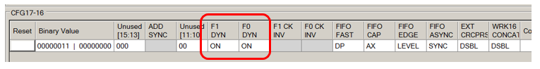
By the way, because of this setting, this block cannot be described using the UDB Editor. When these control bits are in the ON state , FIFO can work on different sources and receivers. If Dx_LOAD is equal to one, then Fx exchanges with the system bus, if zero, then with the register selected here:
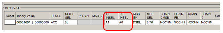
It turns out that F0 always exchanges with the register A0, and F1 in states 12 and 0 - with the system bus (to upload the result and load the argument ), in other states - with A1.
Further, from the Verilog code, we found out that in F0 the data will be loaded in states 1 and 4, and in F1 - in states 1, 3, 9, 11.
We add the acquired knowledge to the graph. In order to avoid confusion during the sequence of operations, it was also time to replace the assignment mark “a la UDB Editor” with Verilog arrows, to emphasize that the source is the value of the signal that it had before entering the block.

From the point of view of the analysis of the algorithm, everything is already clear. Before us is a modification of such an algorithm:
Only in relation to our system will it look more like this:
States 4 and 10 explicitly encode the string:
for different branches.
The line is:
it is explicitly encoded either by a pair of states 6 and 7, or a pair of states 9 and 7. For now, I want to exclaim: “Well, the inventors are the same authors!”, but very soon it will become clear why such complexity is with two branches (there is a branch in the C code and workaround).
State 2 encodes a conditional branch. State 7 encodes a loop statement. The comparison operation in step 2 is very expensive. In general, in most steps, register A0 contains the variable one. But in step 1, the variable one is unloaded into F0, and instead the value of res + one is loaded , then in step 2 the subtraction is performed for the purpose of comparison, and in steps 3 and 8, the value of one is restored . Why, in step 4, A0 is copied to F0 again, I did not understand. Perhaps this is some kind of rudiment.
It remains to figure out who res hereand who is op . We know that the condition compares op and res + one. In state 1, A0 ( one ) and A1 are added . So there A1 is res . It turns out that in state 11 A1 is also res , and it is he who gets into F1, which is fed to the output of the function. F1 in state 1 is clearly op . I propose to introduce the color differentiation of thepants of the variables. We denote res as red, op as green, and one as brown (not quite contrasted, but the other colors are even less contrasted).
Actually, the whole truth is revealed. We see how A1 famously temporarily changes from F1 to perform comparisons and calculations, how the same difference is used both for comparison (actually, generating bit C), and for participating in the formula. We even see why the empty space (bypass) in the C algorithm is encoded by a long branch of the transition graph of the automaton (in this branch, the registers are exchanged identical to the exchange occurring in the main code branch). We see everything.
The only question that never ceases to torment me is how did the authors switch FIFO to single-byte mode? The documentation says that for this you need to raise the CLR bits in the Auxiliary Control register into a unit, but I don’t see that the API has such records. Perhaps someone will understand this and write in the comments.
Well, and to develop something of their own - in the reverse order, using the acquired skills.
To develop the skills of developing “firmware” based on UDB, it is useful not only to read the documentation, but also to draw inspiration from other people's designs. The code that comes with the PSoC Creator can be useful as a reference, and the behavioral models included with the compiler will help you better understand what was meant in the documentation. The article also provides a link to a set of examples from third-party manufacturers and shows the process of parsing one of such examples.
On this, the cycle of copyright articles on working with UDB can be considered completed. I would be glad if he helped someone to obtain knowledge that is useful in practice. There are a couple of translations of documentation ahead, but statistics show that almost no one reads them. They are planned cleanly so as not to drop the topic in a nutshell.
First of all, I can recommend the excellent document AN82156 Designing PSoC Creator Components with UDB Datapaths. In it you will find typical solutions, as well as several standard projects. Moreover, at the beginning of the document, development is carried out using the UDB Editor, and towards the end, using the Datapath Config Tool, that is, the document covers all aspects of the development. But unfortunately, looking at the price of a single PSoC chip, I would say that if it can only solve the issues described in this document, the controller is greatly overrated. PWMs and standard serial ports can be done without PSoC. Fortunately, the range of PSoC tasks is much wider. Therefore, having finished reading AN82156, we begin to look for other sources of inspiration.
The next useful source is the examples that come with PSoC Creator. I already referred to them in a note to one of the parts of the translation of company documentation (you can see here) They are stored approximately here (the disk may differ):
E: \ Program Files (x86) \ Cypress \ PSoC Creator \ 4.2 \ PSoC Creator \ psoc \ content \ CyComponentLibrary.
You should look for * .v files, that is, verilog texts, or * .vhd, since the syntax of the VHDL language requires a little more to be described, and in this language you can sometimes find interesting nuances hidden from the eyes of the programmer at Verilog. The trouble is that these are not examples, but ready-made solutions. This is wonderful, they are perfectly debugged, but we, simple programmers, have different goals with the Cypress programmers. Our task is to do something auxiliary in a short time, after which we begin to use it in our projects, which will be spent most of our time on. It should ideally solve the tasks assigned to us today, and if tomorrow we want to insert the same code into another project, where everything will be slightly different, then tomorrow we will finish it under that situation. For Cypress developers, the component is the final product, therefore, they can spend most of the time on it. And they must provide for all-all-all. So when I watched these texts, I felt sad. They are too complex for someone who has just started looking for where to draw inspiration for their first developments. But as references these texts are quite suitable. There are many valuable designs that are needed when creating your own things.
Also there are very interesting corners. For example, there are, now I’ll say in the style of “butter oil”, models for modeling (a long time ago, a stern teacher discouraged me from translating simulation in any other way than “modeling”). They can be found in the
E: \ Program Files (x86) \ Cypress \ PSoC Creator \ 4.2 \ PSoC Creator \ warp \ lib \ sim directory.
The most interesting directory for the Verilog programmer is:
E: \ Program Files (x86) \ Cypress \ PSoC Creator \ 4.2 \ PSoC Creator \ warp \ lib \ sim \ presynth \ vlg.
The description of the components in the documentation is good. But behavioral models for all standard components are described here. Sometimes this is better than the documentation (which is written in a heavy language, plus some essential details are omitted). When the behavior of this or that component is not clear, it is worth starting attempts to understand it precisely by viewing files from this directory. At first I tried to search on Google, but very often I met on the found forums only reasoning and no specifics. Here is precisely the specifics.
Nevertheless, the reference book is wonderful, but where to look for a textbook, what to learn from? Honestly, there’s nothing special. There are not many good ready-made examples for UDB Editor. I was very lucky that when I suddenly decided to play RGB LEDs, I came across a beautiful example under the UDB Editor (I wrote about it in the article that started the whole cycle). But if you work a lot with a search engine, then there will still be examples for the Datapath Config Tool, which is why I made the previous article so that everyone would understand how to use this tool. And a wonderful page on which a lot of examples are collected is located here .
On this page are developments made by third-party developers, but verified by Cypress. That is, just what we need: we are also third-party developers, but we want to learn from something that is precisely verified. Let's look at an example where I found this page - a square root hardware calculator. End users include it in the signal processing path, throwing a component onto the circuit. In this example, we will train to analyze a similar code, and then everyone will be able to start independent swimming. So, the necessary example can be downloaded from the link .
We examine it. There are examples (which everyone will consider independently) and there are libraries located in the \ CJCU_SquareRoot \ Library \ CJCU_SquareRoot.cylib directory.
For each type (integer or fixed-point) and for each bit, there is a solution. This should be noted. Versatility is good when developing in the UDB Editor, but when developing using the Datapath Edit Tool, as you can see, people are tormented like this. Do not be scared if you can’t do it universally (but if it works out the better).
At the top level (circuitry), I will not stop, we are studying not working with PSoC, but working with UDB. Let's look at an option of medium complexity - 16 bit, but integer. It is located in the directory CJCU_B_Isqrt16_v1_0.
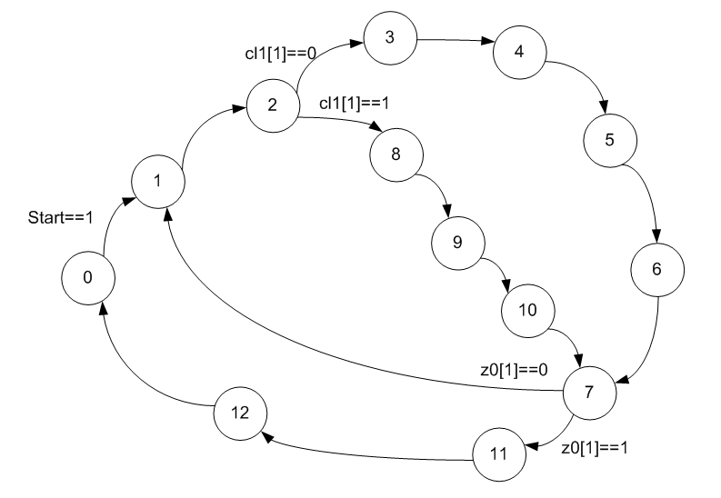
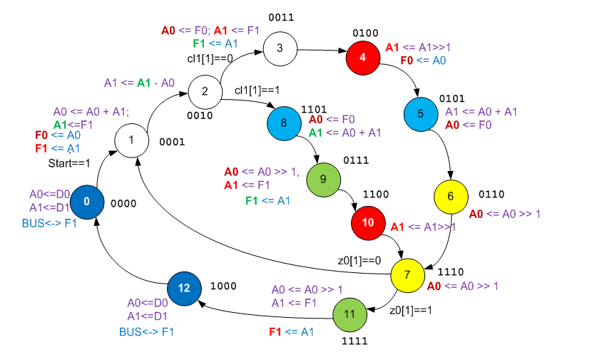
The first thing to do is expand the transition graph of the firmware. Without it, we won’t even guess what kind of square root algorithm has been applied, since Google offers a choice of several fundamentally different algorithms.
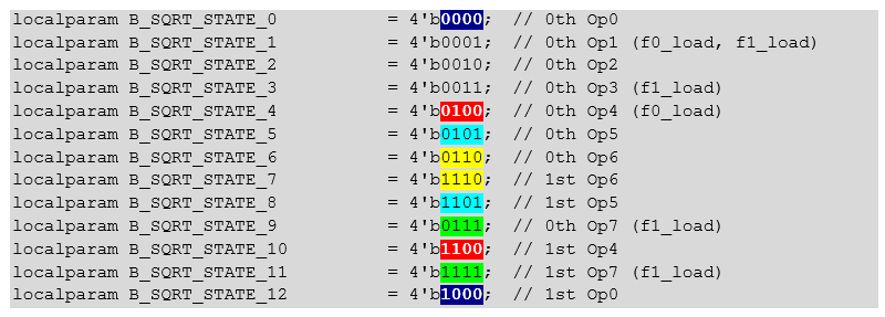
So far, nothing is clear, but it is predictable. Need to add more information. We look at state coding. It is striking that they are not encoded in the usual incremental binary code.
I have already mentioned this approach in my articles, but I have never been able to use it in specific examples. Let me remind you that the RAM ALU dynamic configuration has only three address inputs. That is, ALU can perform one of eight operations. If the automaton has more states, then the rule “each state has its own operation” becomes impossible. Therefore, states are selected in which the operations for the ALU are identical, they have three bits supplied to the RAM address of the dynamic configuration (usually low-order ones), they are encoded in the same way, and the rest in different ways. How to add up such a solitaire is already a developer’s problem. The developers of the studied code folded exactly as shown above.
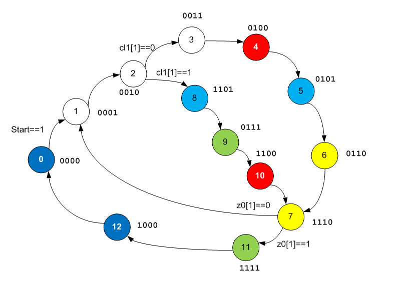
Add this information to the graph, plus color the states that perform the same function in ALU in similar colors.
No patterns have yet been manifested, but we continue to open the graph. We open Datapath Edit Tool and we study logic already in it.
Please note that we have two Datapath blocks connected in a chain. When we do something of our own, we may also need this (though the Datapath Edit Tool can create blocks that are already connected in a chain, so it's not scary):
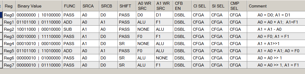
When reading (and filling out) the graph corresponding to ALU, we always open document with the following picture:
True, the developers of this example took care of us and filled in the comment fields. Now we can use them to understand what is configured for. At the same time, we note for ourselves that writing comments is always useful both for those who will accompany the code, and for us, when in six months we will forget everything about it.
We look at the X000 code corresponding to states 0 and 12:
It’s already clear from the comment what’s happening there (the contents of register D0 are copied to register A0, and the contents of D1 are copied to register A1. Knowing this, we train our intuition for the future and find a similar entry in the fields settings:
In the same place we see that ALU works in PASS mode , the shift register is also PASS , so no other actions are really performed.
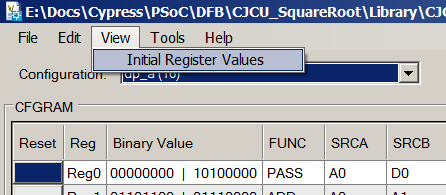
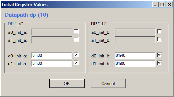
Along the way, we look at the text in Verilog and see where the value of the D0 and D1 registers is equal:
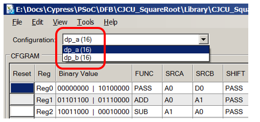
If you wish, the same can be seen in the Datapath Config Tool, by choosing View-> Initial Register Values:
For viewing, it is more convenient to directly analyze Verilog code to create of your option - work through the editor, so as not to keep in mind the syntax.
Similarly, we analyze (looking at the comments first) all the other functions of the ALU: We
redo the transition graph of the automaton taking into account new knowledge:
Something is already looming, but so far I can’t put with confidence any of the algorithms found by Google on this graph. Rather, about some you can confidently say that it’s not them, but even to the believable I still can’t give a confident answer that it’s them. Confuses the active use of registers FIFO F0 and F1. In general, in the file
\ CJCU_SquareRoot \ Library \ CJCU_SquareRoot.cylib \ CJCU_Isqrt_v1_0 \ API \ CJCU_Isqrt.c
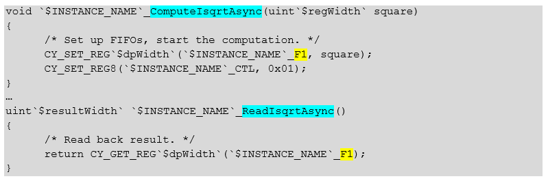
it can be seen that F1 is used to pass the argument and return the result:
Same text:
void `$INSTANCE_NAME`_ComputeIsqrtAsync(uint`$regWidth` square)
{
	/* Set up FIFOs, start the computation. */
	CY_SET_REG`$dpWidth`(`$INSTANCE_NAME`_F1, square);
	CY_SET_REG8(`$INSTANCE_NAME`_CTL, 0x01);
}
…
uint`$resultWidth` `$INSTANCE_NAME`_ReadIsqrtAsync()
{
	/* Read back result. */
	return CY_GET_REG`$dpWidth`(`$INSTANCE_NAME`_F1);
}
But one argument and one result. And why are there so many calls to FIFO in the course of work? And what does FIFO0 have to do with it? Cut me to pieces, but it seems that the authors took advantage of the mode that was encountered in translations of the documentation, when instead of a full-fledged FIFO, this block acted as a single register. Suppose the authors decided to expand the register set. If so, then their methodology will be useful to us in our practical work, let's study the details. In fact, the documentation talks about different approaches to working with FIFO. You can - so, you can - so, but you can - kind of. And no specifics. Again we have a chance to learn about best international practices. What do authors do with FIFO?
First, these are the signal assignments:
	wire f0_load = (state == B_SQRT_STATE_1 ||
					state == B_SQRT_STATE_4);
	wire f1_load = (state == B_SQRT_STATE_1 ||
					state == B_SQRT_STATE_3 ||
					state == B_SQRT_STATE_9 ||
					state == B_SQRT_STATE_11);
	wire fifo_dyn = (state == B_SQRT_STATE_0 ||
					 state == B_SQRT_STATE_12);
Secondly, here is a connection to Datapath:
        /*  input                   */  .f0_load(f0_load),
        /*  input                   */  .f1_load(f1_load),
        /*  input                   */  .d0_load(1'b0),
        /*  input                   */  .d1_load(fifo_dyn),
From the description of the controller it is not particularly clear what all this means. But from Application Note I found out that this setting is to blame for everything:
By the way, because of this setting, this block cannot be described using the UDB Editor. When these control bits are in the ON state , FIFO can work on different sources and receivers. If Dx_LOAD is equal to one, then Fx exchanges with the system bus, if zero, then with the register selected here:
It turns out that F0 always exchanges with the register A0, and F1 in states 12 and 0 - with the system bus (to upload the result and load the argument ), in other states - with A1.
Further, from the Verilog code, we found out that in F0 the data will be loaded in states 1 and 4, and in F1 - in states 1, 3, 9, 11.
We add the acquired knowledge to the graph. In order to avoid confusion during the sequence of operations, it was also time to replace the assignment mark “a la UDB Editor” with Verilog arrows, to emphasize that the source is the value of the signal that it had before entering the block.
From the point of view of the analysis of the algorithm, everything is already clear. Before us is a modification of such an algorithm:
uint32_t SquareRoot(uint32_t a_nInput)
{
    uint32_t op  = a_nInput;
    uint32_t res = 0;
    uint32_t one = 1uL << 30; // The second-to-top bit is set: use 1u << 14 for uint16_t type; use 1uL<<30 for uint32_t type
    // "one" starts at the highest power of four <= than the argument.
    while (one > op)
    {
        one >>= 2;
    }
    while (one != 0)
    {
        if (op >= res + one)
        {
            op -= res + one;
            res += one << 1;
        }
        res >>= 1;
        one >>= 2;
    }
    return res;
}
Only in relation to our system will it look more like this:
uint32_t SquareRoot(uint32_t a_nInput)
{
    uint32_t op  = a_nInput;
    uint32_t res = 0;
    uint32_t one = 1uL << 14; // The second-to-top bit is set
    while (one != 0)
    {
        if (op >= res + one)
        {
            op -= res + one;
            res += one << 1;
        }
        res >>= 1;
        one >>= 2;
    }
    return res;
}
States 4 and 10 explicitly encode the string:
res >>= 1;
for different branches.
The line is:
one >>= 2;
it is explicitly encoded either by a pair of states 6 and 7, or a pair of states 9 and 7. For now, I want to exclaim: “Well, the inventors are the same authors!”, but very soon it will become clear why such complexity is with two branches (there is a branch in the C code and workaround).
State 2 encodes a conditional branch. State 7 encodes a loop statement. The comparison operation in step 2 is very expensive. In general, in most steps, register A0 contains the variable one. But in step 1, the variable one is unloaded into F0, and instead the value of res + one is loaded , then in step 2 the subtraction is performed for the purpose of comparison, and in steps 3 and 8, the value of one is restored . Why, in step 4, A0 is copied to F0 again, I did not understand. Perhaps this is some kind of rudiment.
It remains to figure out who res hereand who is op . We know that the condition compares op and res + one. In state 1, A0 ( one ) and A1 are added . So there A1 is res . It turns out that in state 11 A1 is also res , and it is he who gets into F1, which is fed to the output of the function. F1 in state 1 is clearly op . I propose to introduce the color differentiation of the
Actually, the whole truth is revealed. We see how A1 famously temporarily changes from F1 to perform comparisons and calculations, how the same difference is used both for comparison (actually, generating bit C), and for participating in the formula. We even see why the empty space (bypass) in the C algorithm is encoded by a long branch of the transition graph of the automaton (in this branch, the registers are exchanged identical to the exchange occurring in the main code branch). We see everything.
The only question that never ceases to torment me is how did the authors switch FIFO to single-byte mode? The documentation says that for this you need to raise the CLR bits in the Auxiliary Control register into a unit, but I don’t see that the API has such records. Perhaps someone will understand this and write in the comments.
Well, and to develop something of their own - in the reverse order, using the acquired skills.
Conclusion
To develop the skills of developing “firmware” based on UDB, it is useful not only to read the documentation, but also to draw inspiration from other people's designs. The code that comes with the PSoC Creator can be useful as a reference, and the behavioral models included with the compiler will help you better understand what was meant in the documentation. The article also provides a link to a set of examples from third-party manufacturers and shows the process of parsing one of such examples.
On this, the cycle of copyright articles on working with UDB can be considered completed. I would be glad if he helped someone to obtain knowledge that is useful in practice. There are a couple of translations of documentation ahead, but statistics show that almost no one reads them. They are planned cleanly so as not to drop the topic in a nutshell.