How to make a switch?
The 14th and 15th editions of the SDSM , and in parallel with this, the work in megascale stimulated my interest in the hardware stuffing of network devices.
Now it has become curious how the equipment production process looks like, and how far Russian import substitution is in line with the ideas of the SDSM14 .
By happy nonrandomness, we still maintain close ties with Artyom Spitsyn - now the head of the Moscow office of Eltex Communications. And he offered me new questions to bring to the Okrugnaya 29B in Novosibirsk.
This article is a product of a trip to the Eltex factory and further reflection.
And we again gathered the valiant four on the campaign on Eltex: the network engineer of Yandex (I), the tester from Plesk (our Natasha), the unemployed who returned from the Around the World (Sergey, who helped us with CCIE for a year), and a student of SibGUTI IHT (Misha).
One of the things that changed in 2.5 years - allowed to take pictures. Therefore, some of the photos in this publication are provided by Eltex - of good quality, and some - in general, I'm sorry.
So in December 2018, Eltex finally launched a new building. Just a week before our coming there. There was a lot of noise, launched with aplomb. Press, ministers, excursions.
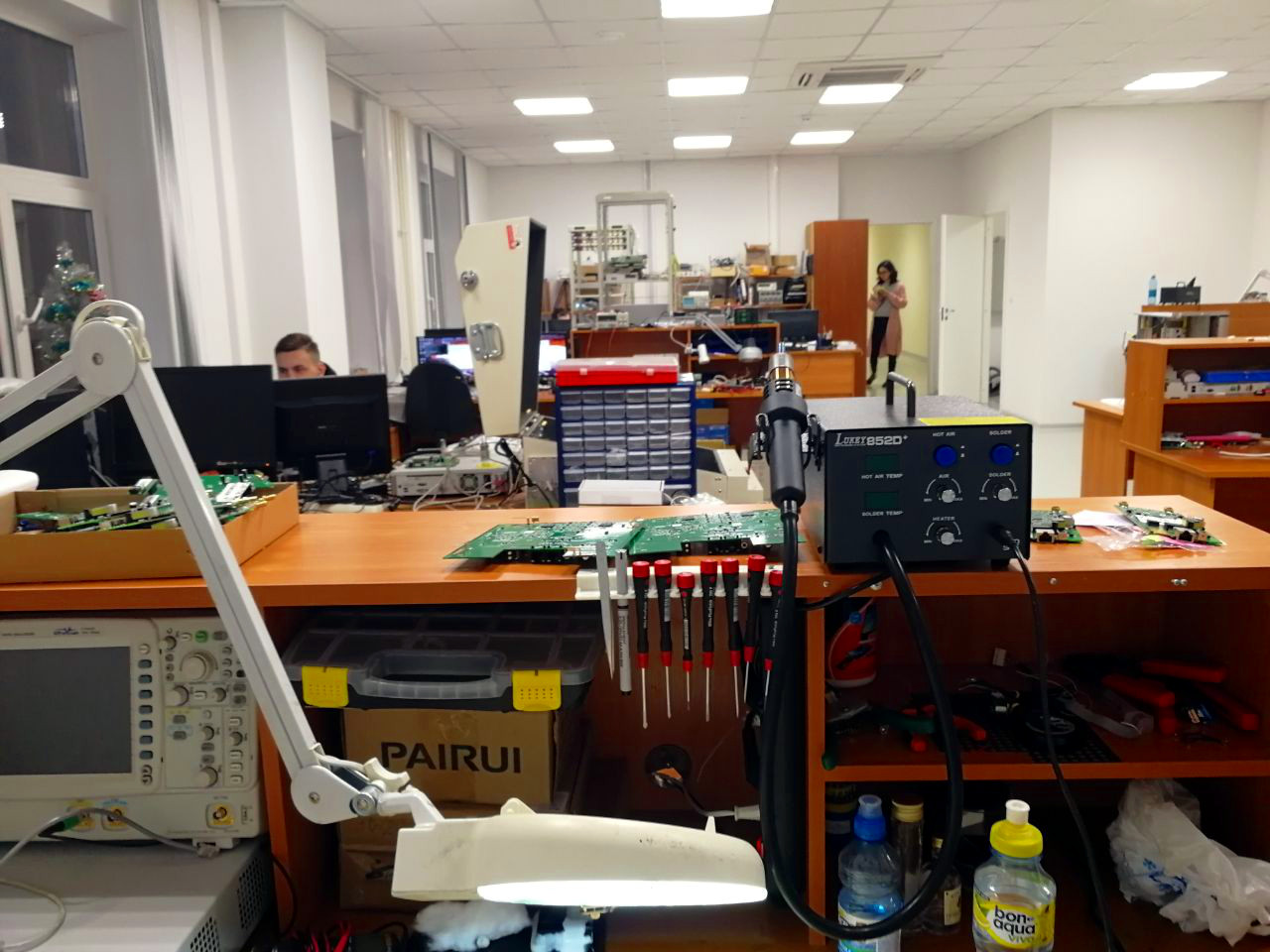
For my spoiled taste, the design is exclusively utilitarian: sterile labyrinths of corridors, monotonous cabinets, red clone tables, about which already last time was noticed. However, against this background, the lairs of designers and hardware workers, covered with boards, resistances, chips, oscilloscopes and other exciting equipment, look especially lively.
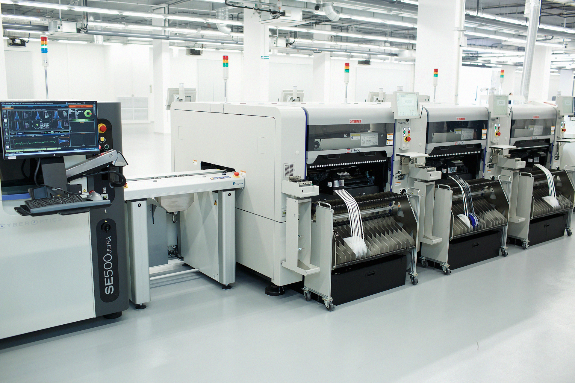
On the second floor, the first of three lines, 200 meters long
, was built . This is about a dozen of machines lined up in a row, between which a board travels along the conveyor belt, acquiring new and new details. Machines are interspersed with sites installed around the conveyor tables, where ordinary people work, doing work for which the brain and the opposed finger is cheaper than soulless Asian iron.
Thus, the line provides a complete production cycle of the product: at its beginning bare printed circuit boards enter, and at the end there is a box with a device ready for sale or installation.
Let's first take a look at the stages of production, and then we will understand what research and development work precedes this.
The first stage is the surface mounting of SMD components ( Surface Mounted Device ) - chips, resistors, capacitors and other components are installed in their places and soldered.
A PCB with already etched tracks and prepared landing sites enters the first machine from the end.
The machine applies to the board a mixture of solder and flux in the ratio of 9: 1. In order to mix only the necessary points, a pre-prepared stencil is used.
Then the board with solder moves to another machine, where components are placed on it in accordance with the scheme.
Resistors, transistors, capacitors, memory chips, packet processors, CPUs are located on reels with ribbons attached to the front side of the machine.
There are three such machines, and they are installed one after the other - all are physically identical, but have a different program and operate on different components. If rough, the grip is configured for different sizes of elements.

The next machine is an oven for baking boards. At first they warm up to 100 degrees smoothly, this equalizes the temperature of the components and protects them from thermal shock in the next production step, when the temperature rises sharply to about 330 ° C for 5 minutes. Allowable temperature regimes are specified in the specifications of the components.
At the end of the first stage, an optical analysis of the soldering takes place. In automatic mode, each board is checked for cold soldering , damage and defects.
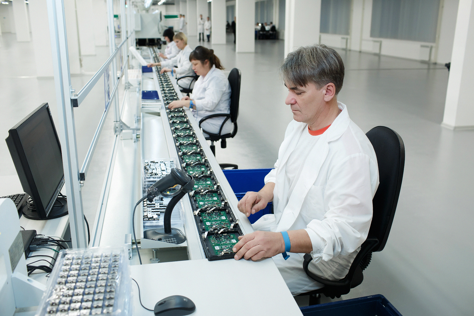
Next comes the elegance of automation. Fees fall to the mercy of gentle female (but not only) hands. In our last visit, the pin-mounting shop made an indelible impression. Fortunately, this fragrant oasis with the Amazons did not go anywhere, just a new conveyor was added in the new building.

At this stage, elements with pins are installed on the boards in ready-made holes. These include, for example, power connectors, network, buttons, LEDs.
Automation of such work is still extremely disadvantageous to a relatively small manufacturer, therefore, as before, it is carried out by people in Eltex. And since men (extremely weakly adapted to such monotonous work of creation) make many mistakes, it is entrusted mainly to women (and do not start talking about sexism - there is a historical difference between the sexes ).
Then the board goes into the furnace once again, where the installed elements are sealed using the wave method.
First, the flux is applied here, then, as in the case of surface mounting, the board heats up in three stages. And at the very end of the machine - a large tank with liquid solder and a laminar wave in the tank . The wave slightly touches one of the sides of the board, and the solder wets the contact pads, and under the action of the capillary effect rises up through the through holes, sealing the pins.
Excess solder flows back to the tank. Temperature is about 260 ° C.
On the photo board just rush into the oven.
The line was turned off shortly before our visit - the machine still retained the exciting heat, but the solder was already frozen.

Illustration from the wave soldering article
All devices further pass the firmware.

On the photo of her pass TV set-top boxes.
The next stage is the installation of the remaining elements and housing.

This is done manually: a person mounts a charge traveling along a line in a prefabricated in Asia (or Russia).
In the photo test set-top boxes.
Testing of Wi-Fi equipment looks quite interesting - metal boxes are installed on special tables, isolating radiation, and, accordingly, the influence of neighboring subjects, stuffed with measuring equipment.
The last step is to pack the finished device into protective bags, boxes and add accessories: antennas, mounting lugs, power supplies, remote controls, etc. It is engaged in this, of course, man. The assembled device comes to him along the line, and packing material is brought close to them in boxes.
The finished products are taken away to the customer.
At a particular point in time, the line is configured for a specific device: starting with programs and stencils and ending with a set of tapes with components.
If you need to change the configuration, production stops and is fully reconfigured.
In the new building, large-scale production is expected - set-top boxes, switches, routers, VoIP-gateways and VoIP-phones - something that immediately disperses to hundreds of customers of different caliber ( Contrary to stereotypes, Eltex has more than one customer ).
The old line, to which we were last time, is not dismantled, of course - there will be small-scale and experimental production on it - devices that are still required piece by piece.
But the most interesting question is not how in Asian machines the boards become overgrown with Asian components, but where the programs for them come from, the boards themselves, the stencils.
Before launching a device into production, it needs to be developed, starting with a business task and ending with a 3D simulation of the air flow inside the device and with a temperature map.
On this visit, Eltex engineers and architects were much more sociable than two years ago. I attribute this to the fact that during this time linkmeup has grown from an unknown podcast to a project that even has its own personal haters. Although it is quite possible, because last time it was four people from Huawei, who are known to send their Cossacks everywhere, and now it’s I - the janed-on, Natasha from Plesk, the unemployed Seryoga, and the student Misha).
Therefore, Eltex engineers were open and talked about their work with visible pleasure. And we, in turn, did not miss the opportunity to ask a question.
It all starts with a block diagram . This is the most superficial look at the device / board.
This scheme depicts all the elements of the board and the logical connections between them. Its task is to give an idea of the structure of the device, the role of individual parts and the interfaces of interaction between them without unnecessary detail.
So the illustration below shows the structural diagram of the motherboard of an ordinary computer

The block diagram of the motherboard ASUS P5BW-MB .
We see all its basic elements and the connections between them in the most general form.
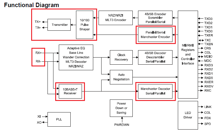
In the case of network equipment, this will be a CPU, memory, a switching chip (also known as a batch processor, it’s also Forwarding Engine), PHY (still not defined, how to pronounce - “fi” or Fai ”in Eltex all tend to the second option), etc. .
Eltex has several lines of equipment from the STB to the modular router. in a large piece of iron the operator level or DC true precepts of Juniper and Forwarding Plane completely separate from Control, so the CPU does not participate in data transmission, and assumes the intelligent functions. For switching there is Separate FE chip.
Read more e in the 14th edition SDUY .
On the other hand in the SOHO-Ruther and TV set-top boxes used SoC, which is sufficient for the functions that are expected from the device.
Each type of device has its own structural scheme.
You can lower the level of abstraction and remember that each microchip itself has a complex structure and corresponding structural and conceptual schemes. In general, the difference between the printed circuit board and the chip is that PCB with copper tracks is used as the substrate, and silicon oxide in the other.
After the structural scheme has been defined, it’s time to start choosing each specific component and developing a concept .
This is a detailed device diagram with absolutely all elements, the actual number of contacts and their connections. This is usually a multi-page document in which the scheme is divided into many parts.
But this is still the logic of the work - not wiring conductive connections on the board.
Here is an example of a small piece of the motherboard concept:
Part of the concept of the same motherboard ASUS P5BW-MB .
And here is an excerpt from the MES1124M switch circuit:
With some of the components, everything is relatively simple. Roughly speaking, resistors and capacitors are selected at nominal. Simple ASICs in their functions.
However, the more complex the chip, the more questions and compromises arise.
On the one hand, each supplier implements the same mechanisms in its own way. On the other hand, the set of supported functions is also different for everyone.
The most difficult is obviously the choice of processors - central and batch (FE). And the latter is more difficult, because for the CPU it is enough to define the architecture, and then all the manufacturers do the same thing, and for the FE, the variations on the supported functionality and the language of communication with the chip are not limited.
In addition, there are enough manufacturers on the market now:
For switches, Eltex did not stop at one in the role of FE, but uses Broadcom, Marvell and Realtek.
Both a switching chip for a switch and a SoC for some Wi-Fi point or STB is its heart, around which all other binding is built.
When the bill goes to hundreds and thousands of legs, it is worthy of scientific work to figure out how the chip works. Therefore, the manufacturer usually supplies some kind of experimental device with this chip. It should not be flexible, compact, energy efficient — its only role is to show how to interact with the chip (besides thousands of pages of the SDK documentation).
And the vendor of network equipment after that already thinks how to attach these legs to their devices.
By the way, as the software for the brownies and Fixed-size pieces of iron use this very SDK provided by the chip manufacturer. In some cases, it is finished, and sometimes given to the user - as is.
Thus, at the stage of completing the concept, it becomes finally clear how the device will work and what components are used.
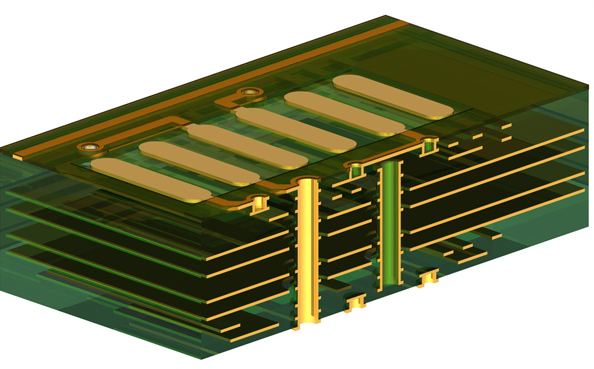
The next task is to place it all on a textolite board.
Modern boards are multi-layered - up to 40 layers (which is more rare than general practice). They are gradually increased in production - at first the scheme is etched on the deepest inner layer, then one after another the next ones are etched and pressed with the existing ones. The more layers, the smaller the thickness of each plate. Accordingly, the relationship between the number of layers and the thickness of the board is non-linear.

An example of a four-layer board: noticeably in the light, as on different layers the conductive paths and grounding fill.
Naturally, different layers should interact with each other, that is, to have a metal contact, therefore, in the right places, the layers are drilled to the required depth (to which layer you need to drill). If the diameter is greater than 0.2 mm, a conventional drill is used, with smaller values, the laser is already.
Further, this hole is metallized.
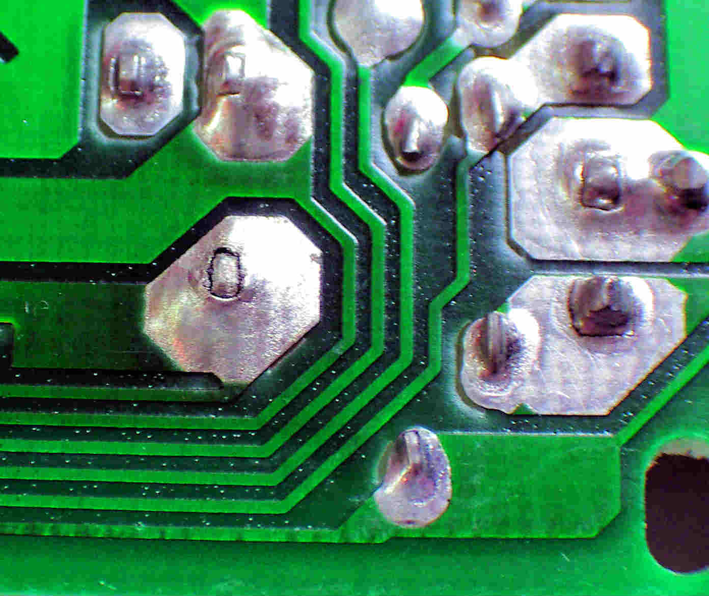
In the photo, I highlighted how such vias look on the board.
Vias
3D-model of a multilayer board and implementation of vias.
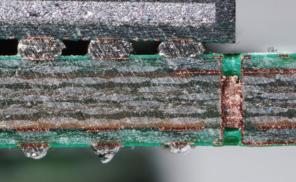
A slice of the memory board at the transition hole.
A curious moment (which, by the way, arises here at every step) - if a high-speed signal (10GE) passes through the via, let's say from the upper layer and “dives” to the inner one, then there remains an unused portion of the hole between this inner and lower layers. So let's say the stub part of the via. To get rid of it from the back side of the board, such vias are drilled with a large drill to a certain depth to the required inner layer.
A curious moment (which, by the way, occurs here at every step) - if you leave such a via as it is, the high-speed signal (10GE), diving from the upper layer to the inner one, will be reflected from the parasitic part (stub), and interference may occur to transmit interference, worsening the performance of the board up to complete malfunction.
One possible solution to this problem that Eltex uses is backdrilling technology. A counter opening of a larger diameter is drilled on the opposite side. In this case, the signal is not reflected, but passes through.
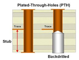
Naturally, it turns out that in the place of such an orifice on one of the layers can not run a path.
However, the general recommendation is to avoid vias as much as possible, especially for high frequency signals.
Until recently, I had the illusion that traces of tracks on printed circuit boards have long been done automatically. It was difficult to imagine that kilometers of the thinnest tracks are drawn by hand.
But first, in a podcast about virtualization, Mr. Engineer, deeply absorbed in iron, said in a tone of objection that now not a single product is able to adequately autotrace, and now Eltex has become an example confirming this statement.
Worse, initially there is not even a library of chips that could be thrown onto the workspace and connected with tracks. The specification of the chips specifies the layout of the contact pads, which is manually recreated in the project.
And if, for example, the chip has 1200 contacts, then the contacts themselves and the tracks from each are drawn manually.
In general, modern platforms for developing boards have the functionality of autotrails, only for their adequate operation, it is necessary to set hundreds of rules in the case of a more or less complex scheme.
Some of them are quite simple:
And the other part is less obvious.
Not only the trajectories of each of the thousands of tracks are determined manually, but also all vias, roundings, control of the same length of conductors where required (Read below about differential pairs ).
Pavel Bombizov, design engineer Eltex, showed how to select tracks, look at their length and compare with the length of its pair, how to choose a joint and smooth it along the radius, how to create contact pads of chips in the form of a uniform array of points.
New housing components really need to be drawn by hand. In the documentation for the chip manufacturer specifies the layout of the pads, their sizes and other information that needs to be redrawn into the library component. Sometimes it is not so easy to do this, since the number of contacts of a microcircuit can reach several thousand, and the main thing here is not to be mistaken with their location and designation.
However, then once drawn component is added to the library, and in the future it can be simply transferred to the workspace.
That is, only new components are drawn that were not used in projects before. The main part of the components is either already drawn earlier, or is available in the standard component library built into the CAD system.
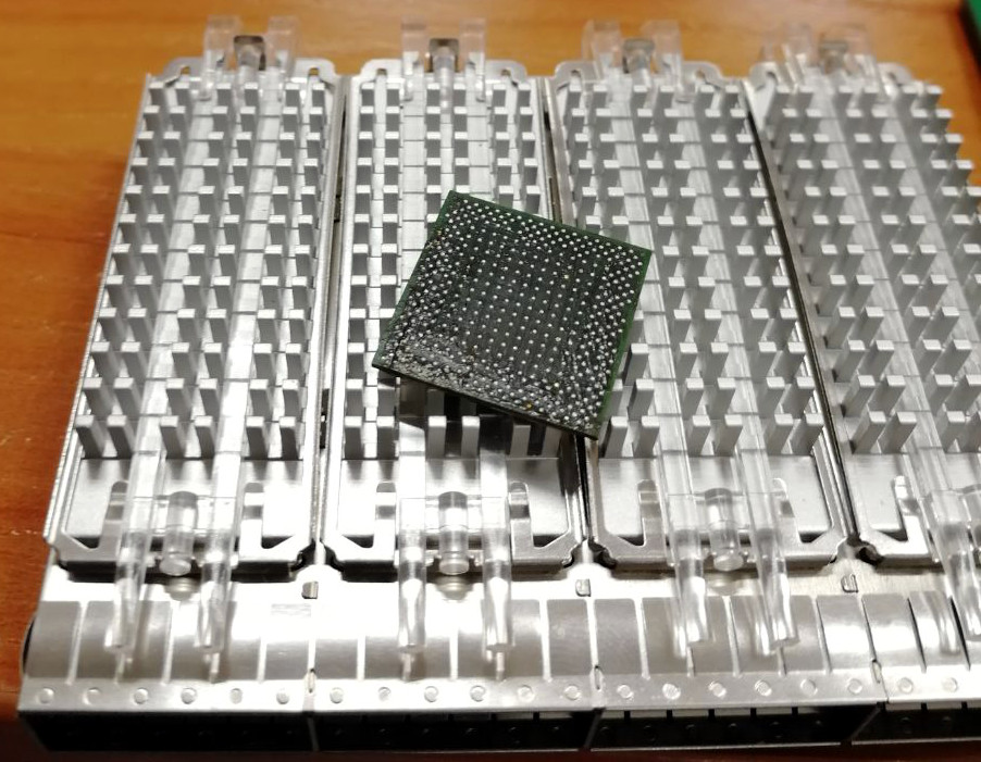
Marvelovsky PHY chip on the reverse side - for estimating the number of contacts that need to be drawn correctly .
According to Paul, the layout of one board goes away from the month. If it is a switch with a four-layer card - about one month. And for example, MES9032, having 20 layers, many nuances and requiring the solution of many constructive tasks, may require more than six months).
The final step in the design of the board is silk-screen printing - placement of component tags, connectors, input-output interfaces, and so on.
This is not only a mandatory requirement for the industrial development of boards, but also a kind of “code comments”:
How to use the board, how to install the component, where is the power supply plus / minus, what the indicator shows, even how to locate the board in the device (for example, a gyro sensor, for which the location of the axes is important).
At this stage, there is already a complete understanding of how the board will look and what components where it will stand on.
However, the development of the device is not yet complete. Even the PCB can not be sent to production, because the results of the next step may require more changes.
Further (actually in parallel) the project is transferred to the designers of the housing and ventilation system. Obviously, these are related things, therefore one person (or department) deals with them.
At this stage, the results of the previous stage are imported to SolidWorks.
From the point of view of the shape of the case, it is important to know the dimensions of the board, the location of ports, indicators, buttons, antenna leads, and so on.
From the point of view of the ventilation system, the amount of heat released by the components, their size and location.
Now a three-dimensional model of the device is being built together with the case and the inner gasket.
Based on heat dissipation, expected air flow and experience, the designer places ventilation holes, radiators and partitions and starts the calculation.
But above all, the model is greatly simplified. Cleaned:
Simplified model MES1124M.
The temperature map, the direction of air flow, their speed and all this for different time intervals are calculated for quite a long time. For a simple switch or STB on a near-video card, this takes several hours. And for the ME5000 modular router - 2 weeks.
Unfortunately, the amazingly beautiful results of calculations with air flow trajectories and temperature maps, which aroused the lively interest of any engineer, were not allowed to be published.
Alas, Eltex has no sufficient need for a computing cluster, therefore a desktop designer works for the benefit of the customer. I forgot to ask, but it would not be more convenient to contact public clouds here - every self-respecting provider already has a farm with a GPU (or plans to).
Based on the first results, the designer tries various configurations of radiators, partitions, fans, and openings within the limits.
It is not always possible, therefore, in some cases, you have to return the project a step back and revise the arrangement of elements and even their models.
This iterative process continues until the calculations show a stable temperature.
Of course, the cooling system is one of the compromise solutions between energy efficiency and the nominal temperature mode of operation.
For example, in TV set-top boxes the cooler will look out of place. At the same time, no one expects passive cooling from the fifteen-unit chassis. By the way, there are 6 such fans in it, each of which, at maximum speed, comes off the table surface:

I want to remember Yandex , which, thanks to competent planning of air flows in the servers (not only this, of course) achieved in their DC free-cooling and PUE close to one .
Well, and then comes the stage of testing the theory of practice. Before the serial production of the case in the Eltex itself, a trial version is printed on the 3D printer; a prototype of the board is placed in it. And then the device is subjected to numerous tests.
Here you can find inconsistencies of the case with the board, errors in the arrangement of elements,usability , and most importantly, to measure the real temperature of the chips and in different parts of the board, finding out how the model corresponds to reality.
According to Eltex employees, in most cases no deviations are detected. However, if the tests did not pass, the model has to be corrected - either they did not take into account something, or an error crept into the input data, for example, the chip's heat dissipation was incorrectly entered.
As for the model, then as always - it is a compromise between its proximity to reality and the efficiency of calculations. The simulated object should be simplified as much as possible, but not more.
When the tests are completed, the hull is approved, the device is working properly, it starts up in a series.
3d model of MES1124M in the case.
Plastic enclosures are made mainly in China. Metal bending and we seem to be able, although not always, as Eltex tells.
Multilayer boards are also produced in Asia, although we also have plants in Russia. This choice is due to several reasons. For example, technical process capabilities: our transition holes of 0.1 mm are not yet able to do. Product stability and predictable delivery times are other reasons. Well, nowhere to put the fact that production in Asia is still cheaper than in Russia.
All crumbling and microchips are also from there.
Well, all this is already assembled on the assembly line in Novosibirsk.
To do this, create:
This is all expected to do the same guys that are engaged in the development.
This is a printed circuit board made in China.

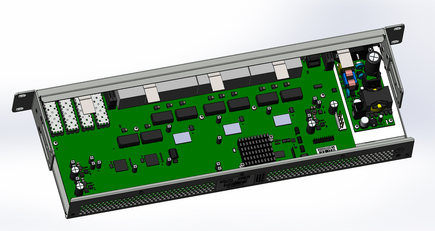
Switch Board MES1124M. On it, I noted the key components: CPU and memory, FE and PHY chips, Downlink and Uplink ports, and interestingly, transformers. Their role here is to isolate the connector contact circuits from the rest of the switch and housing circuits and, as a result, protect expensive PHY chips and packet switching chips.
1500 VAC isolation is the minimum requirement of the IEEE802.3 standard, so if 220 VAC hits a port (for example, through a twisted pair cable if the insulation of the cable is damaged), it will not burn anything - 220 VAC cannot break through.
However, the transformer cannot protect against electrostatic discharge, since the discharge from the primary side of the transformer is induced on the circuit on the secondary side. Electrostatic protection is performed by other means.
As for the import substitution, alas, we have to admit that further wiring of printed circuit boards and assembly / soldering of the finished device, we have not gone. All microchips are still being purchased in Asia.
Eltex had (and still has) experience with Baikals as central processors. Interaction with experts of Baikal Electronics is conducted when creating equipment for government agencies.
However, with packet processors (FE), the situation has not changed - we still do not know how.And, as far as I know, we are not trying. Eltex says that I am mistaken, but without details, alas. Unless, of course, this is not Milandra 's chips , which are certainly curious, but still far from the bleeding edge.
In addition, this time we had the opportunity to speak with Alexander Evgenievich Mokhov, the head of the laboratory of Ethernet Technology for the second time. In a sense, MES switches and ME5000 routers come out of his hands.
The last time we were scouts from Huawei, which we were not warned in advance. And now the visit was coordinated in advance, and guests from understandable places. Therefore, instead of mistrustful phrases, a private conversation turned out, from which it became clear that, in general, Eltex followed the best practices in the construction of modular devices.
Perhaps essentially nothing to add here.
In terms of technology, the excursion was excellent. Personally, it was interesting for me to plunge into the processes, besides, it made me read a little about this topic myself. Several things have become real discoveries, others just put everything in its place.
Despite the ambiguous attitude of both engineers of operators and ordinary users to Eltex, I am glad that we have people who are able to create such things, create them, and are not afraid to talk about them.
During this time, the modular router has gone out of development and is working on the network of an unnamed customer. If there are happy engineers who exploit them, write comments.
According to the marketing department of Eltex, today, in addition to Russia, their equipment is supplied to the CIS countries, Europe, the Middle East, North and South America, and Southeast Asia. The greatest demand in the foreign market is used by broadband access equipment for telecom operators.
Well, we wish our producer an active and productive expansion into the international market - only there healthy competition poses real challenges.
Now it has become curious how the equipment production process looks like, and how far Russian import substitution is in line with the ideas of the SDSM14 .
By happy nonrandomness, we still maintain close ties with Artyom Spitsyn - now the head of the Moscow office of Eltex Communications. And he offered me new questions to bring to the Okrugnaya 29B in Novosibirsk.
This article is a product of a trip to the Eltex factory and further reflection.
And we again gathered the valiant four on the campaign on Eltex: the network engineer of Yandex (I), the tester from Plesk (our Natasha), the unemployed who returned from the Around the World (Sergey, who helped us with CCIE for a year), and a student of SibGUTI IHT (Misha).
One of the things that changed in 2.5 years - allowed to take pictures. Therefore, some of the photos in this publication are provided by Eltex - of good quality, and some - in general, I'm sorry.
So in December 2018, Eltex finally launched a new building. Just a week before our coming there. There was a lot of noise, launched with aplomb. Press, ministers, excursions.
For my spoiled taste, the design is exclusively utilitarian: sterile labyrinths of corridors, monotonous cabinets, red clone tables, about which already last time was noticed. However, against this background, the lairs of designers and hardware workers, covered with boards, resistances, chips, oscilloscopes and other exciting equipment, look especially lively.
Production Line
On the second floor, the first of three lines, 200 meters long
, was built . This is about a dozen of machines lined up in a row, between which a board travels along the conveyor belt, acquiring new and new details. Machines are interspersed with sites installed around the conveyor tables, where ordinary people work, doing work for which the brain and the opposed finger is cheaper than soulless Asian iron.
Thus, the line provides a complete production cycle of the product: at its beginning bare printed circuit boards enter, and at the end there is a box with a device ready for sale or installation.
Let's first take a look at the stages of production, and then we will understand what research and development work precedes this.
Surface mount
The first stage is the surface mounting of SMD components ( Surface Mounted Device ) - chips, resistors, capacitors and other components are installed in their places and soldered.
A PCB with already etched tracks and prepared landing sites enters the first machine from the end.
The machine applies to the board a mixture of solder and flux in the ratio of 9: 1. In order to mix only the necessary points, a pre-prepared stencil is used.
Then the board with solder moves to another machine, where components are placed on it in accordance with the scheme.
Resistors, transistors, capacitors, memory chips, packet processors, CPUs are located on reels with ribbons attached to the front side of the machine.
There are three such machines, and they are installed one after the other - all are physically identical, but have a different program and operate on different components. If rough, the grip is configured for different sizes of elements.
The next machine is an oven for baking boards. At first they warm up to 100 degrees smoothly, this equalizes the temperature of the components and protects them from thermal shock in the next production step, when the temperature rises sharply to about 330 ° C for 5 minutes. Allowable temperature regimes are specified in the specifications of the components.
At the end of the first stage, an optical analysis of the soldering takes place. In automatic mode, each board is checked for cold soldering , damage and defects.
Pin mounting
Next comes the elegance of automation. Fees fall to the mercy of gentle female (but not only) hands. In our last visit, the pin-mounting shop made an indelible impression. Fortunately, this fragrant oasis with the Amazons did not go anywhere, just a new conveyor was added in the new building.
At this stage, elements with pins are installed on the boards in ready-made holes. These include, for example, power connectors, network, buttons, LEDs.
Automation of such work is still extremely disadvantageous to a relatively small manufacturer, therefore, as before, it is carried out by people in Eltex. And since men (extremely weakly adapted to such monotonous work of creation) make many mistakes, it is entrusted mainly to women (and do not start talking about sexism - there is a historical difference between the sexes ).
Then the board goes into the furnace once again, where the installed elements are sealed using the wave method.
First, the flux is applied here, then, as in the case of surface mounting, the board heats up in three stages. And at the very end of the machine - a large tank with liquid solder and a laminar wave in the tank . The wave slightly touches one of the sides of the board, and the solder wets the contact pads, and under the action of the capillary effect rises up through the through holes, sealing the pins.
Excess solder flows back to the tank. Temperature is about 260 ° C.
On the photo board just rush into the oven.
The line was turned off shortly before our visit - the machine still retained the exciting heat, but the solder was already frozen.
Illustration from the wave soldering article
Firmware
All devices further pass the firmware.
On the photo of her pass TV set-top boxes.
Installation in the case
The next stage is the installation of the remaining elements and housing.
This is done manually: a person mounts a charge traveling along a line in a prefabricated in Asia (or Russia).
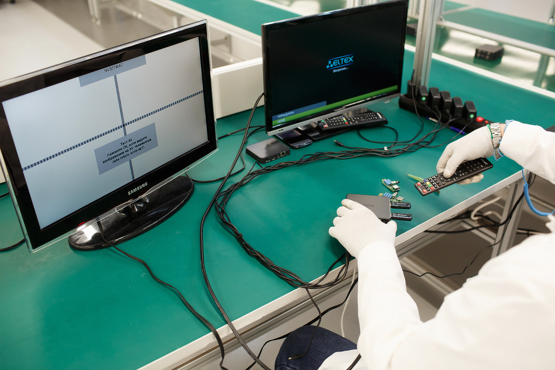
Testing
In the photo test set-top boxes.
Testing of Wi-Fi equipment looks quite interesting - metal boxes are installed on special tables, isolating radiation, and, accordingly, the influence of neighboring subjects, stuffed with measuring equipment.
Packaging
The last step is to pack the finished device into protective bags, boxes and add accessories: antennas, mounting lugs, power supplies, remote controls, etc. It is engaged in this, of course, man. The assembled device comes to him along the line, and packing material is brought close to them in boxes.
The finished products are taken away to the customer.
At a particular point in time, the line is configured for a specific device: starting with programs and stencils and ending with a set of tapes with components.
If you need to change the configuration, production stops and is fully reconfigured.
In the new building, large-scale production is expected - set-top boxes, switches, routers, VoIP-gateways and VoIP-phones - something that immediately disperses to hundreds of customers of different caliber ( Contrary to stereotypes, Eltex has more than one customer ).
The old line, to which we were last time, is not dismantled, of course - there will be small-scale and experimental production on it - devices that are still required piece by piece.
But the most interesting question is not how in Asian machines the boards become overgrown with Asian components, but where the programs for them come from, the boards themselves, the stencils.
Before launching a device into production, it needs to be developed, starting with a business task and ending with a 3D simulation of the air flow inside the device and with a temperature map.
PCB Development
On this visit, Eltex engineers and architects were much more sociable than two years ago. I attribute this to the fact that during this time linkmeup has grown from an unknown podcast to a project that even has its own personal haters. Although it is quite possible, because last time it was four people from Huawei, who are known to send their Cossacks everywhere, and now it’s I - the janed-on, Natasha from Plesk, the unemployed Seryoga, and the student Misha).
Therefore, Eltex engineers were open and talked about their work with visible pleasure. And we, in turn, did not miss the opportunity to ask a question.
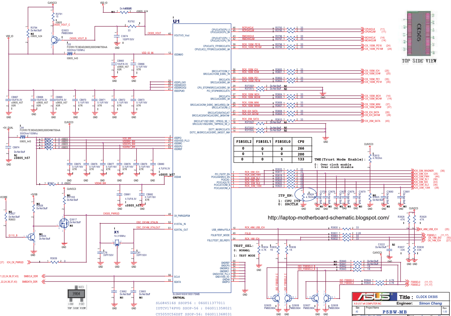
Structural scheme
It all starts with a block diagram . This is the most superficial look at the device / board.
This scheme depicts all the elements of the board and the logical connections between them. Its task is to give an idea of the structure of the device, the role of individual parts and the interfaces of interaction between them without unnecessary detail.
So the illustration below shows the structural diagram of the motherboard of an ordinary computer
The block diagram of the motherboard ASUS P5BW-MB .
We see all its basic elements and the connections between them in the most general form.
In the case of network equipment, this will be a CPU, memory, a switching chip (also known as a batch processor, it’s also Forwarding Engine), PHY (still not defined, how to pronounce - “fi” or Fai ”in Eltex all tend to the second option), etc. .
Eltex has several lines of equipment from the STB to the modular router. in a large piece of iron the operator level or DC true precepts of Juniper and Forwarding Plane completely separate from Control, so the CPU does not participate in data transmission, and assumes the intelligent functions. For switching there is Separate FE chip.
Read more e in the 14th edition SDUY .
On the other hand in the SOHO-Ruther and TV set-top boxes used SoC, which is sufficient for the functions that are expected from the device.
Each type of device has its own structural scheme.
You can lower the level of abstraction and remember that each microchip itself has a complex structure and corresponding structural and conceptual schemes. In general, the difference between the printed circuit board and the chip is that PCB with copper tracks is used as the substrate, and silicon oxide in the other.
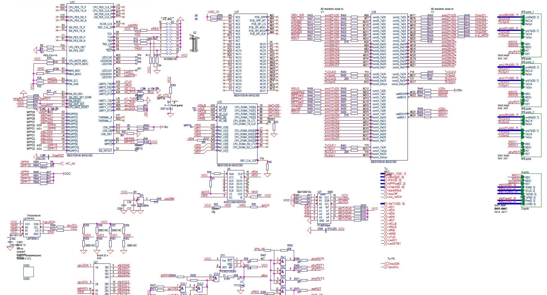
Schematic diagram
After the structural scheme has been defined, it’s time to start choosing each specific component and developing a concept .
This is a detailed device diagram with absolutely all elements, the actual number of contacts and their connections. This is usually a multi-page document in which the scheme is divided into many parts.
But this is still the logic of the work - not wiring conductive connections on the board.
Here is an example of a small piece of the motherboard concept:
Part of the concept of the same motherboard ASUS P5BW-MB .
And here is an excerpt from the MES1124M switch circuit:
With some of the components, everything is relatively simple. Roughly speaking, resistors and capacitors are selected at nominal. Simple ASICs in their functions.
However, the more complex the chip, the more questions and compromises arise.
On the one hand, each supplier implements the same mechanisms in its own way. On the other hand, the set of supported functions is also different for everyone.
The most difficult is obviously the choice of processors - central and batch (FE). And the latter is more difficult, because for the CPU it is enough to define the architecture, and then all the manufacturers do the same thing, and for the FE, the variations on the supported functionality and the language of communication with the chip are not limited.
In addition, there are enough manufacturers on the market now:
- Broadcom Series
- Marvell XPliant
- Barefoot tofino
- Mellanox Spectrum
- Innovium Teralynx
- Even Realtek
For switches, Eltex did not stop at one in the role of FE, but uses Broadcom, Marvell and Realtek.
Both a switching chip for a switch and a SoC for some Wi-Fi point or STB is its heart, around which all other binding is built.
When the bill goes to hundreds and thousands of legs, it is worthy of scientific work to figure out how the chip works. Therefore, the manufacturer usually supplies some kind of experimental device with this chip. It should not be flexible, compact, energy efficient — its only role is to show how to interact with the chip (besides thousands of pages of the SDK documentation).
And the vendor of network equipment after that already thinks how to attach these legs to their devices.
By the way, as the software for the brownies and Fixed-size pieces of iron use this very SDK provided by the chip manufacturer. In some cases, it is finished, and sometimes given to the user - as is.
Thus, at the stage of completing the concept, it becomes finally clear how the device will work and what components are used.
PCB layout
The next task is to place it all on a textolite board.
Modern boards are multi-layered - up to 40 layers (which is more rare than general practice). They are gradually increased in production - at first the scheme is etched on the deepest inner layer, then one after another the next ones are etched and pressed with the existing ones. The more layers, the smaller the thickness of each plate. Accordingly, the relationship between the number of layers and the thickness of the board is non-linear.
In the simplest case - layer one. In the simple case - there are four of them, and they are divided functionally: signal, power supply, grounding. In complex cards, such as for switches, it is also an opportunity to multiply the available area for conductors without actually increasing the size, as well as to avoid induction between adjacent tracks on the same layer, passing next to each other.
An example of a four-layer board: noticeably in the light, as on different layers the conductive paths and grounding fill.
Naturally, different layers should interact with each other, that is, to have a metal contact, therefore, in the right places, the layers are drilled to the required depth (to which layer you need to drill). If the diameter is greater than 0.2 mm, a conventional drill is used, with smaller values, the laser is already.
Further, this hole is metallized.
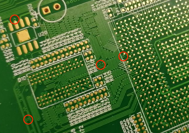
In the photo, I highlighted how such vias look on the board.
Vias
3D-model of a multilayer board and implementation of vias.
A slice of the memory board at the transition hole.
A curious moment (which, by the way, arises here at every step) - if a high-speed signal (10GE) passes through the via, let's say from the upper layer and “dives” to the inner one, then there remains an unused portion of the hole between this inner and lower layers. So let's say the stub part of the via. To get rid of it from the back side of the board, such vias are drilled with a large drill to a certain depth to the required inner layer.
A curious moment (which, by the way, occurs here at every step) - if you leave such a via as it is, the high-speed signal (10GE), diving from the upper layer to the inner one, will be reflected from the parasitic part (stub), and interference may occur to transmit interference, worsening the performance of the board up to complete malfunction.
One possible solution to this problem that Eltex uses is backdrilling technology. A counter opening of a larger diameter is drilled on the opposite side. In this case, the signal is not reflected, but passes through.
Naturally, it turns out that in the place of such an orifice on one of the layers can not run a path.
However, the general recommendation is to avoid vias as much as possible, especially for high frequency signals.
Until recently, I had the illusion that traces of tracks on printed circuit boards have long been done automatically. It was difficult to imagine that kilometers of the thinnest tracks are drawn by hand.
But first, in a podcast about virtualization, Mr. Engineer, deeply absorbed in iron, said in a tone of objection that now not a single product is able to adequately autotrace, and now Eltex has become an example confirming this statement.
Worse, initially there is not even a library of chips that could be thrown onto the workspace and connected with tracks. The specification of the chips specifies the layout of the contact pads, which is manually recreated in the project.
And if, for example, the chip has 1200 contacts, then the contacts themselves and the tracks from each are drawn manually.
In general, modern platforms for developing boards have the functionality of autotrails, only for their adequate operation, it is necessary to set hundreds of rules in the case of a more or less complex scheme.
Some of them are quite simple:
- Width of conductive tracks. There is a sea of nuances. But universal rules follow from Ohm's law: the lower the cross section, the higher the resistance and the greater the voltage drop, and accordingly the heating.
- Clearance width. With different potentials in two conductors, even a dielectric can become a conductor. And the more likely than the conductors closer.
Thus, the width of the tracks and the gaps is a trade-off between risk and efficiency.
By the way, there is a subtle point here: while all (no) Russia uses millimeters for calculating dimensions, China (and not he alone) counts in miles.
Mille - a thousandth of an inch or 0.0254 mm, respectively.
This is where the imperial system of measures lurked us, as if 8 dimensions hiding inside the elementary particles (I wonder if I’ll manage to regret this belief in life ).
Therefore, situations when working with Chinese manufacturers have to be recalculated from one system to another are quite typical. Conveniently. So at one time the Greeks transferred the numbers to the Babylonian system, because it was convenient to count in it, and then back to the Greek - because it was so accepted.
And the other part is less obvious.
- It is not recommended to make turns of the tracks at an angle of 90 degrees - it is more correct under 45 or rounded along the radius.
Otherwise, the current spreads unevenly . At high currents, this may cause local overheating and burnout of the track.
In the case of dealing with a high-speed signal, it is necessary to flip the signal on the board as smoothly as possible to reduce its attenuation, and here it is not allowed to turn even at 45 degrees - just rounding.
Eltex uses bend radius on the eye, which is more than enough. - In some areas it is required that the length of the conductors be the same.
One example would be connecting the RAM.
The other is differential pairs connecting the high-speed port (10GE) to the PHY chip. In this method, the signal is transmitted via two conductors, but one of them is inverted (with a different sign). The receiver compares the two signals received by different paths, and not the signal of a single wire to ground. In this case, electromagnetic interference affects two wires simultaneously, which increases stability, which is very important at such speeds.
Obviously, in order for the receiver to have the same signal, this signal must come at the same time, respectively, and the length of the conductors must be the same.
CPU + DDR MES1124M cards.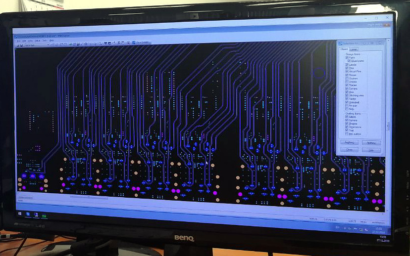
Fee, you're just a space!
This sometimes explains the strange shapes of the tracks on the boards. This is nothing but the alignment of the lengths of the conductors between themselves.
The paths connecting the processor and RAM
There is always a need for this.
CRAY-1 vector supercomputer.
Not only the trajectories of each of the thousands of tracks are determined manually, but also all vias, roundings, control of the same length of conductors where required (Read below about differential pairs ).
Pavel Bombizov, design engineer Eltex, showed how to select tracks, look at their length and compare with the length of its pair, how to choose a joint and smooth it along the radius, how to create contact pads of chips in the form of a uniform array of points.
New housing components really need to be drawn by hand. In the documentation for the chip manufacturer specifies the layout of the pads, their sizes and other information that needs to be redrawn into the library component. Sometimes it is not so easy to do this, since the number of contacts of a microcircuit can reach several thousand, and the main thing here is not to be mistaken with their location and designation.
However, then once drawn component is added to the library, and in the future it can be simply transferred to the workspace.
That is, only new components are drawn that were not used in projects before. The main part of the components is either already drawn earlier, or is available in the standard component library built into the CAD system.
Marvelovsky PHY chip on the reverse side - for estimating the number of contacts that need to be drawn correctly .
During the tour it was not very clear why Eltex hand-made alignments and bends. Software for distributing boards has been able for a very long time at least in comparing the length of conductors, alignment, setting curvature parameters. But later Eltex gave comments.That is, the design of the boards is still a colossal work, which requires the designer to be extremely accurate and focused.
Alignment of signals is done automatically, but it is easier and faster to do it manually. It all depends on the case.
For example, the memory, which in the photo of the Track linking the processor and the operational memory "is divorced automatically, so it’s problematic to draw manually.
But the diffpars in the picture of the Board , you are just a space!" aligned manually, and here it is necessary to align only one and copy the alignment to all others.
According to Paul, the layout of one board goes away from the month. If it is a switch with a four-layer card - about one month. And for example, MES9032, having 20 layers, many nuances and requiring the solution of many constructive tasks, may require more than six months).
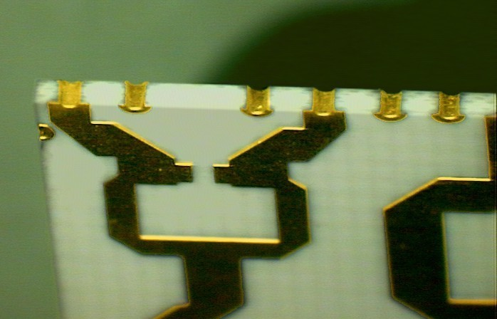
The final step in the design of the board is silk-screen printing - placement of component tags, connectors, input-output interfaces, and so on.
This is not only a mandatory requirement for the industrial development of boards, but also a kind of “code comments”:
How to use the board, how to install the component, where is the power supply plus / minus, what the indicator shows, even how to locate the board in the device (for example, a gyro sensor, for which the location of the axes is important).
At this stage, there is already a complete understanding of how the board will look and what components where it will stand on.
However, the development of the device is not yet complete. Even the PCB can not be sent to production, because the results of the next step may require more changes.
Calculation of the hull and ventilation system
Further (actually in parallel) the project is transferred to the designers of the housing and ventilation system. Obviously, these are related things, therefore one person (or department) deals with them.
At this stage, the results of the previous stage are imported to SolidWorks.
From the point of view of the shape of the case, it is important to know the dimensions of the board, the location of ports, indicators, buttons, antenna leads, and so on.
From the point of view of the ventilation system, the amount of heat released by the components, their size and location.
Now a three-dimensional model of the device is being built together with the case and the inner gasket.
Based on heat dissipation, expected air flow and experience, the designer places ventilation holes, radiators and partitions and starts the calculation.
But above all, the model is greatly simplified. Cleaned:
- Layered board
- Tracks
- Vias
- Mounting holes
- Components that emit negligible heat and do not affect air flow
- The components themselves are also simplified down to parallelepipeds.
Simplified model MES1124M.
The temperature map, the direction of air flow, their speed and all this for different time intervals are calculated for quite a long time. For a simple switch or STB on a near-video card, this takes several hours. And for the ME5000 modular router - 2 weeks.
Unfortunately, the amazingly beautiful results of calculations with air flow trajectories and temperature maps, which aroused the lively interest of any engineer, were not allowed to be published.
Alas, Eltex has no sufficient need for a computing cluster, therefore a desktop designer works for the benefit of the customer. I forgot to ask, but it would not be more convenient to contact public clouds here - every self-respecting provider already has a farm with a GPU (or plans to).
Based on the first results, the designer tries various configurations of radiators, partitions, fans, and openings within the limits.
It is not always possible, therefore, in some cases, you have to return the project a step back and revise the arrangement of elements and even their models.
This iterative process continues until the calculations show a stable temperature.
Of course, the cooling system is one of the compromise solutions between energy efficiency and the nominal temperature mode of operation.
For example, in TV set-top boxes the cooler will look out of place. At the same time, no one expects passive cooling from the fifteen-unit chassis. By the way, there are 6 such fans in it, each of which, at maximum speed, comes off the table surface:
I want to remember Yandex , which, thanks to competent planning of air flows in the servers (not only this, of course) achieved in their DC free-cooling and PUE close to one .
Well, and then comes the stage of testing the theory of practice. Before the serial production of the case in the Eltex itself, a trial version is printed on the 3D printer; a prototype of the board is placed in it. And then the device is subjected to numerous tests.
Here you can find inconsistencies of the case with the board, errors in the arrangement of elements,usability , and most importantly, to measure the real temperature of the chips and in different parts of the board, finding out how the model corresponds to reality.
According to Eltex employees, in most cases no deviations are detected. However, if the tests did not pass, the model has to be corrected - either they did not take into account something, or an error crept into the input data, for example, the chip's heat dissipation was incorrectly entered.
As for the model, then as always - it is a compromise between its proximity to reality and the efficiency of calculations. The simulated object should be simplified as much as possible, but not more.
When the tests are completed, the hull is approved, the device is working properly, it starts up in a series.
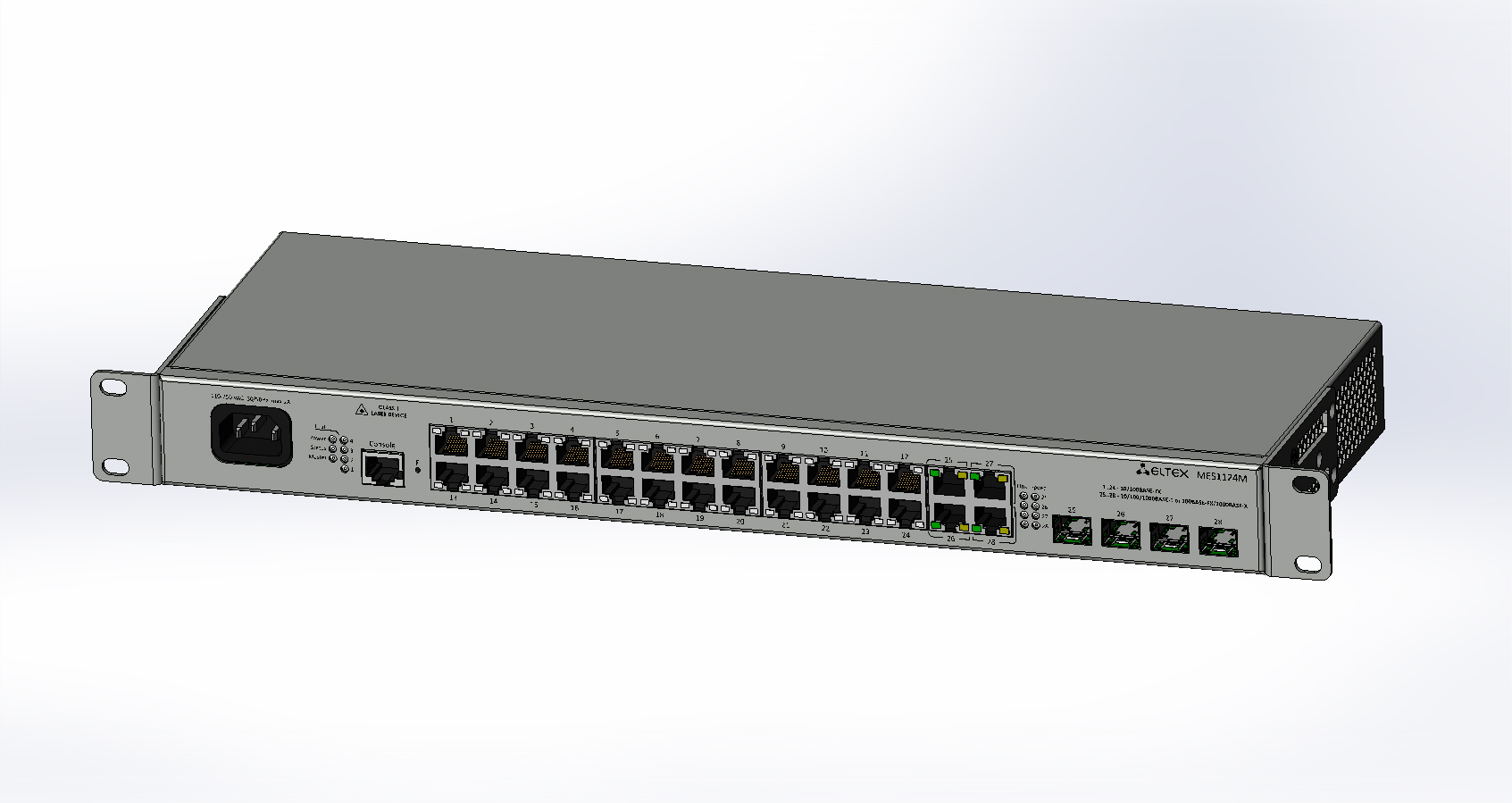
3d model of MES1124M in the case.
Plastic enclosures are made mainly in China. Metal bending and we seem to be able, although not always, as Eltex tells.
Multilayer boards are also produced in Asia, although we also have plants in Russia. This choice is due to several reasons. For example, technical process capabilities: our transition holes of 0.1 mm are not yet able to do. Product stability and predictable delivery times are other reasons. Well, nowhere to put the fact that production in Asia is still cheaper than in Russia.
All crumbling and microchips are also from there.
Well, all this is already assembled on the assembly line in Novosibirsk.
To do this, create:
- assembly drawing on the board,
- stencils for applying solder paste on the machine,
- component installer program: what, how and where to install
This is all expected to do the same guys that are engaged in the development.
This is a printed circuit board made in China.
Switch Board MES1124M. On it, I noted the key components: CPU and memory, FE and PHY chips, Downlink and Uplink ports, and interestingly, transformers. Their role here is to isolate the connector contact circuits from the rest of the switch and housing circuits and, as a result, protect expensive PHY chips and packet switching chips.
1500 VAC isolation is the minimum requirement of the IEEE802.3 standard, so if 220 VAC hits a port (for example, through a twisted pair cable if the insulation of the cable is damaged), it will not burn anything - 220 VAC cannot break through.
However, the transformer cannot protect against electrostatic discharge, since the discharge from the primary side of the transformer is induced on the circuit on the secondary side. Electrostatic protection is performed by other means.
As for the import substitution, alas, we have to admit that further wiring of printed circuit boards and assembly / soldering of the finished device, we have not gone. All microchips are still being purchased in Asia.
Eltex had (and still has) experience with Baikals as central processors. Interaction with experts of Baikal Electronics is conducted when creating equipment for government agencies.
However, with packet processors (FE), the situation has not changed - we still do not know how.
In addition, this time we had the opportunity to speak with Alexander Evgenievich Mokhov, the head of the laboratory of Ethernet Technology for the second time. In a sense, MES switches and ME5000 routers come out of his hands.
The last time we were scouts from Huawei, which we were not warned in advance. And now the visit was coordinated in advance, and guests from understandable places. Therefore, instead of mistrustful phrases, a private conversation turned out, from which it became clear that, in general, Eltex followed the best practices in the construction of modular devices.
Perhaps essentially nothing to add here.
useful links
- PCB layout
- 7 rules for the design of printed circuit boards
- Automated wave soldering and wave soldering in the technology of through mounting of printed circuit boards
- Full cycle of development of IoT pool heater control device on ESP8266 in Arduino environment
- Software PHY for Ethernet 10BASE-T
- Modern chips - a view from the inside
- From sand to processor
- Prospects for the development of Ethernet solutions
- Advanced Ethernet Switch from Milandr
Conclusion
In terms of technology, the excursion was excellent. Personally, it was interesting for me to plunge into the processes, besides, it made me read a little about this topic myself. Several things have become real discoveries, others just put everything in its place.
Despite the ambiguous attitude of both engineers of operators and ordinary users to Eltex, I am glad that we have people who are able to create such things, create them, and are not afraid to talk about them.
During this time, the modular router has gone out of development and is working on the network of an unnamed customer. If there are happy engineers who exploit them, write comments.
According to the marketing department of Eltex, today, in addition to Russia, their equipment is supplied to the CIS countries, Europe, the Middle East, North and South America, and Southeast Asia. The greatest demand in the foreign market is used by broadband access equipment for telecom operators.
Well, we wish our producer an active and productive expansion into the international market - only there healthy competition poses real challenges.
If you bring something new to the network world and you have something to show and tell, we will gladly visit you too.
Thank you
- Maria Mishchenko - Eltex marketing specialist and our guide.
- Artyom Spitsyn - head of the Moscow office of Eltex Communications and initiator of the tour.
- Pavel Bombizov - Design Engineer Eltex (circuit board design)
- Alexey Filon - Eltex Design Engineer (design of buildings and ventilation systems)
- Sergey Igonin - head of the SMD Eltex site (production line)
- Vyacheslav Gorbach - Eltex software engineer (Hardware laboratory, a story about using the SDK for SoC)
- Alexander Mokhov - head of the Ethernet laboratory of Techntex Eltex (development of network equipment and interaction with chip manufacturers)
- Roman Guryev - electronics engineer (for correction of inaccuracies)
- Dmitry Bulygin - communication engineer (for meeting Artyom and comments on the readability of the text)
- Sergey Lunkov - network engineer (for the company)
- Natalia Astashenko - tester (for the company and the amendments to the article)
- Mikhail Purtov - student (for company)
- Pavel Ostapenko - Communication Engineer (for photos that were not taken and amendments to the article)