What will be the next generation of video cards
 If a desktop computer or laptop is focused on new and demanding video games, as well as working with computer-aided design systems and other specialized applications, then it most often has a video accelerator from either Nvidia or AMD. The current generation of video accelerators is represented by the nine hundredth series of GeForce and the three hundredth series of Radeon chips. Both are gradually being filled with models of different directions: Nvidia began to do this in the fall of 2014, AMD - last June .
 A new line will appear in 2016. Manufacturers provide meager information on new products. Perhaps they fear the effect of Osborne: a story about a more perfect follower will age the current model in public perception, which will negatively affect the sales of the latter. And even the developers themselves may not know what the final product will look like on the counter. But there is some information now.
The new generation can be characterized by the use of HBM2 (High Bandwidth Memory 2) and a decrease in the manufacturing process. AMD and Nvidia are switching from 28 nm to 14 and 16 nm FinFET, respectively. Both innovations are designed to increase performance per watt by 2 times.
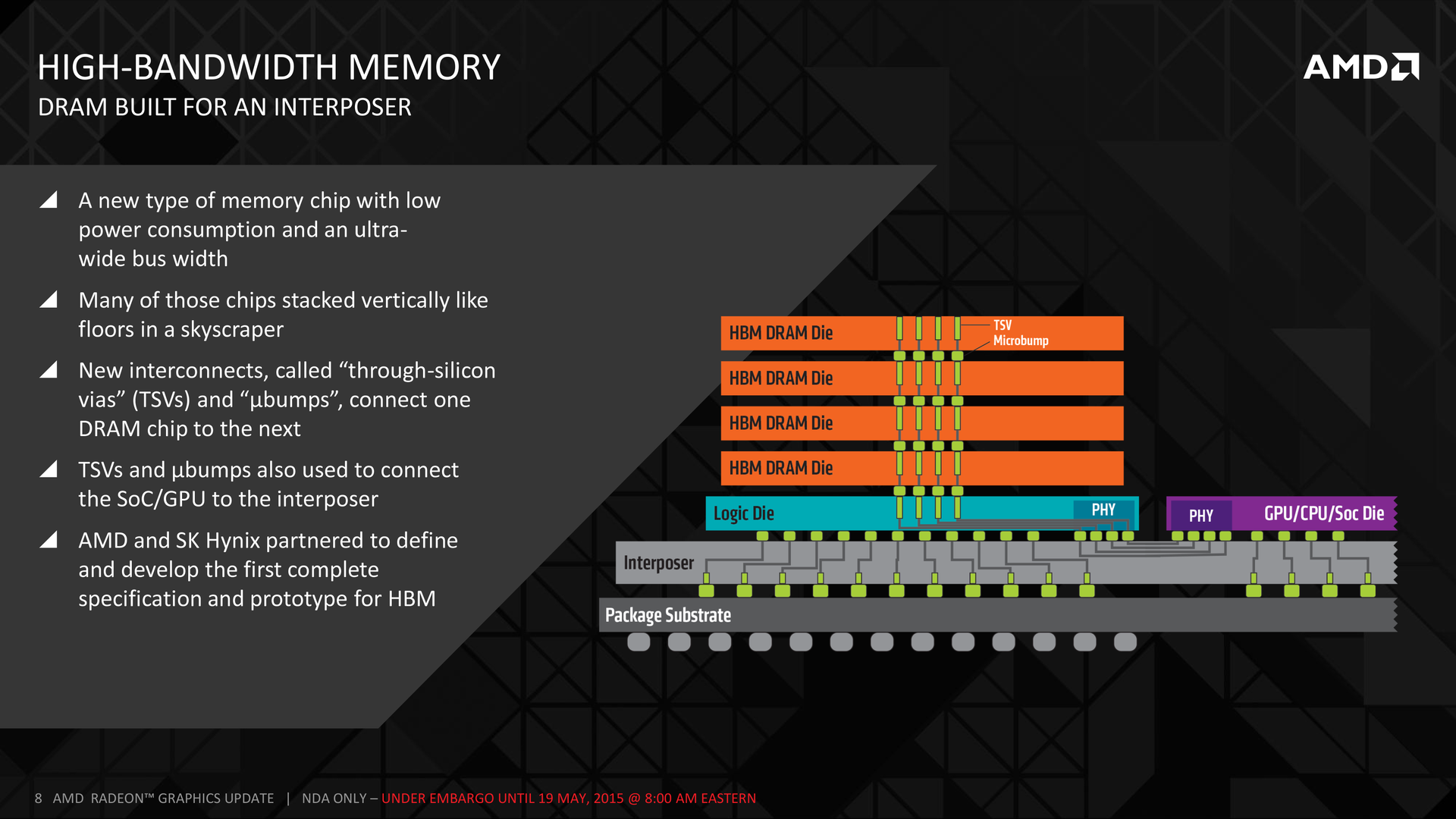
High Bandwidth Memory or HBM is a memory technology that has been developedAMD and Hynix. Before HBM, video cards used GDDR5 memory. To get additional bandwidth, I had to add chips and channels that consumed board space and energy. The usual acceleration of the frequency of the memory chips has slowed down, since increasing the frequency means a rapid increase in heat dissipation. The solution to the problem is to become what manufacturers have been doing for the last couple of decades to reduce cost and energy consumption and increase productivity: integration. For example, central processors have included many elements, from mathematical coprocessors to memory controllers. In each case, there were pluses.
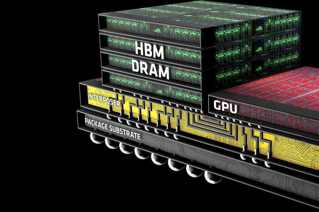
HBM involves converging the memory and video accelerator chip in one structure. But the production processes are too different to realize this in a single crystal. Therefore, a construction of three elements is used: the main chip (in this case, the GPU, video accelerator), memory columns and the interposer. Interposer is a common silicon chip manufactured by a relatively old process. The role of the interposer is completely passive. It has no active elements, since its main task is to electrically connect the tracks between the memory and the processor.
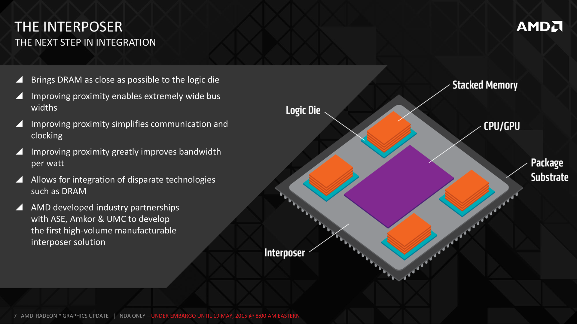
The main chip and memory columns are on the interposer. Since it is a silicon chip, it can connect much more elements than a regular board. It is the interposer that is the key detail of High Bandwidth Memory. There are other traditional elements beneath the interposer, but their task is to exchange with the PCI Express bus, output to monitors and other interfaces. All communication between the video processor and the memory takes place using an interposer. The memory frequency is not high (1 GHz instead of 6), but this is compensated by a very wide connection: 1024 bits of bus for each of the four stacks. The GDDR5 memory bus reaches 512 bits wide, which is eight times less than 4096 bits HBM. As a result, already in the first generation of HBM it turns out to demonstrate the advantage of bandwidth (512 GB / s). Hynix HBM2 production plans.
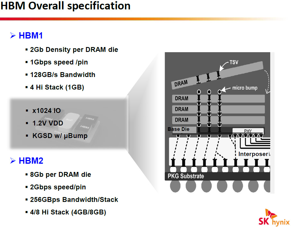
The first generation of HBM is already used in several products of the three hundredth series of Radeon. The second generation of HBM will appear in both AMD and Nvidia products. Some sources believe that owning HBM will give AMD priority access to HBM2. In it, the exchange rate will increase from 128 GB / s to 256 GB / s for each of the stacks, and the amount of memory in the layer will grow four times. The first HBM provides 4 layers of memory per stack; in the second, configurations with 4 and 8 layers will be available.
The following Nvidia microarchitecture is called Pascal. Its main features are 16-nm FinFET + process technology from TSMC and up to 16 GB of HBM2 memory. This suggests that a configuration with 4 layers of HBM2 will be used. Information is also available that the development of the next Nvidia video processor aims to achieve 1 TB / s data exchange speed with video memory. That's twice as much as the current Fury X can offer. Pascal-based cards will use NVLink for the first time, a high-speed bus between the CPU and GPUs or between GPUs. NVLink speed is significantly higher than PCI Express.
Pascal products will start shipping sometime in 2016. (It will be interesting to see the marketing of the GTX 1080 model and the explanation that it is great for 4K resolutions.) Something already exists. Nvidia recently introduced the Drive PX 2 car computer , the core of which is two Tegra processors and two certain Pascal microarchitecture chips. Drive PX 2 is a powerful number grinder for testing robotic technology, and the name Pascal is mentioned in passing in the announcement.
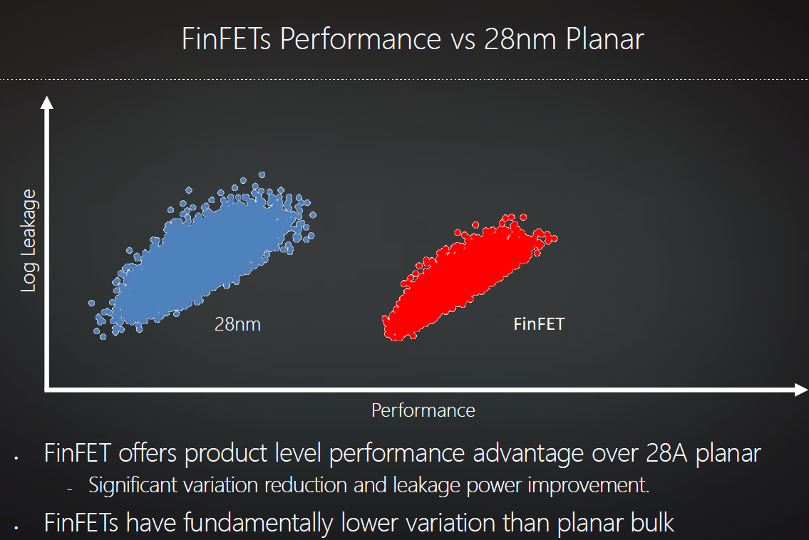
AMD's new microarchitecture is called Polaris. A chunk of data about her appeared on January 4. Polaris supports HDMI 2.0a (output up to 4K 60 FPS), DisplayPort 1.3 (output up to 8K 60 FPS), 4K h.265 (HEVC) encoding and decoding. AMD will use the 14 nm FinFET process technology. Relative to the 28-nm process technology, better speeds, less leakage currents, less variation in the performance of the elements will be achieved.
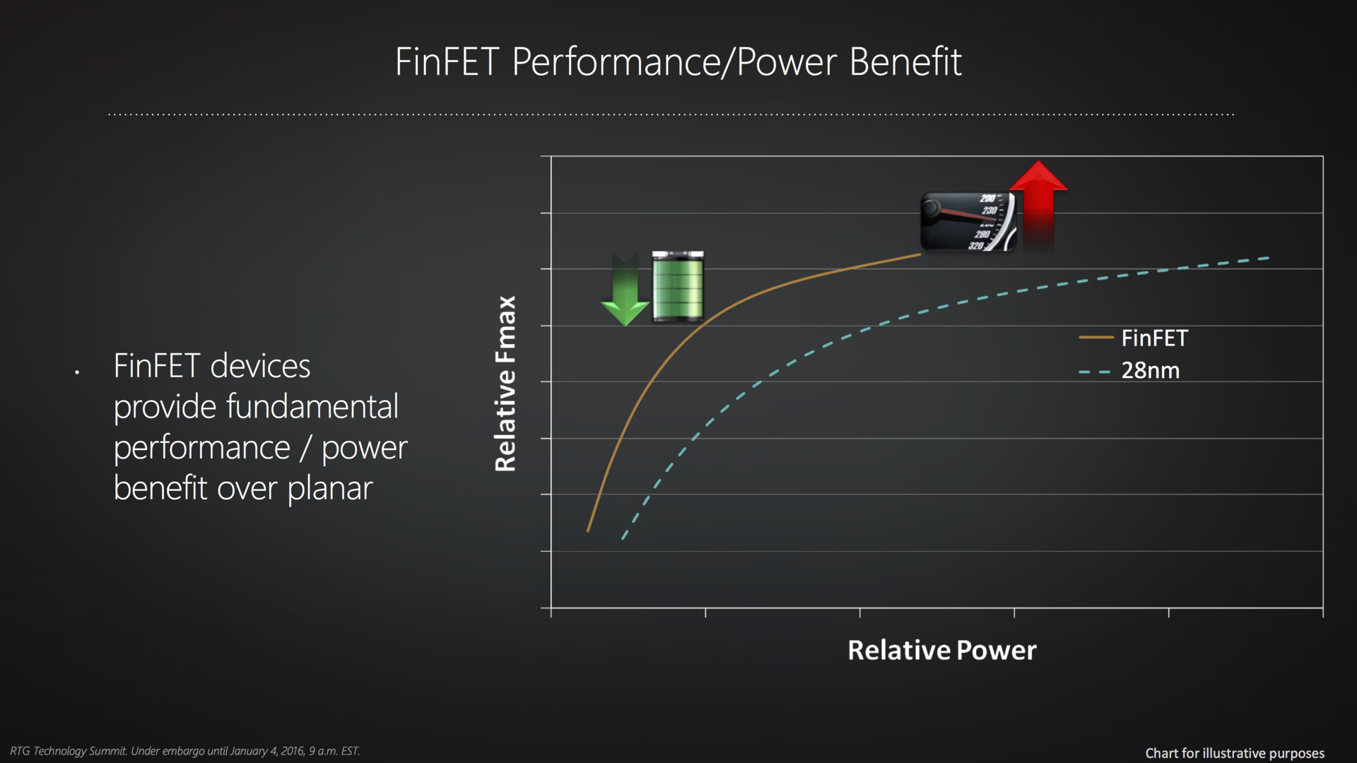
AMD will find the ideal point to improve energy efficiency by delivering performance gains through architectural changes. As the graph below shows, the new process technology provides a good reduction in energy consumption at the same frequency, but not so large a space for increasing productivity. AMD focuses on performance per watt, not performance per se. This will allow you to achieve a console level of graphics even in compact laptops. However, this does not mean that Polaris will not continue to increase productivity. Just to achieve new indicators will be involved changes in architecture, rather than a dumb increase in frequencies. AMD did not provide much information, but it follows from what has been provided that many blocks of graphic chips have been recycled. Polaris is the fourth generation
Graphics Core Next , so the architecture inherits the same principles. Each computing unit contains 4 SIMD blocks, which in turn contain vector computing blocks. It is not known whether the Greens will continue to use GDDR5 in budget products. Micron has made several announcements about GDDR5X technology, which bodes about twice the speed of GDDR5. However, GGDR5X is Micron's proprietary technology, and deliveries are possible closer to the end of 2016. In turn, the Reds are already claiming that GDDR5 will remain in products that focus on low power consumption or average performance. What specific models will contain the "old" type of memory, AMD has not yet said.

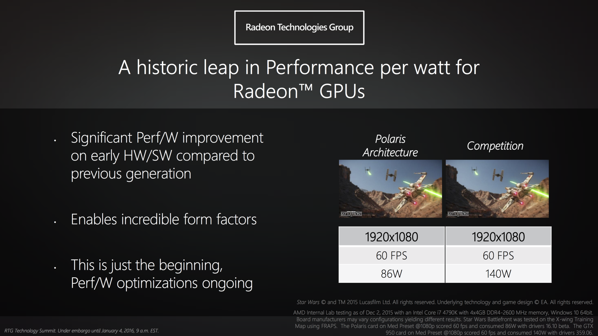
AMD demonstrated a prototype of such an inexpensive Polaris microarchitecture video accelerator with GDDR5 memory instead of HBM. It was compared with an unnamed GTX 950 sample. Energy consumption was recorded in Star Wars Battlefront in 1920 × 1080 resolution. It is difficult to draw any conclusions in this test, where the frame rate was limited to 60 fps, but the Polaris card consumed almost 40% less energy: around 85 watts versus 140.
In the second minute, talking heads are replaced by a demonstration of this test.
AMD currently points to mid-2016 as the release date for Polaris video cards.
Based on ExtremeTech ( 1 , 2 , 3 , 4 ) and Ars Technica .