An inside look at a modern domestic microelectronics plant and not only
In February, a new plant for the production of sensors and systems was opened in Kursk. They opened it pompously: a red ribbon, first persons, all things ... A couple of weeks after the opening I was sent there for work and I took this opportunity to take pictures of what was inside. I will share my impressions.
Details below (many photos).
The plant is located on the outskirts of the city, consists of seven huge red hangars, in appearance you can not even say that inside the production.
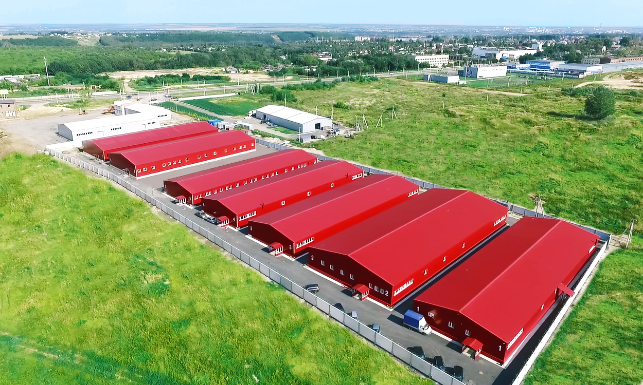
So far, only the 1st stage has been opened, so not all buildings are working yet, only 1,2, 6 and 7. Let's go in order.
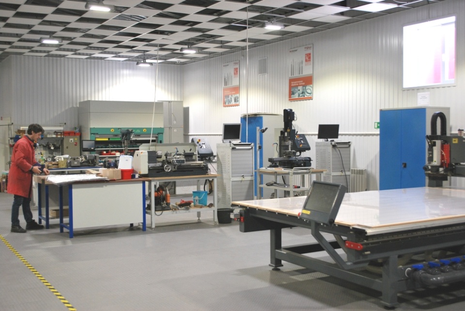
In the first building they have a “locksmith”, they work here mainly with metal, assemble cabinets, lamps, etc.
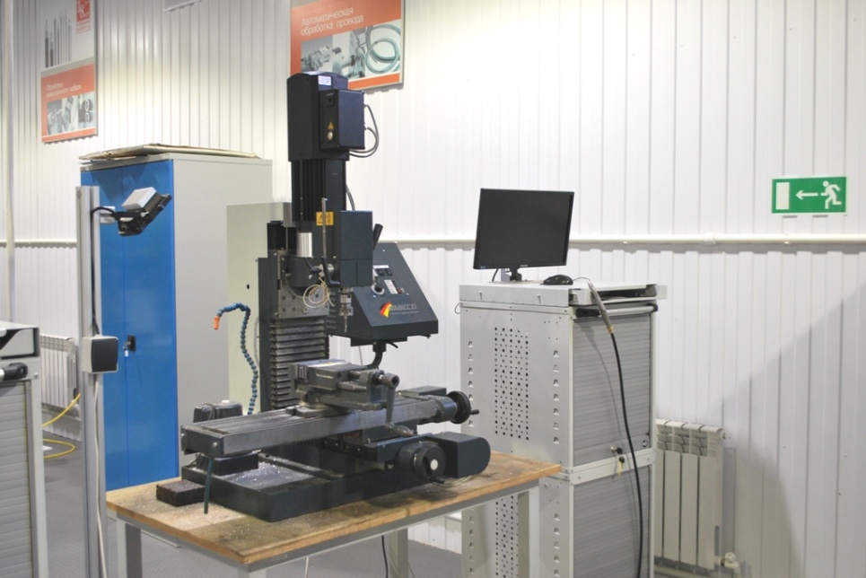
Milling Machine
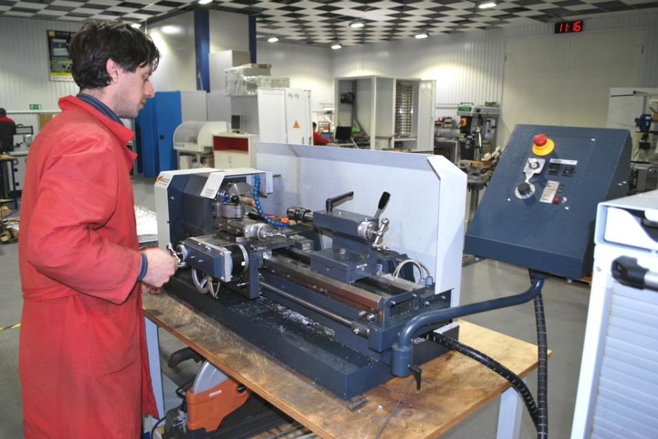
Lathe
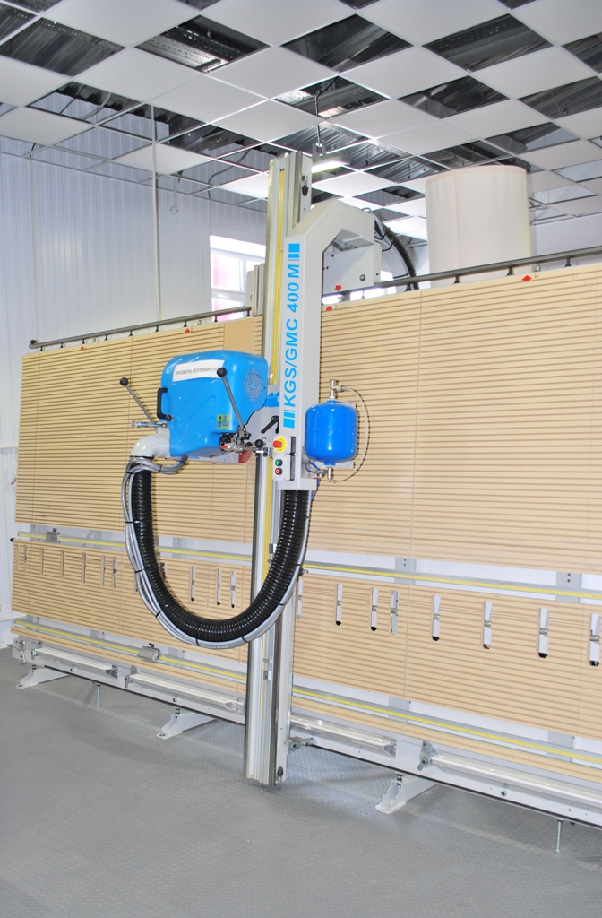
Panel saw machine. For those who do not know: a large format sheet (for example, chipboard) is taken, mounted vertically and cut into small pieces.
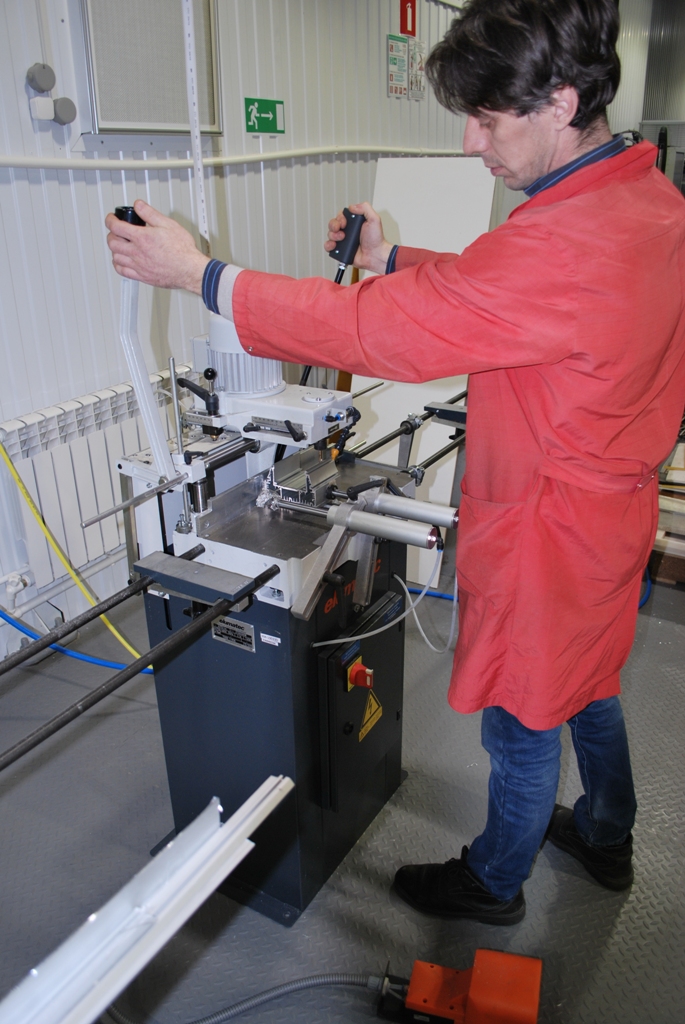
Copy milling machine (works according to the template)
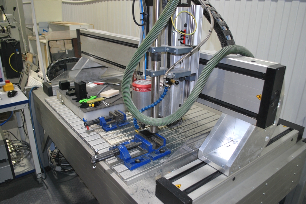
Another kind of milling machine
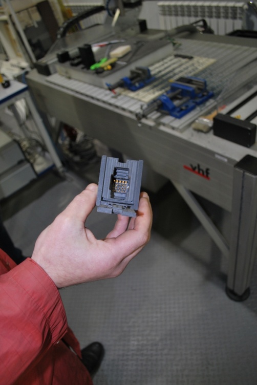
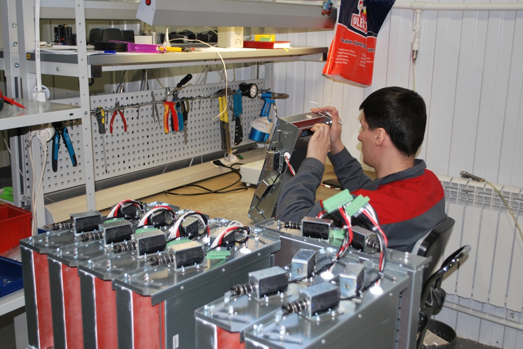
These are the things they collect here
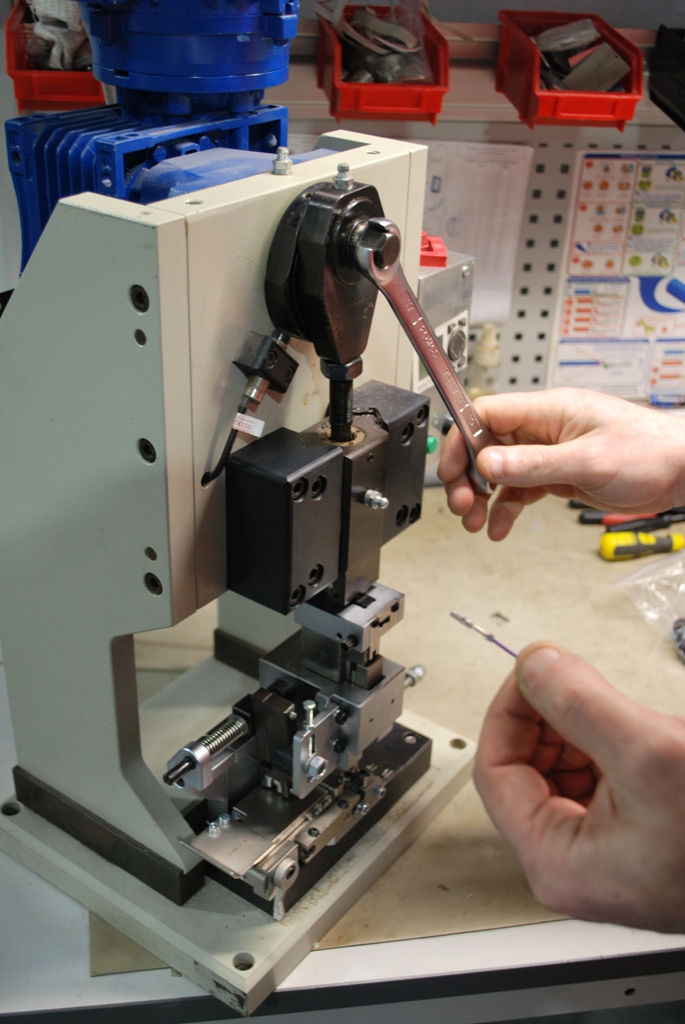
This is an assembly of applicators for pressure testing of wire.
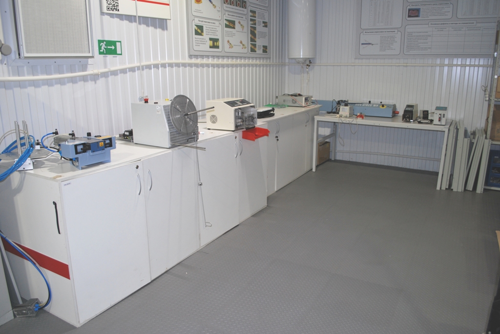
Equipment for cable processing.
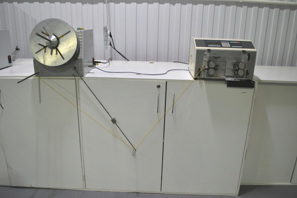
Automated process of cutting and stripping.
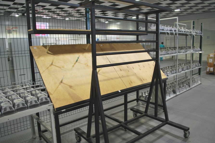
Table for layout of a bundle. By the way, by the way, there are LED lamp
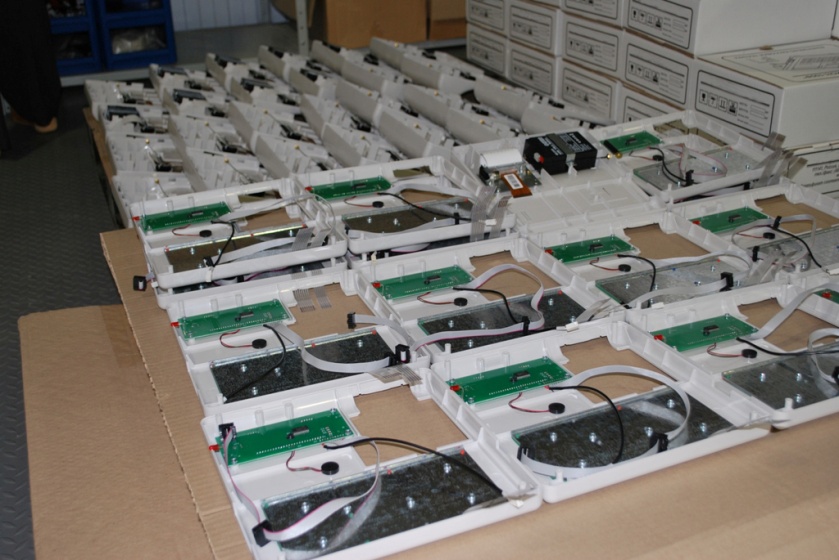
housings. Cash register housings.
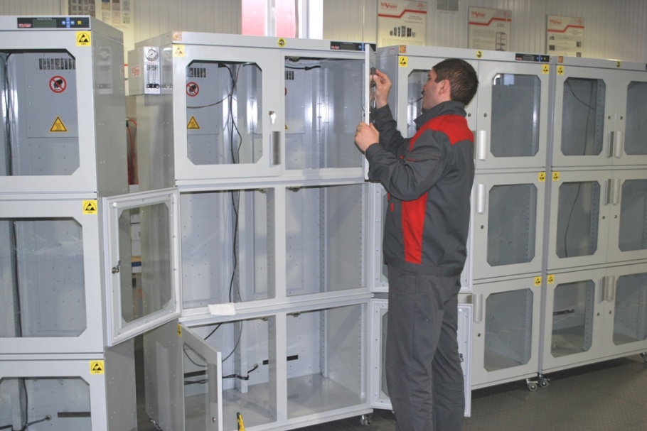
Assembly of dry storage cabinets.
This is a “stuffing” for cabinets, it is made here, only in another building.
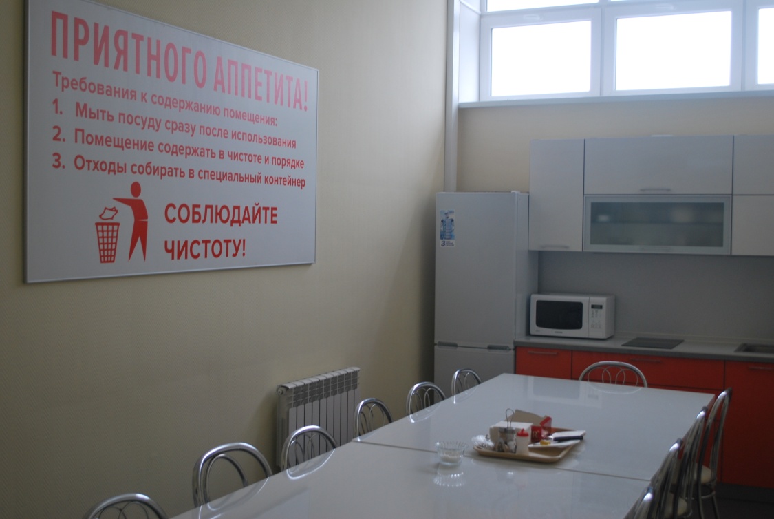
Dining room for employees
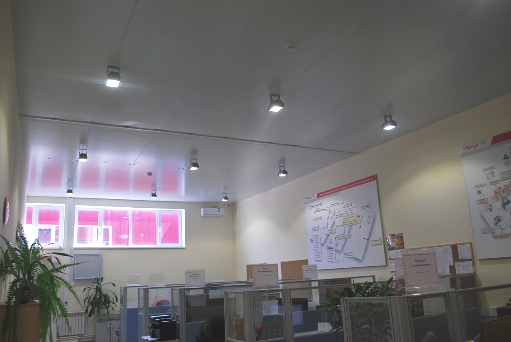
Office rooms
In this building, I didn’t notice anything interesting, we go further.
In the second case, the printed circuit boards are assembled.
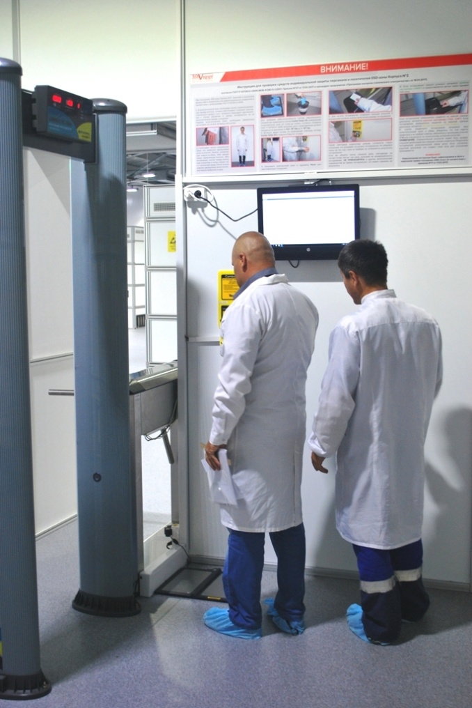
At the entrance is the ESD control post. You can only enter in antistatic clothing and shoes.
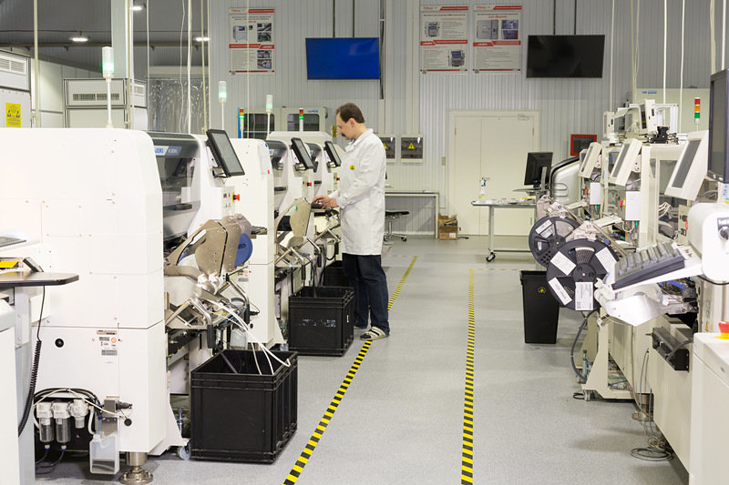
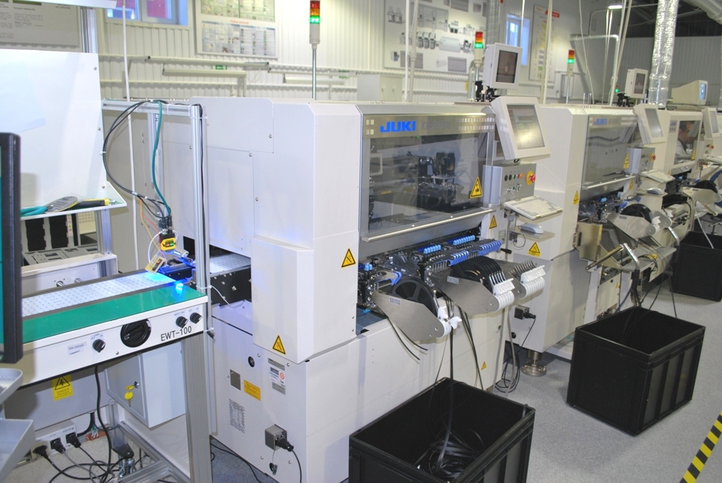
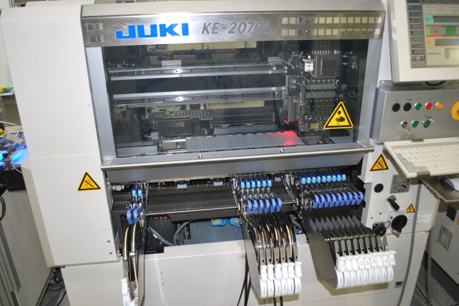
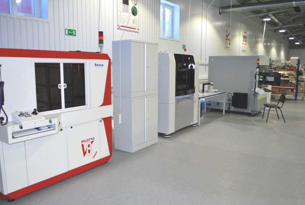
SMT installation lines
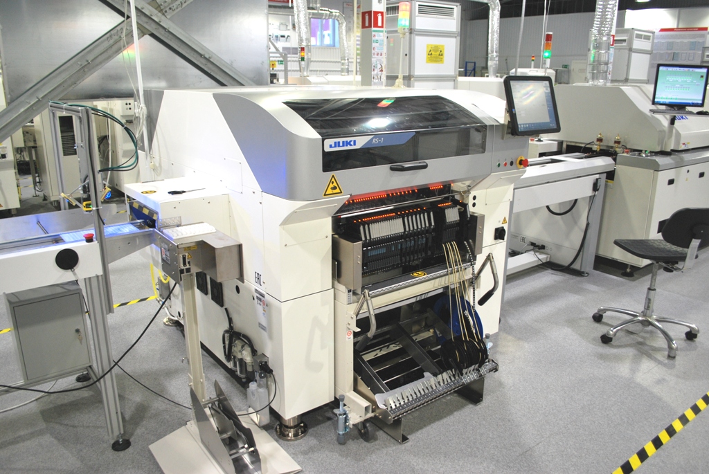
Component installers
There is only one installer on the third line, but they say they are the fastest.
Monitors are hanging on the wall: you can see how many boards have already been made, and how many are left.
Barcodes of the boards are scanned at the inlet and outlet of the line.
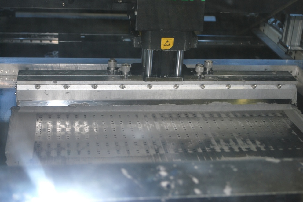
Soldering paste is applied through a stencil.
Installing components.
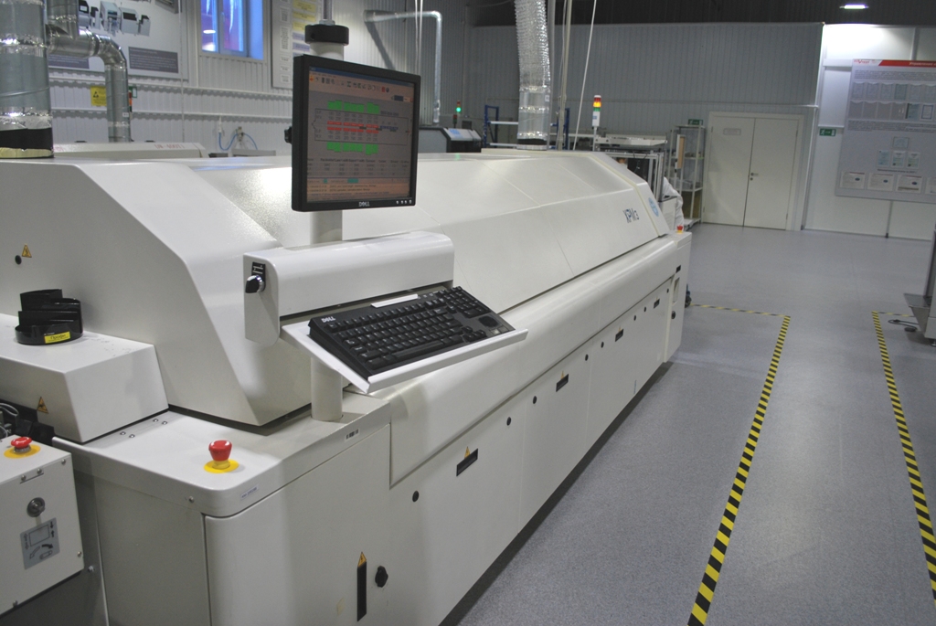
Convection oven.
At the outlet, the boards go to the unloader and then go to the control.
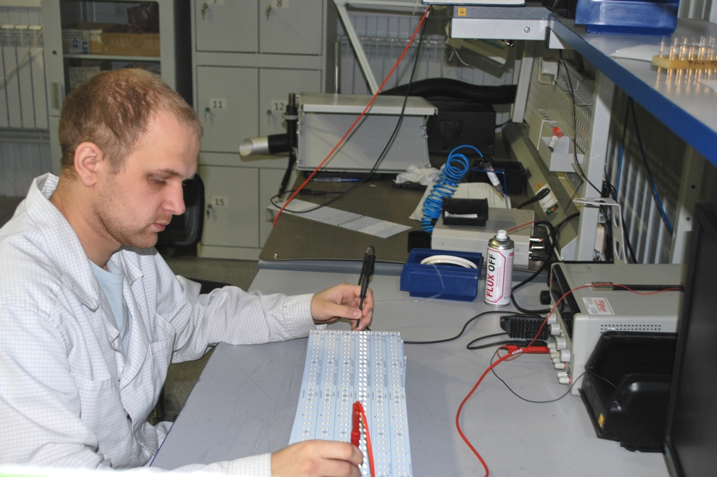
Functional control of LED rulers
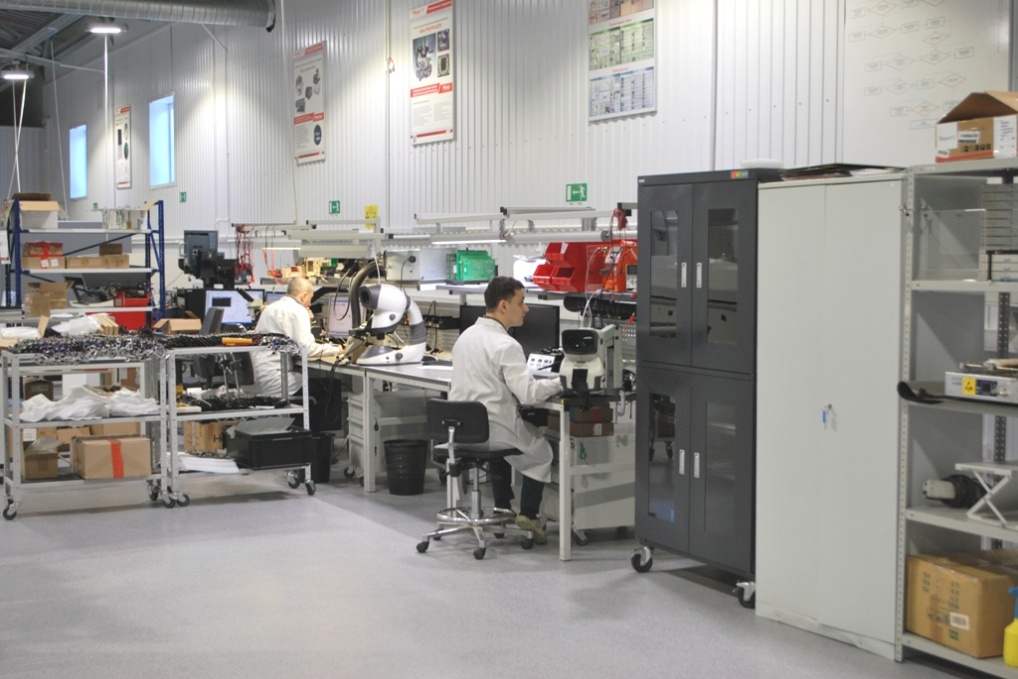
Manual component mounting area
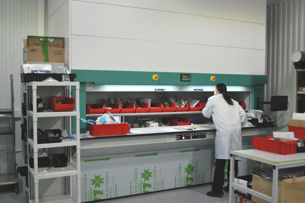
Components are stored in such cabinets, inside there is a carousel-based mechanism
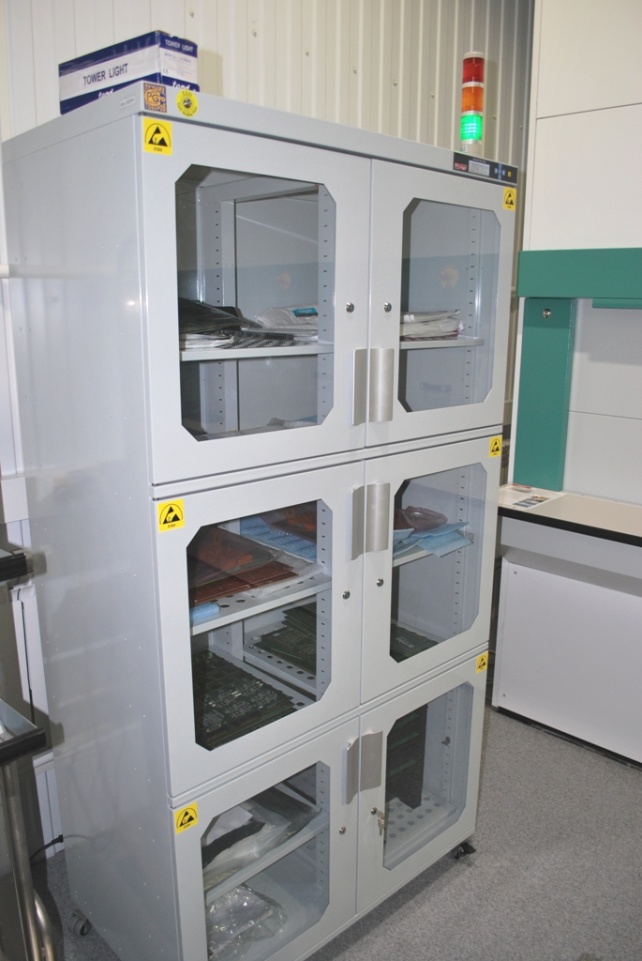
Sensitive components are stored separately - in dry storage cabinets.
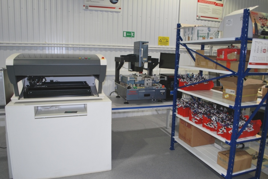
On this site, they check the quality of the solder and look for defects.
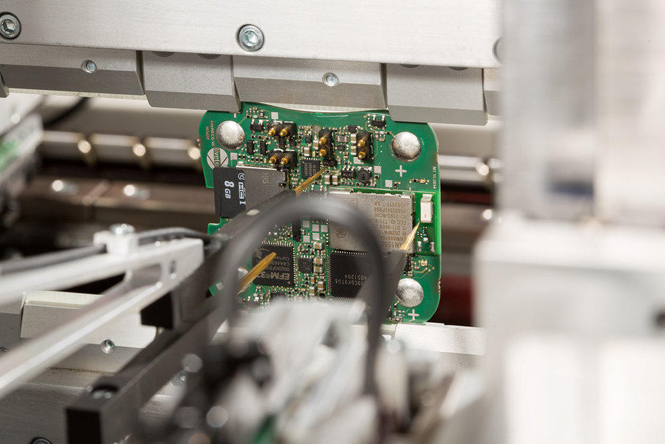
This is how the board is tested using “flying” probes.
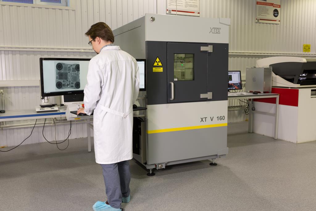
There is an X-ray next to it, which looks at the quality of the soldered joints, which cannot be evaluated from the outside (like BGA , for example)
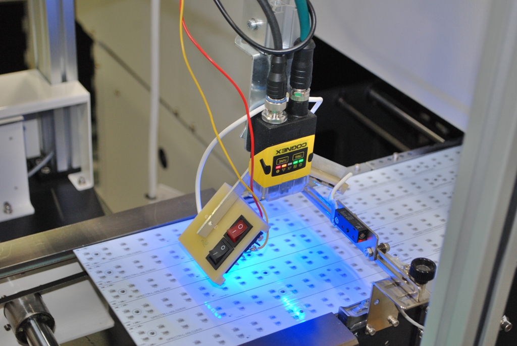
Everything that can be seen from the outside is viewed through an optical inspection system.
There is also a Center for Non-Destructive Testing Technologies at the plant. It is located in the sixth building. Let's go there.
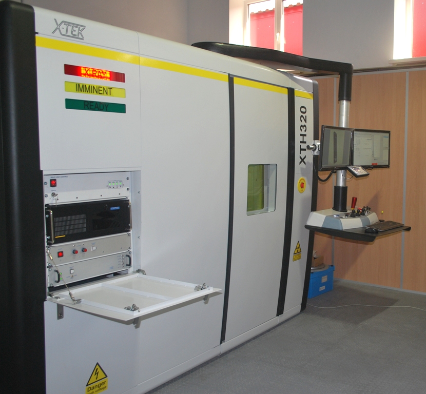
This colossus is an industrial Nikon XT H 320 PentaSource tomograph, it is the only one in Russia. With it, you can "look" inside the product without disassembling the case.
In addition to the tomograph there is still a bunch of all kinds of microscopes, but this is not so interesting.
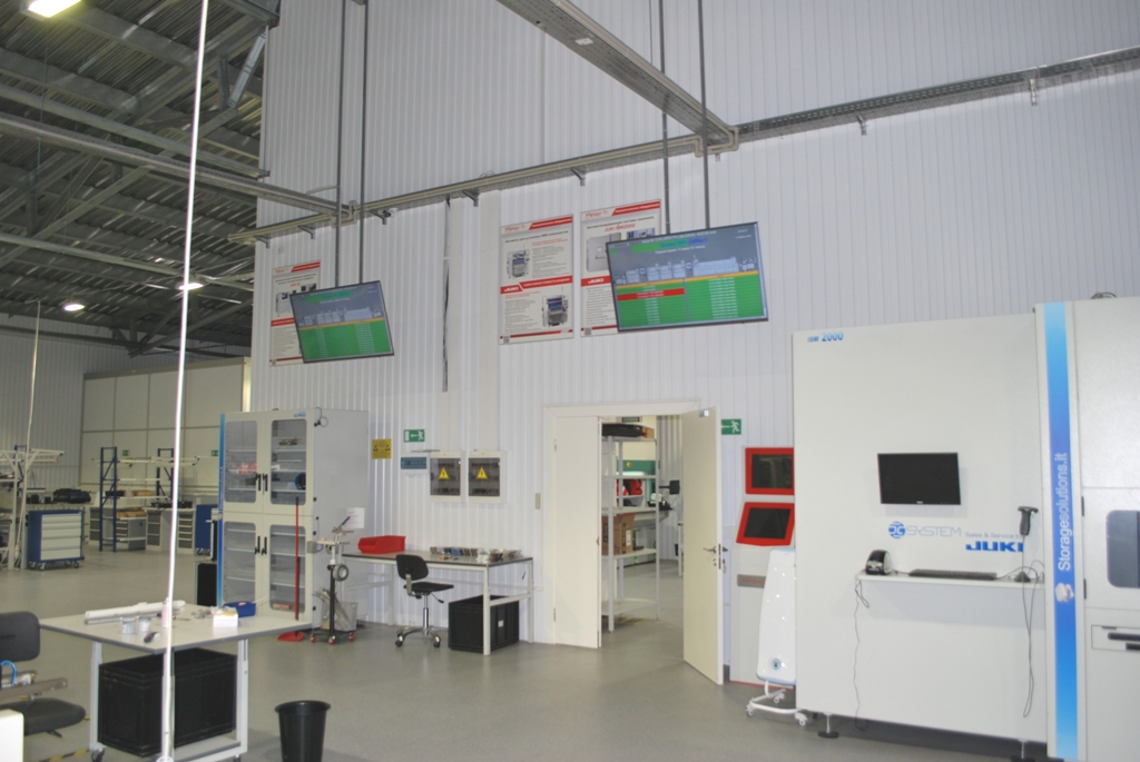
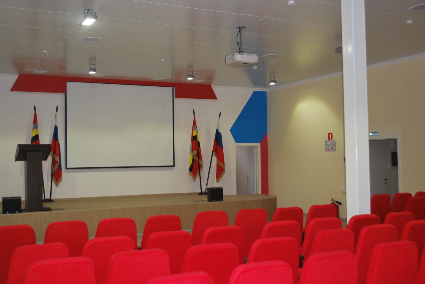
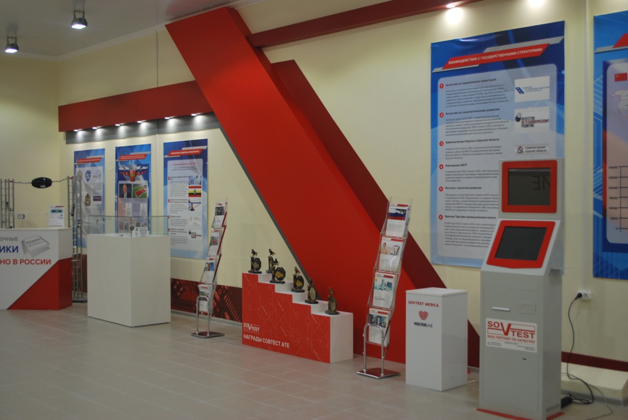
In the last - 7th building - there is a demo hall, a small dining room and a conference room.
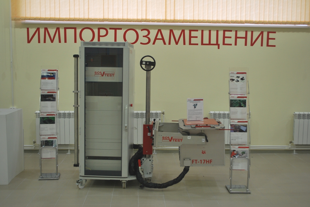
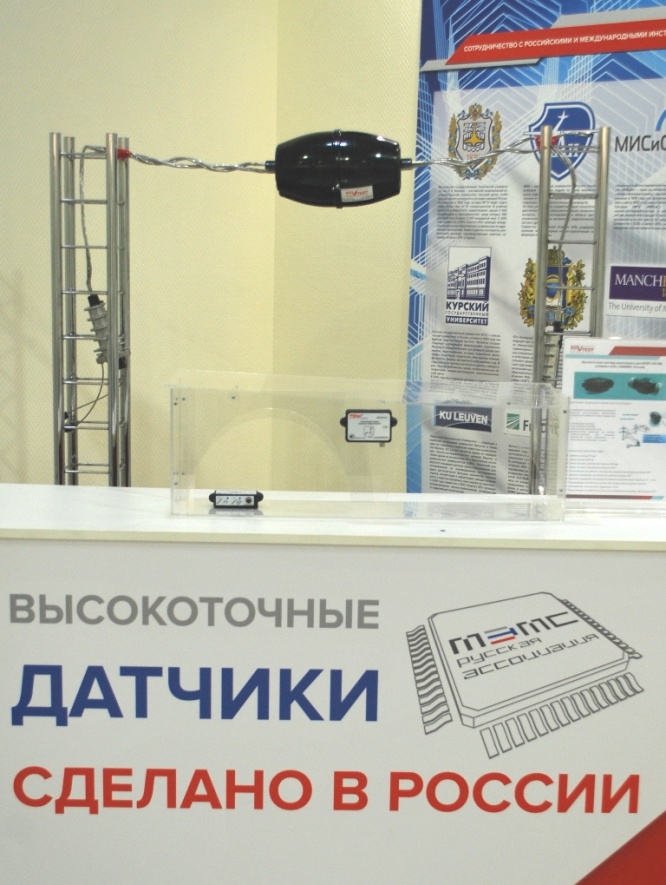
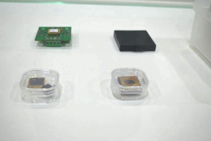
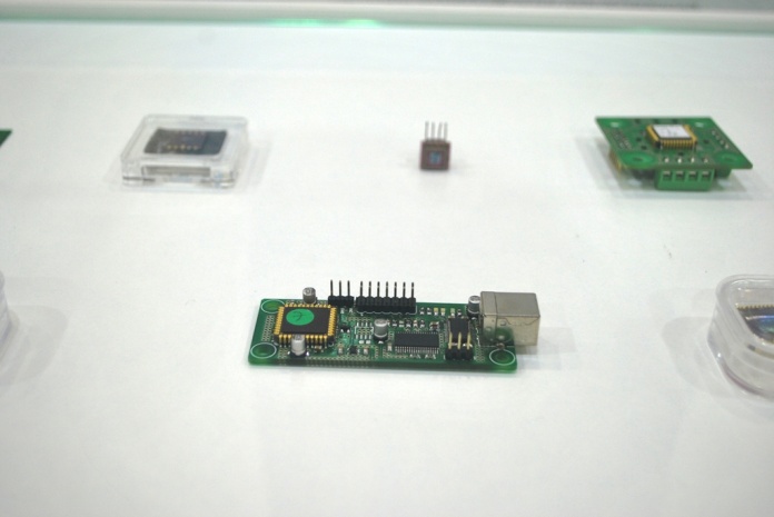
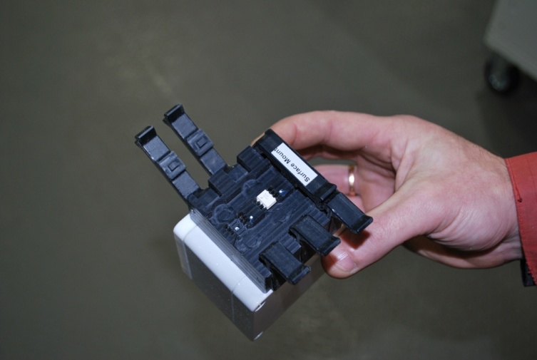
And this, in fact, is the very sensors that are going to be released here. But for this, you must first open the 2nd and 3rd stage of the plant. So far, only prototypes can be seen.
In general, the impressions of the plant remained the most optimistic - the production is lively, modern. There are not so many people, apparently, due to the fact that most processes are automated. It is interesting, of course, to see what will happen in the remaining buildings. But first let them finish. So, most likely, to be continued ...
Details below (many photos).
The plant is located on the outskirts of the city, consists of seven huge red hangars, in appearance you can not even say that inside the production.
So far, only the 1st stage has been opened, so not all buildings are working yet, only 1,2, 6 and 7. Let's go in order.
In the first building they have a “locksmith”, they work here mainly with metal, assemble cabinets, lamps, etc.
Milling Machine
Lathe
Panel saw machine. For those who do not know: a large format sheet (for example, chipboard) is taken, mounted vertically and cut into small pieces.
Copy milling machine (works according to the template)
Another kind of milling machine
These are the things they collect here
This is an assembly of applicators for pressure testing of wire.
Equipment for cable processing.
Automated process of cutting and stripping.
Table for layout of a bundle. By the way, by the way, there are LED lamp
housings. Cash register housings.
Assembly of dry storage cabinets.
This is a “stuffing” for cabinets, it is made here, only in another building.
Dining room for employees
Office rooms
In this building, I didn’t notice anything interesting, we go further.
In the second case, the printed circuit boards are assembled.
At the entrance is the ESD control post. You can only enter in antistatic clothing and shoes.
SMT installation lines
Component installers
There is only one installer on the third line, but they say they are the fastest.
Monitors are hanging on the wall: you can see how many boards have already been made, and how many are left.
Barcodes of the boards are scanned at the inlet and outlet of the line.
Soldering paste is applied through a stencil.
Installing components.
Convection oven.
At the outlet, the boards go to the unloader and then go to the control.
Functional control of LED rulers
Manual component mounting area
Components are stored in such cabinets, inside there is a carousel-based mechanism
Sensitive components are stored separately - in dry storage cabinets.
On this site, they check the quality of the solder and look for defects.
This is how the board is tested using “flying” probes.
There is an X-ray next to it, which looks at the quality of the soldered joints, which cannot be evaluated from the outside (like BGA , for example)
Everything that can be seen from the outside is viewed through an optical inspection system.
There is also a Center for Non-Destructive Testing Technologies at the plant. It is located in the sixth building. Let's go there.
This colossus is an industrial Nikon XT H 320 PentaSource tomograph, it is the only one in Russia. With it, you can "look" inside the product without disassembling the case.
In addition to the tomograph there is still a bunch of all kinds of microscopes, but this is not so interesting.
In the last - 7th building - there is a demo hall, a small dining room and a conference room.
And this, in fact, is the very sensors that are going to be released here. But for this, you must first open the 2nd and 3rd stage of the plant. So far, only prototypes can be seen.
In general, the impressions of the plant remained the most optimistic - the production is lively, modern. There are not so many people, apparently, due to the fact that most processes are automated. It is interesting, of course, to see what will happen in the remaining buildings. But first let them finish. So, most likely, to be continued ...