JTAG to every home: full USB access
Positive Technologies researchers have activated hardware debugging (JTAG) for the Intel Management Engine, which allows full access to all PCH devices (Platform Controller Hub) using Intel DCI technology (via USB). We plan to share the details at one of the upcoming conferences. And how to activate this interface, but for the main processor, we will tell below.
No one is safe from mistakes. This statement also applies to low-level programming, where such familiar means as debugging printing or software debugging at some point may not be enough. To solve this problem, hardware developers use the so-called in-circuit emulators or a special JTAG debugging interface if it is present on the target platform (IEEE1149.1 [1]). These debugging mechanisms appeared in the 80s of the last century [2]. Over time, chip manufacturers have expanded the capabilities of these interfaces. Thanks to this, the developers were able to get detailed information about energy consumption, find bottlenecks in high-performance algorithms and got many other features.
For security researchers, debugging hardware is also of interest. They allow you to get low-level access to the system bypassing the basic means of security, to study the behavior of the target platform and its undocumented features. Obviously, such opportunities turned out to be attractive for special services [3].
For a long time, only a limited number of people had access to these technologies for Intel processors, which was associated with the need to use expensive specialized equipment. But with the release of processors from the Skylake family, the situation changed dramatically: debugging mechanisms were built into PCH [4], which allows ordinary users to use such a powerful tool - including cybercriminals, who can thus gain complete control over the processor. For security reasons, these mechanisms are not activated by default, but in this article we will show that they can be made to work on equipment that is available in ordinary computer stores.
1. From in-circuit emulator to JTAG
Initially, the in-circuit emulator (ICE) for Intel 80286 processors was a separate computer (the “big blue box” [5]), which included a keyboard and a monitor. ICE connected instead of the processor of the debugged system and emulated its behavior. Such an emulator allowed you to set breakpoints, change memory and processor registers, and write and read.
Later, Intel introduced the new I2ICE hardware debugger (Fig. 1), which no longer replaced a regular processor. Using special adapters, the user was connected to a debugged system, and such a hardware debugger used a standard serial port at 9600 Baud to communicate with the host machine [5].
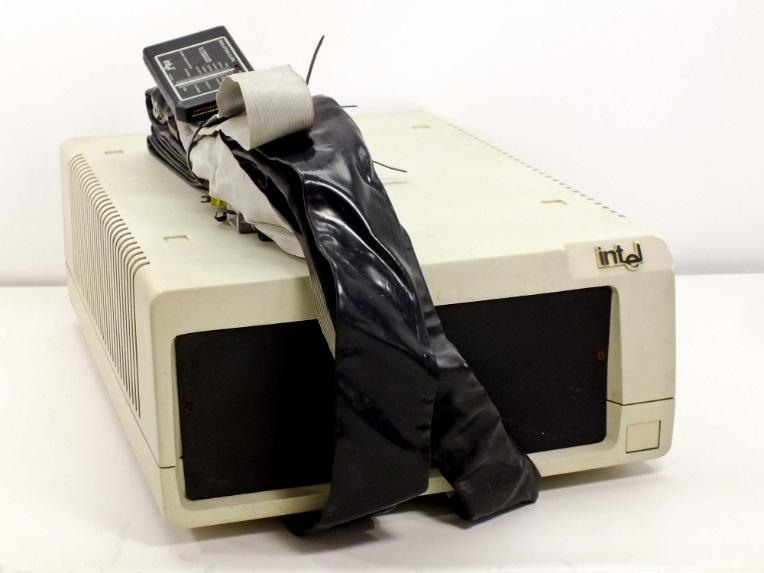
Fig. 1. Intel I2ICE is one of the first in-circuit debuggers for Intel 80386 processors (recycledgoods.com/intel-series-iv-emul-system-iii514b.html)
As technology develops and clock speeds increase, Intel refuses to develop separate full-featured debugging tools and partially transfers it inside the processor, in the form of a special, undocumented ICE-mode (which, according to the principles of operation, was very similar to another mode - System Management Mode (SMM), some developers of that time had a strong belief that SMM is nothing more than documented and extended ICE-mode [ 6]). In turn, the general standardization of debugging mechanisms in the electronics industry leads to the fact that some Intel 80486 processors support the IEEE1149.1 (JTAG) test interface [7].
The Joint Test Action Group (JTAG) is actually the name of the working group that developed the Standard Test Access Port Port and Boundary-Scan Architecture (IEEE1149.1 [1]). It allows you to use standard testing and debugging equipment for a wide class of devices. Over time, the abbreviation JTAG became associated with the IEEE1149 standard. In modern microcircuits, it is widely used in industry and is used for testing, flashing, debugging, and output control of microcircuits in production. Physically, a JTAG is four or five leased lines that form the Test Access Port (TAP). The standard provides for the combination of devices in a chain, allowing access to each connected device (Fig. 2).
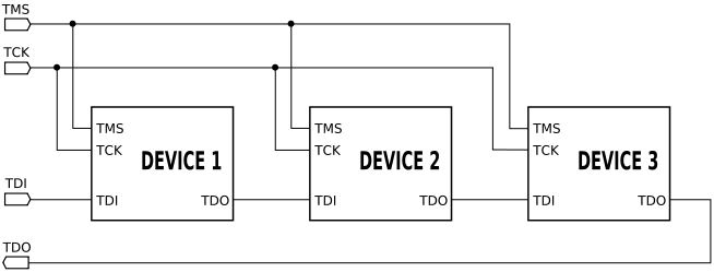
Fig. 2. Combining debugged devices in a JTAG chain
Often, hardware developers expand the basic functionality of JTAG, introducing new features; Intel processors were no exception in this sense, starting with Pentium there is a cheaper and more powerful version of an external debugger that uses a special probe mode.
2. Probe debugging mode
The probe mode is another undocumented mode of Intel processors. It is used for diagnostics and debugging. It cannot be activated without access to the processor JTAG registers. In probe mode, the processor can change memory, write and read from I / O ports. In this mode, the normal execution of instructions is interrupted and the processor goes into idle mode, waiting for commands via the JTAG interface. This behavior fundamentally distinguishes this mechanism from ICE-mode, when instructions on the processor continued to be executed. When entering probe mode, the prefetching and decoding of the commands stops. Commands from JTAG for modification or reading go directly to the execution units of the processor, thereby bypassing the stages of prefetching and decoding [8],
Probe mode is implemented as a JTAG extension with the addition of several registers and additional signals R / S #, PRDY (for more details on how probe mode is implemented, see [8], [9]). Third-party companies, along with Intel, release JTAG adapters for x86 processors that support this extension, but we will only look at original debugging hardware.
3. Modern Intel
processor hardware and technology debugging Modern Intel processors provide JTAG through three interfaces:
- USB3 Hosting DCI (USB-Debug cable) - through a regular DbC cable;
- BSSB Hosting DCI (Intel SVT Closed Chassis Adapter) - through a specialized adapter (Fig. 5).
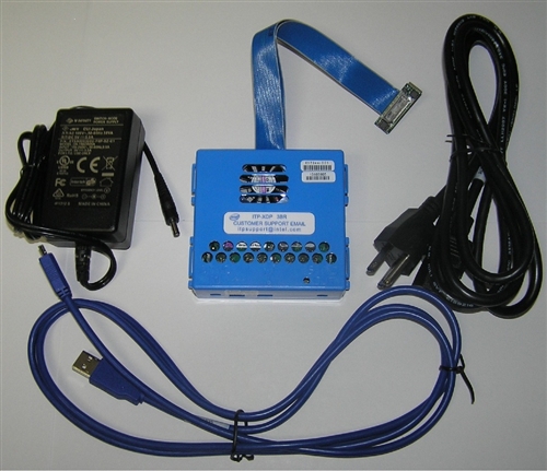
Fig. 3. ITP-XDP
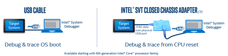
Fig. 4. DCI connection types
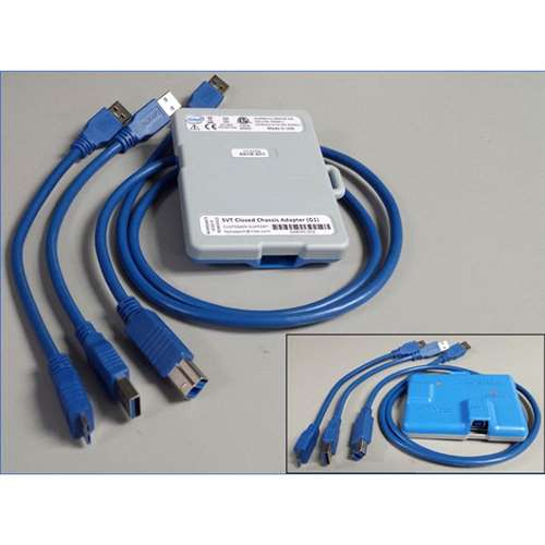
Figure 5. Intel SVT Closed Chassis Adapter
The Intel ITP-XDP interface has a closed protocol, requires a dedicated connector on the board and specialized Intel System Studio software (a trial version is available on the manufacturer’s website). The disadvantages also include the high price (about 3,000 US dollars) and the need to sign documents on non-disclosure of information (Corporate Non-Disclosure Agreement) [10]. The high price and CNDA make this debugger inaccessible to the average developer or home use.
However, starting with the processors of the Skylake family, Intel introduced the Direct Connect Interface (DCI) technology, its rather superficial description can be found in the documentation [4]. This technology aims to simplify the development of mobile devices, which implies its drawback: it can be activated without any hardware modifications (if there are JTAG lines between PCH and CPU). It is also worth noting that the connection using the Intel SVT adapter uses USB 3.0 lines, but implements its own protocol, which allows you to work with the target system in deep sleep modes. Unfortunately, the SVT adapter at its relatively low price (390 US dollars) is also available for purchase only after signing the CNDA.
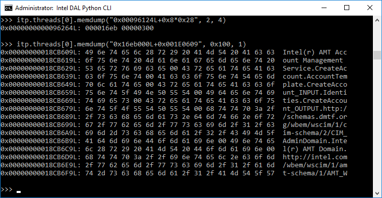
The most interesting option for the average programmer, which does not require signing any documents before use, is USB3 Hosting DCI. It presents the JTAG interface through a regular USB 3.0 debugging cable. When DCI is activated on the target system, the USB 3.0 port enters slave mode and starts receiving commands from the host system.
One of the important questions regarding USB 3.0 DbC DCI Hosting is whether it is possible to connect to DCI through any external USB 3.0 port - or does it require a debug port that is available only on special development boards. This issue should be considered in more detail.
There is a confusion in the environment of system developers, caused by the fact that debugging via USB itself has appeared a long time ago (since the times of USB 2.0) and is currently used by many developers to programmatically debug operating system kernels and UEFI applications. However, software debugging via USB (in windbg, UEFI debug agent, etc.) has nothing to do with hardware debugging mechanisms through JTAG, except for the transport itself. The USB 2.0 Bus Controller Specification (EHCI, Enhanced Host Controller Interface) provides a special mechanism called the Debug Port (PCI capability), which allows interaction between the server (software or hardware) on the debugged machine and the client on the host. In particular, the Windows kernel supports debugging via the EHCI Debug Port (in this case, you need a USB 2.0 debugging cable, with integrated USB 2.0 device). At the same time, indeed, not every external USB 2.0 port could work as a Debug Port, but this feature was assigned to certain ports that might not have been brought out. It all depended on the equipment manufacturer. Therefore, the developers specifically looked for equipment with Debug Port brought out for USB debugging. Thus, the Debug Port is an attribute of the USB port.
However, the situation has completely changed with the advent of USB 3.0 and the controller specification for this XHCI bus (eXtended Host Controller Interface). This specification also supports USB debugging, but it has undergone significant development and has become known as USB Debug Capability (DbC). According to XHCI, DbC is not a port attribute, but a property of a specific XHCI controller. That is, if this XHCI controller supports DbC, then USB 3.0 debugging will be available on any (including external) USB 3.0 port. In this case, DbC will automatically select the first port to which a client performing USB 3.0 transactions is connected with a debug cable.
It is important to note here that the first XHCI controllers did not support DbC, so USB debugging was not possible on systems with such controllers. However, in PCH version 100 and later (for Skylake), Intel has built its own XHCI controller that supports DbC. Intel DCI technology (which appeared since the Skylake processors) uses USB 3.0 DbС as a transport for connecting a JTAG client. It does not use USB 2.0 Debug Port.
Thus, through any USB 3.0 port, you can connect to DCI and perform JTAG debugging.
How can you activate this debugging interface? We found three ways:
1. Activation via EFI Human Interface Infrastructure
EFI Human Interface Infrastructure is a special mechanism that allows you to create a user interface in UEFI, process and control user input. If you look at the structure of modern UEFI BIOS, you can find in them a lot of hidden options that are not accessible to the user, but are processed. Our first method is based on this. EFI HII defines default values for all options, including hidden ones. Once you find an option related to DCI, you can activate it for the default setting, and then, after setting the BIOS to factory settings, activate DCI. These settings can be edited using the AMI BIOS Configuration Program 5.0 utility. The edited image is programmed in the SPI-flash programmer or through the standard BIOS firmware mechanism, if access permissions allow.
However, this method has a drawback: the system will not boot if Boot Guard is activated, since the utility modifies the EFI module.
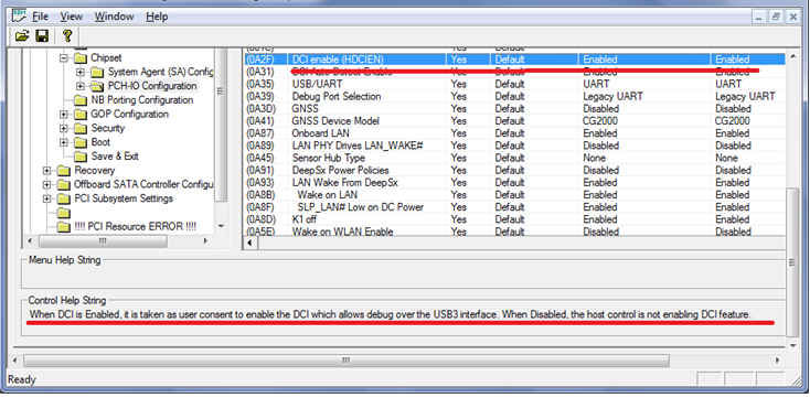
2. Activation via the Flash Descriptor Region
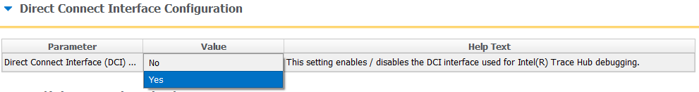 DCI can also be activated by setting special bits of the PCH configuration - either manually (they are in the Flash Descriptor Region), or using the Flash Image Tool. This method works even when Boot Guard is enabled.
3. Activation via a P2SB device
In the end, you can try to act directly - through a P2SB device. In the documentation for different generations of PCH, you can find a special index and register, using which you can activate DCI on the fly if the BIOS did not block changing the DCI setting.
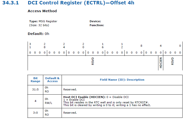
This method is a vulnerability, because if the BIOS does not block writing to the ECTRL register, then due to the nature of the operation (the ability to save the configuration between reboots after turning off the power) it allows DCI to be activated once, and then use the JTAG interface as a hardware backdoor to the system ( for example, turn off the lock screen).
We conducted a study [12], as a result of which it turned out that the largest manufacturers of motherboards do not lock this register, which allows you to activate DCI and use this mechanism, for example, to overwrite the BIOS bypassing all security features, including digital signature verification.
The presence of debugging mechanisms in modern Intel processors makes it easier to develop UEFI modules, operating systems, and hypervisors. Security researchers get a low-level mechanism of privileged access to hardware, which can be used to search for malicious software, research undocumented hardware capabilities or drivers of specific equipment. But, like any debugging mechanism, DCI can be used by attackers to unauthorized access to data.
As protection against such attacks, we recommend activating Boot Guard, checking the DCI activation bit and debugging in the IA32_DEBUG_INTERFACE register (in this case, DCI can work, but it is no longer possible to stop execution, so there is no way to access memory and registers).
Authors: Maxim Goryachiy, Mark Ermolov.
1.149.1-1990 - IEEE Standard Test Access Port and Boundary-Scan Architecture.
2. www.jtag.com/en/content/about-jtag-technologies
3. resources.infosecinstitute.com/close-look-nsa-monitor-catalog-server-hacking
4. 6th Generation Intel Core Processor I / O Datasheet. Vol. 2.
5. In-Circuit Emulation, Robert R. Collins (rcollins.org/ddj/Jul97).
6. Intel's System Management Mode by Robert R. Collins // Dr. Dobb's Journal. January 1997.
7. Guk M. Intel processors from 8086 to Pentium II - St. Petersburg: Peter, 1998.
8. Overview of Pentium Probe Mode by Robert R. Collins (rcollins.org/articles/probemd/ProbeMode.html).
9. Guk M. Processors Pentium II, Pentium Pro and simply Pentium - St. Petersburg: Peter, 1999.
10. www-ssl.intel.com/content/www/us/en/forms/design/registration-privileged.html
11. www.asset-intertech.com/products/jtag-interposers-and-arium-jtag-adapters
12. habrahabr.ru/company/pt/blog/321440
No one is safe from mistakes. This statement also applies to low-level programming, where such familiar means as debugging printing or software debugging at some point may not be enough. To solve this problem, hardware developers use the so-called in-circuit emulators or a special JTAG debugging interface if it is present on the target platform (IEEE1149.1 [1]). These debugging mechanisms appeared in the 80s of the last century [2]. Over time, chip manufacturers have expanded the capabilities of these interfaces. Thanks to this, the developers were able to get detailed information about energy consumption, find bottlenecks in high-performance algorithms and got many other features.
For security researchers, debugging hardware is also of interest. They allow you to get low-level access to the system bypassing the basic means of security, to study the behavior of the target platform and its undocumented features. Obviously, such opportunities turned out to be attractive for special services [3].
For a long time, only a limited number of people had access to these technologies for Intel processors, which was associated with the need to use expensive specialized equipment. But with the release of processors from the Skylake family, the situation changed dramatically: debugging mechanisms were built into PCH [4], which allows ordinary users to use such a powerful tool - including cybercriminals, who can thus gain complete control over the processor. For security reasons, these mechanisms are not activated by default, but in this article we will show that they can be made to work on equipment that is available in ordinary computer stores.
The evolution of debugging tools on Intel processors
1. From in-circuit emulator to JTAG
Initially, the in-circuit emulator (ICE) for Intel 80286 processors was a separate computer (the “big blue box” [5]), which included a keyboard and a monitor. ICE connected instead of the processor of the debugged system and emulated its behavior. Such an emulator allowed you to set breakpoints, change memory and processor registers, and write and read.
Later, Intel introduced the new I2ICE hardware debugger (Fig. 1), which no longer replaced a regular processor. Using special adapters, the user was connected to a debugged system, and such a hardware debugger used a standard serial port at 9600 Baud to communicate with the host machine [5].
Fig. 1. Intel I2ICE is one of the first in-circuit debuggers for Intel 80386 processors (recycledgoods.com/intel-series-iv-emul-system-iii514b.html)
As technology develops and clock speeds increase, Intel refuses to develop separate full-featured debugging tools and partially transfers it inside the processor, in the form of a special, undocumented ICE-mode (which, according to the principles of operation, was very similar to another mode - System Management Mode (SMM), some developers of that time had a strong belief that SMM is nothing more than documented and extended ICE-mode [ 6]). In turn, the general standardization of debugging mechanisms in the electronics industry leads to the fact that some Intel 80486 processors support the IEEE1149.1 (JTAG) test interface [7].
The Joint Test Action Group (JTAG) is actually the name of the working group that developed the Standard Test Access Port Port and Boundary-Scan Architecture (IEEE1149.1 [1]). It allows you to use standard testing and debugging equipment for a wide class of devices. Over time, the abbreviation JTAG became associated with the IEEE1149 standard. In modern microcircuits, it is widely used in industry and is used for testing, flashing, debugging, and output control of microcircuits in production. Physically, a JTAG is four or five leased lines that form the Test Access Port (TAP). The standard provides for the combination of devices in a chain, allowing access to each connected device (Fig. 2).
Fig. 2. Combining debugged devices in a JTAG chain
Often, hardware developers expand the basic functionality of JTAG, introducing new features; Intel processors were no exception in this sense, starting with Pentium there is a cheaper and more powerful version of an external debugger that uses a special probe mode.
2. Probe debugging mode
The probe mode is another undocumented mode of Intel processors. It is used for diagnostics and debugging. It cannot be activated without access to the processor JTAG registers. In probe mode, the processor can change memory, write and read from I / O ports. In this mode, the normal execution of instructions is interrupted and the processor goes into idle mode, waiting for commands via the JTAG interface. This behavior fundamentally distinguishes this mechanism from ICE-mode, when instructions on the processor continued to be executed. When entering probe mode, the prefetching and decoding of the commands stops. Commands from JTAG for modification or reading go directly to the execution units of the processor, thereby bypassing the stages of prefetching and decoding [8],
Probe mode is implemented as a JTAG extension with the addition of several registers and additional signals R / S #, PRDY (for more details on how probe mode is implemented, see [8], [9]). Third-party companies, along with Intel, release JTAG adapters for x86 processors that support this extension, but we will only look at original debugging hardware.
3. Modern Intel
processor hardware and technology debugging Modern Intel processors provide JTAG through three interfaces:
- Intel In-Target Probe eXtended Debug Port (ITP-XDP) (Fig. 3);
- Intel Direct Connect Interface (DCI) is a specialized technology that provides a JTAG interface through a USB 3.0 port. There are two connection options (Fig. 4):
- USB3 Hosting DCI (USB-Debug cable) - through a regular DbC cable;
- BSSB Hosting DCI (Intel SVT Closed Chassis Adapter) - through a specialized adapter (Fig. 5).
Fig. 3. ITP-XDP
Fig. 4. DCI connection types
Figure 5. Intel SVT Closed Chassis Adapter
The Intel ITP-XDP interface has a closed protocol, requires a dedicated connector on the board and specialized Intel System Studio software (a trial version is available on the manufacturer’s website). The disadvantages also include the high price (about 3,000 US dollars) and the need to sign documents on non-disclosure of information (Corporate Non-Disclosure Agreement) [10]. The high price and CNDA make this debugger inaccessible to the average developer or home use.
However, starting with the processors of the Skylake family, Intel introduced the Direct Connect Interface (DCI) technology, its rather superficial description can be found in the documentation [4]. This technology aims to simplify the development of mobile devices, which implies its drawback: it can be activated without any hardware modifications (if there are JTAG lines between PCH and CPU). It is also worth noting that the connection using the Intel SVT adapter uses USB 3.0 lines, but implements its own protocol, which allows you to work with the target system in deep sleep modes. Unfortunately, the SVT adapter at its relatively low price (390 US dollars) is also available for purchase only after signing the CNDA.
The most interesting option for the average programmer, which does not require signing any documents before use, is USB3 Hosting DCI. It presents the JTAG interface through a regular USB 3.0 debugging cable. When DCI is activated on the target system, the USB 3.0 port enters slave mode and starts receiving commands from the host system.
One of the important questions regarding USB 3.0 DbC DCI Hosting is whether it is possible to connect to DCI through any external USB 3.0 port - or does it require a debug port that is available only on special development boards. This issue should be considered in more detail.
There is a confusion in the environment of system developers, caused by the fact that debugging via USB itself has appeared a long time ago (since the times of USB 2.0) and is currently used by many developers to programmatically debug operating system kernels and UEFI applications. However, software debugging via USB (in windbg, UEFI debug agent, etc.) has nothing to do with hardware debugging mechanisms through JTAG, except for the transport itself. The USB 2.0 Bus Controller Specification (EHCI, Enhanced Host Controller Interface) provides a special mechanism called the Debug Port (PCI capability), which allows interaction between the server (software or hardware) on the debugged machine and the client on the host. In particular, the Windows kernel supports debugging via the EHCI Debug Port (in this case, you need a USB 2.0 debugging cable, with integrated USB 2.0 device). At the same time, indeed, not every external USB 2.0 port could work as a Debug Port, but this feature was assigned to certain ports that might not have been brought out. It all depended on the equipment manufacturer. Therefore, the developers specifically looked for equipment with Debug Port brought out for USB debugging. Thus, the Debug Port is an attribute of the USB port.
However, the situation has completely changed with the advent of USB 3.0 and the controller specification for this XHCI bus (eXtended Host Controller Interface). This specification also supports USB debugging, but it has undergone significant development and has become known as USB Debug Capability (DbC). According to XHCI, DbC is not a port attribute, but a property of a specific XHCI controller. That is, if this XHCI controller supports DbC, then USB 3.0 debugging will be available on any (including external) USB 3.0 port. In this case, DbC will automatically select the first port to which a client performing USB 3.0 transactions is connected with a debug cable.
It is important to note here that the first XHCI controllers did not support DbC, so USB debugging was not possible on systems with such controllers. However, in PCH version 100 and later (for Skylake), Intel has built its own XHCI controller that supports DbC. Intel DCI technology (which appeared since the Skylake processors) uses USB 3.0 DbС as a transport for connecting a JTAG client. It does not use USB 2.0 Debug Port.
Thus, through any USB 3.0 port, you can connect to DCI and perform JTAG debugging.
DCI Activation
How can you activate this debugging interface? We found three ways:
- Via EFI Human Interface Infrastructure
- PCH Strap (Intel Flash Image Tool);
- P2SB device.
1. Activation via EFI Human Interface Infrastructure
EFI Human Interface Infrastructure is a special mechanism that allows you to create a user interface in UEFI, process and control user input. If you look at the structure of modern UEFI BIOS, you can find in them a lot of hidden options that are not accessible to the user, but are processed. Our first method is based on this. EFI HII defines default values for all options, including hidden ones. Once you find an option related to DCI, you can activate it for the default setting, and then, after setting the BIOS to factory settings, activate DCI. These settings can be edited using the AMI BIOS Configuration Program 5.0 utility. The edited image is programmed in the SPI-flash programmer or through the standard BIOS firmware mechanism, if access permissions allow.
However, this method has a drawback: the system will not boot if Boot Guard is activated, since the utility modifies the EFI module.
2. Activation via the Flash Descriptor Region
DCI can also be activated by setting special bits of the PCH configuration - either manually (they are in the Flash Descriptor Region), or using the Flash Image Tool. This method works even when Boot Guard is enabled. 3. Activation via a P2SB device
In the end, you can try to act directly - through a P2SB device. In the documentation for different generations of PCH, you can find a special index and register, using which you can activate DCI on the fly if the BIOS did not block changing the DCI setting.
This method is a vulnerability, because if the BIOS does not block writing to the ECTRL register, then due to the nature of the operation (the ability to save the configuration between reboots after turning off the power) it allows DCI to be activated once, and then use the JTAG interface as a hardware backdoor to the system ( for example, turn off the lock screen).
We conducted a study [12], as a result of which it turned out that the largest manufacturers of motherboards do not lock this register, which allows you to activate DCI and use this mechanism, for example, to overwrite the BIOS bypassing all security features, including digital signature verification.
Summary
The presence of debugging mechanisms in modern Intel processors makes it easier to develop UEFI modules, operating systems, and hypervisors. Security researchers get a low-level mechanism of privileged access to hardware, which can be used to search for malicious software, research undocumented hardware capabilities or drivers of specific equipment. But, like any debugging mechanism, DCI can be used by attackers to unauthorized access to data.
As protection against such attacks, we recommend activating Boot Guard, checking the DCI activation bit and debugging in the IA32_DEBUG_INTERFACE register (in this case, DCI can work, but it is no longer possible to stop execution, so there is no way to access memory and registers).
Authors: Maxim Goryachiy, Mark Ermolov.
Sources
1.149.1-1990 - IEEE Standard Test Access Port and Boundary-Scan Architecture.
2. www.jtag.com/en/content/about-jtag-technologies
3. resources.infosecinstitute.com/close-look-nsa-monitor-catalog-server-hacking
4. 6th Generation Intel Core Processor I / O Datasheet. Vol. 2.
5. In-Circuit Emulation, Robert R. Collins (rcollins.org/ddj/Jul97).
6. Intel's System Management Mode by Robert R. Collins // Dr. Dobb's Journal. January 1997.
7. Guk M. Intel processors from 8086 to Pentium II - St. Petersburg: Peter, 1998.
8. Overview of Pentium Probe Mode by Robert R. Collins (rcollins.org/articles/probemd/ProbeMode.html).
9. Guk M. Processors Pentium II, Pentium Pro and simply Pentium - St. Petersburg: Peter, 1999.
10. www-ssl.intel.com/content/www/us/en/forms/design/registration-privileged.html
11. www.asset-intertech.com/products/jtag-interposers-and-arium-jtag-adapters
12. habrahabr.ru/company/pt/blog/321440