Inverter with a pure sine in 15 minutes or “power electronics for everyone”
What is power electronics? Without a doubt, this is a whole world! Modern and full of comfort. Many people imagine power electronics as something “magical” and distant, but look around - almost everything that surrounds us contains a power converter: a power supply unit for a laptop, an LED lamp, UPS, various regulators, voltage stabilizers, chastotniki (FC ) in ventilation or elevator and more. Most of this equipment makes our lives comfortable and safe.
Development of power electronics for several reasons is one of the most difficult areas of electronics - the cost of error here is very high, while the development of power converters has always attracted amateurs, DIY engineers and not only. Surely you wanted to build a powerful power supply for some of your project? Or maybe online UPS for a couple of kW and not go broke? Or maybe chastotnik to the workshop?
Today I will talk about my small open project, or rather about its part, which will allow anyone who wants to step into the world of power electronics development and stay alive. As a demonstration of the possibilities, I will show you how to assemble a voltage inverter from 12V DC to 230V AC with a sine at the output in 15 minutes. Intrigued? Go!
In the last couple of years, the development of power converters makes up about 90% of my orders, the main labor costs are mainly spent on software development and prototyping, circuit design + final trace of the board from the total costs is usually no more than 10-15%. Here comes the understanding that the prototyping process, which includes software development, needs to be somehow reduced and optimized.
As always, there are at least two ways out: to buy ready-made debugging, for example, from Texas Instrumets or Infineon, but they are usually sharpened for a specific task and cost from $ 500 to $ 5000, but there is no guarantee that there will be a similar order and this investment with high probability just will not pay off.
The second option is to do it yourself, but doing it thoroughly is almost the same thing as running “+1 revision of hardware”, which will result in additional expenses for the customer. If you do not do it thoroughly, then as usual everything will be on snot and somewhere something will fall off and while the layout, components and terms.
After some time, I noticed an obvious solution. It is so simple and obvious that for a long time I wondered why the same TI or Infineon had not done this yet. Now I will tell about my "enlightenment".
Let's look at some of the most popular topologies of power converters:
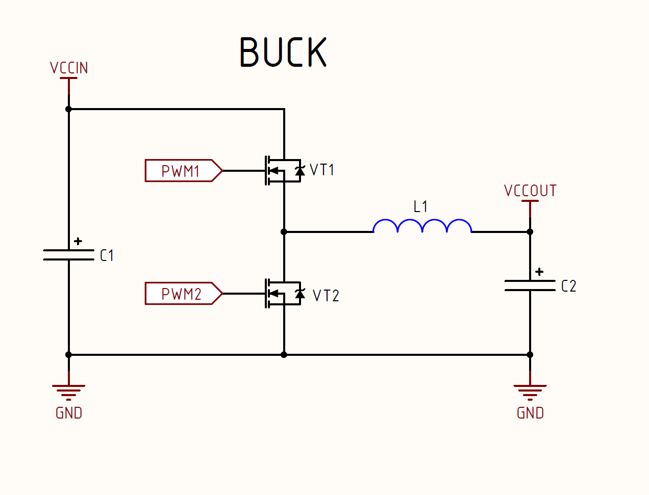
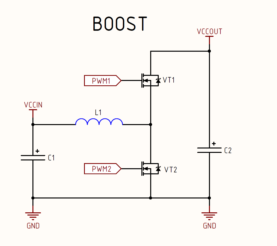
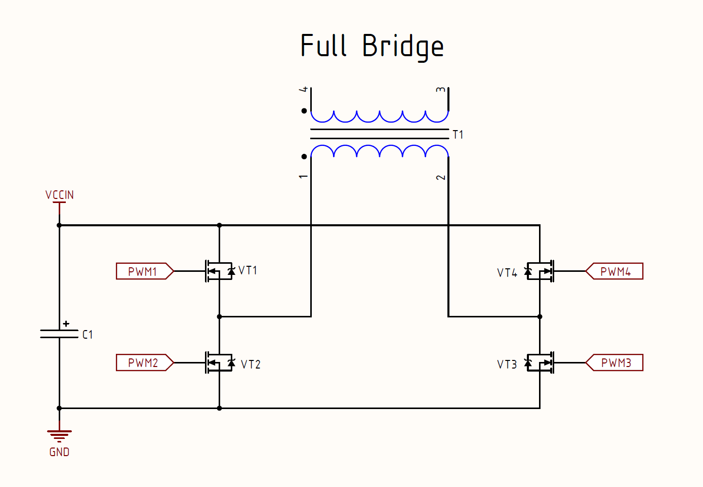
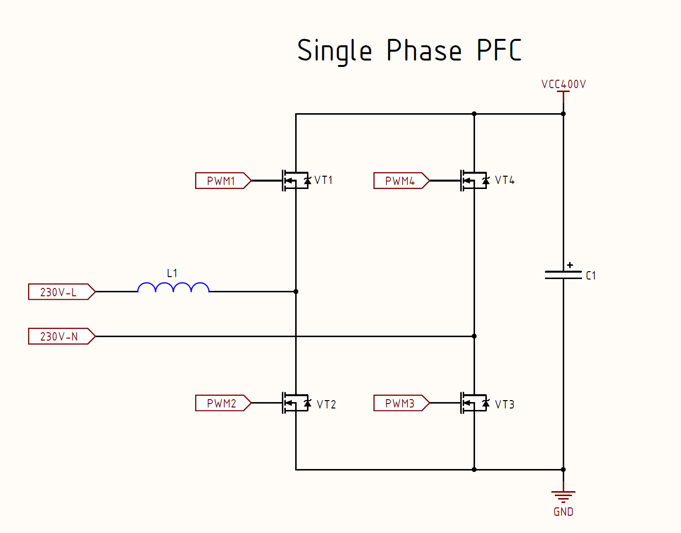

Now look carefully again. I drew specially without strapping, only the key components to make it clearer. What is common in these topologies? The first thing that strikes you is a series of general points:
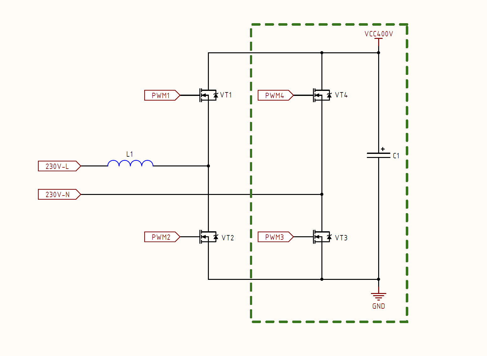
From this we can conclude that with a standard module in the form of a bundle “half-bridge + capacitor”, you can build any converter, adding only the desired choke or transformer. Therefore, the obvious solution to simplify prototyping was the creation of such a module:
Unfortunately, a limited number of hours per day and banal laziness dictate their conditions. I came to the need to make this module a year ago, but the implementation was constantly being transferred under the slogan - “I will definitely do it next weekend!” .
Perhaps the idea would have remained on the shelf if it were not for 2 events. First, 2 customers came to me in one month and everyone wanted a complex and interesting converter in its implementation, and most importantly they were ready to pay very well. Although considering that he is from Europe, it could have turned out to be even cheaper for them)) Both projects were interesting for me, for example, one of them was “three-phase voltage stabilizer with electrical isolation (sic!)”, That is, 3-phase PFC + 3 bridge converters (phase shifted) + synchronous rectifier + 3-phase inverter. All this on SiC and very compact. In general, I took 2 large orders, each of them for ~ 800 man-hours and a period of 6 months. As a result, I was “forced” to look for ways to optimize.
Secondly, guys from PCBway wrote to me unexpectedly ., many of them probably ordered the board, and offered to cooperate. They very actively support open-source hardware projects, that is, the very initiative of CERN - Open Source Hardware. Cooperation is simple, understandable for both parties - they supply me with free boards for my projects, and I open them, well, I post them on their website, in other places already at will. For me, this has become an additional motivation, and most importantly my conscience is clear, because I have been ordering boards and prototypes from them for several years, and for mass production I also tell them to my friends and partners. Now I’ve got a bun in the form of free boards for small projects for this, you can write to Habr more often))
And then the ice started, it was decided to create not just the module described earlier, but a whole set of the developer of power electronics and make it open and accessible to everyone.
At the beginning of the article, I mentioned that I will tell today only about one part - this is the power module of the half bridge . He alone allows you to create a converter, simply by screwing a control circuit, for example, debugging STM32-Discovery, Arduino, TMS320, TL494 or what you own there. Binding to any platform or MK is not at all.
Only this is not the whole project, but part)) What is the finished power converter made of? First of all, the power unit, in order for it to work, a certain control module is needed to understand what is happening, an indication is needed, and in order to understand what is happening from a safe distance, an interface, for example, Modbus RTU or CAN, is needed.
As a result, the overall structure of the project looks like this:
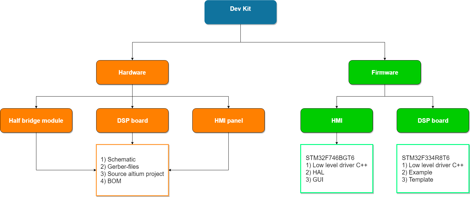
Probably in the future I will also write a program for calculating transformers and chokes, both conventional and planar. So far so. Different parts of the diagram in draft form have already been implemented and run-in in two projects, after minor improvements, articles will also be written on them and source codes will be available.
Now it's time to take a closer look at today's hero. The module is universal and allows working with Mosfet and IGBT transistors, with both low-voltage and high-voltage switches up to 1200V.
Module features:
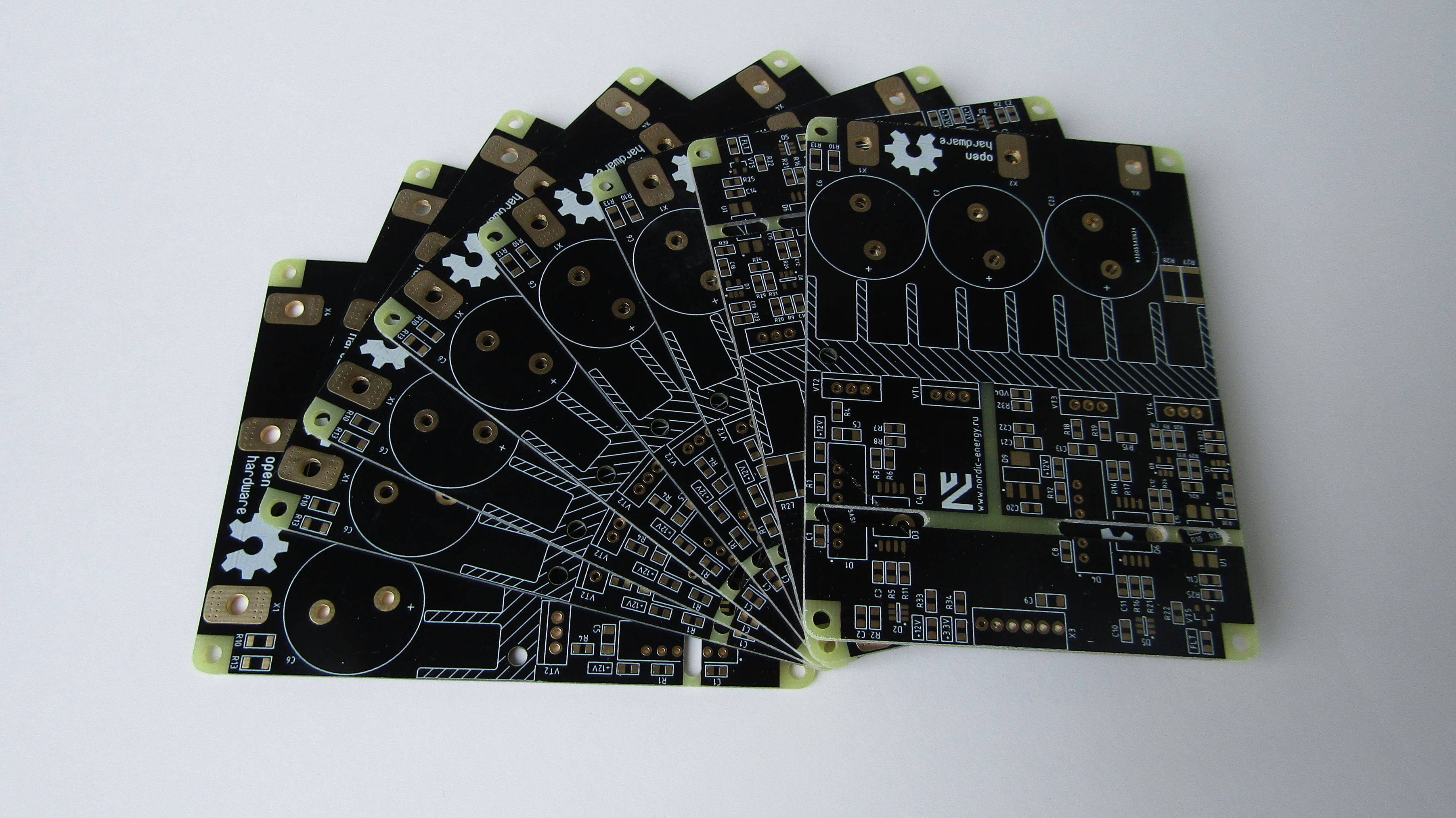
The article features the 1st revision of the module, it is fully working, but there will be a 2nd revision, in which purely constructive shortcomings are eliminated and the connectors are changed to more convenient ones. After completing the creation of the documentation, I threw the gerber into the PCBway and after 6 days the courier knocked on the door and handed me such delight: A week later, the accessories from one excellent domestic store were finally broughtto the dogs . As a result, everything was mounted:
Before moving on, let's look at the module schematic diagram. You can download it here - PDF .


There is nothing complicated or magical. Normal half bridge: 2 keys at the bottom, 2 at the top, you can solder one by one. The driver as above wrote from the family 1ED, very angry and immortal. Everywhere on the power there is an indication, including + 12V output dc / dc. The protection is implemented on the AND logical element, in case of overcurrent, the comparator will give out + 3.3V, they will light the optocoupler and it will pull one of the AND inputs to the ground, which means establishing log.0 and the PWM signal from the drivers will disappear. AND with 3 inputs is used specially, in the next revision I plan to make also protection against radiator overheating and get the error signal there too. All sources will be at the end of the article.
I thought for a long time on how to demonstrate the work of the module, so that it is not too boring, and useful, and not very difficult, so that anyone can repeat it. Therefore, I stopped at the voltage inverter, they are used to work with solar panels, if something bangs on the low-voltage side - not terrible, but on the high-voltage side - just when you turn it on, do not put your hands in it.
The inverter itself is outrageously simple, by the way, MAP Energia rivet just such, here's an example of even the commercial realization of this idea. The operation of the inverter is to form from a constant voltage of 12V alternating sinusoidal form with a frequency of 50 Hz, because the usual transformer at 50 Hz is used to work with just that. I use some kind of Soviet, like OSM, 220V factory winding and is used as a secondary, and the primary ~ 8V is wound with a copper bus. It looks like this:
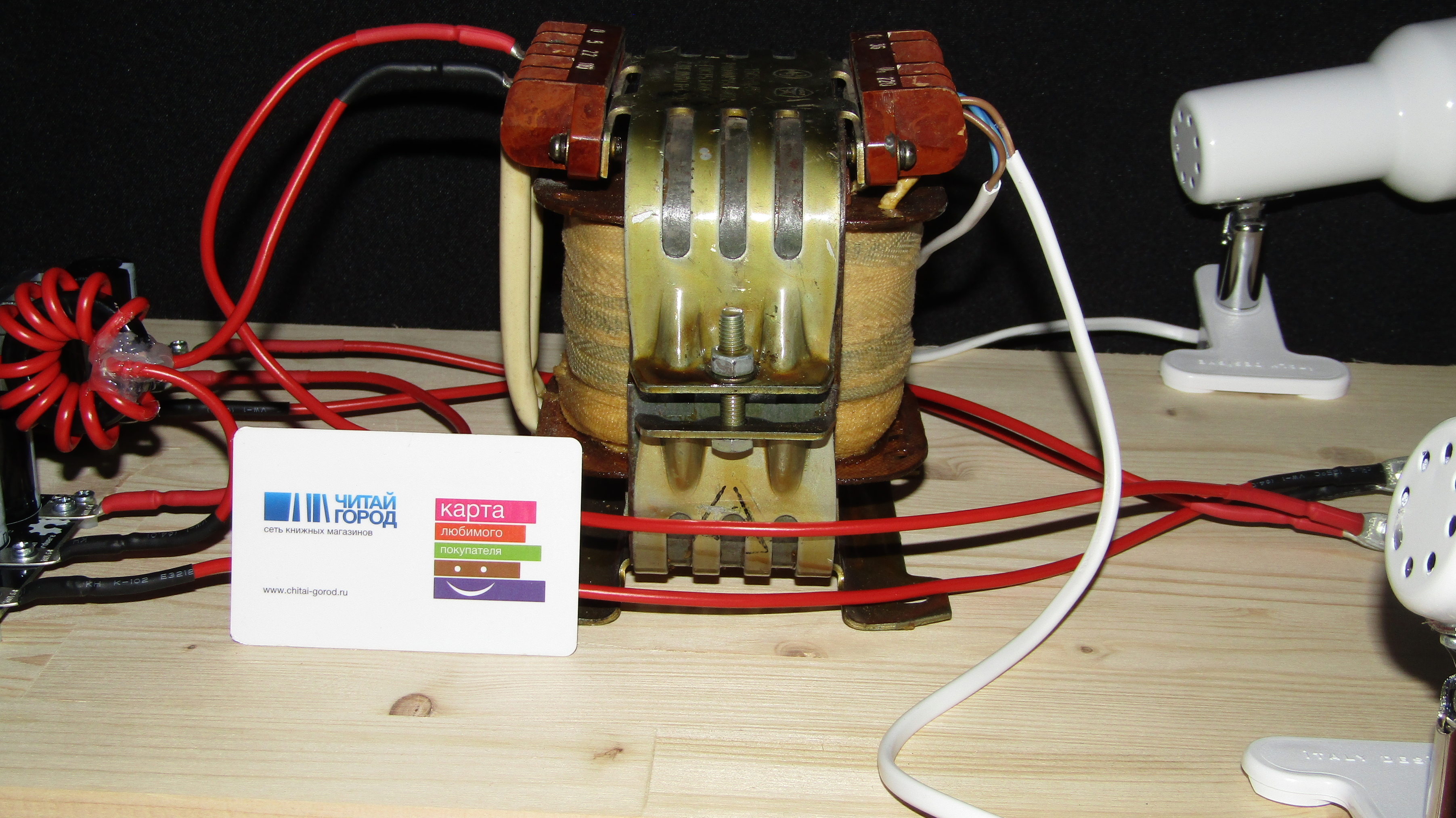
And this monster is only 400 watts! The weight of the transformer is about 5-7 kg. Actually, this is the minus of inverters with "iron" transformers, they are huge and heavy. Plus them is that these inverters are soooo simple, do not require any experience to create and of course are cheap.
Now let's connect the modules and the transformer. In fact, the module for the developer should be presented simply as a “black box” that has an input of 2 PWMs and 3 power outputs: VCC, GND and the actual output of the half bridge.

Now, from these “black boxes”, let's draw our inverter:

Yeah, it took only 3 external elements: a transformer + LC filter. For the latter, I manufactured a choke simply by winding a wire from the module to the transformer on a ring of Kool Mu material, size R32, with permeability 60, inductance about 10 μH. Of course, the throttle should be calculated, but we need 15 minutes later)) In general, if you drive something like 400 W, then you need a ring of R46 size (this is the outer diameter). Capacity - 1-10 microfarad film, that's enough. In fact, you can not put a capacitor as a saving, because the capacity of the transformer winding is healthy ... in general, the Chinese and MAP did just that)) The choke looks like this:

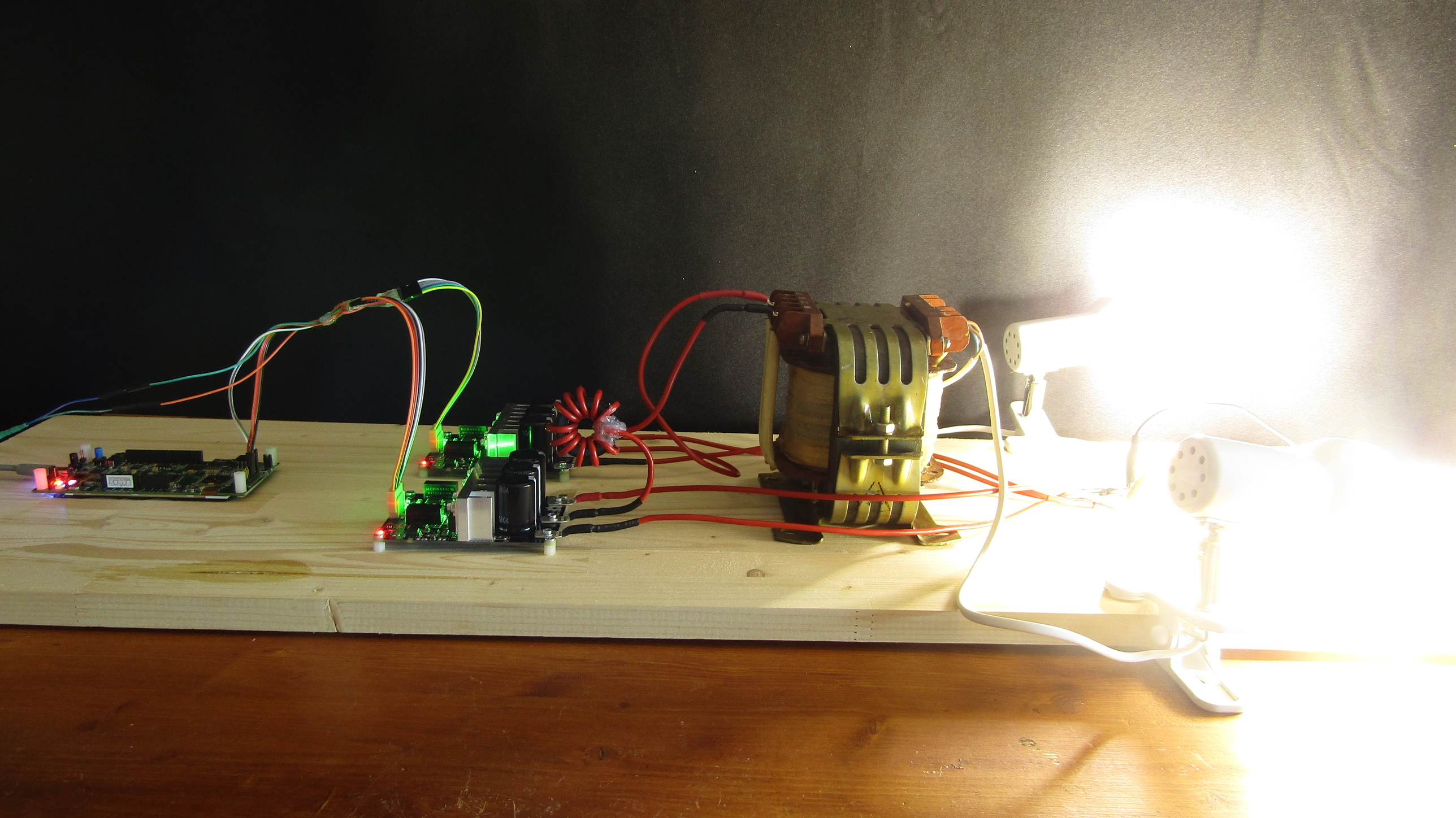
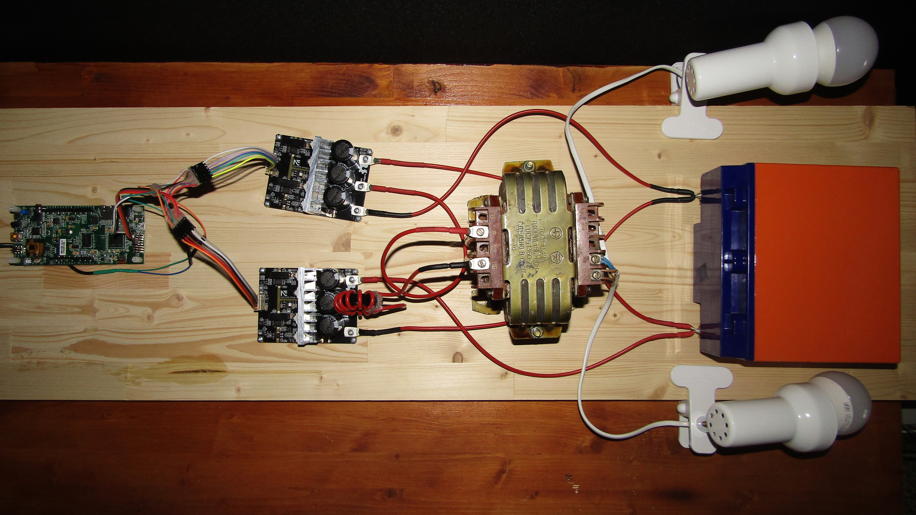
It remains to throw a test load on the output, I have a pair of 20 W LED bulbs (nothing visual was at hand), they themselves eat 24W, however, the efficiency. Also the no-load current of the transformer is about 1A. With the battery will eat about 5A. As a result, we have such a stand: The Delta HR12-17 battery is also used in the layout, respectively, at 12V and with a capacity of 17 Ah. We will control the converter from the STM32F469-Discovery debug board.
Initially, it was supposed to use my STM32VL-Disco for management, obtained at the exhibition back in 2010, but it so happened that it was on this layout that she was destined to die when all the code was written and the layout was launched. I forgot about oscilloscope probes and combined 2 lands, amen. In the end, everything was rewritten on the STM32F469NIH6, it was this debugging that was at hand, so there will be 2 projects: for the F100 and for the F469, both are checked. The project is compiled for TrueSTUDIO, version of the Eclipse from ST.
In general, in his other article he sooo described in detail and clearly how to form a sinusoidal signal, how to write code, and so on. You can read - here .
Read? Want to collect? Keep the project:
We launch the code, we arm ourselves with an oscilloscope and go further. First of all, we check for the presence of a signal at the driver input, it should be like this:
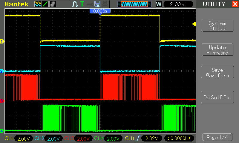
It should be noted that I am sending two signals to one half-bridge (module), drawing a sine, and to the other 2 signals defining 50 Hz. Moreover, one diagonal is “red + yellow” and the other is “blue + green”. The article that gave above about this is written in detail, if you suddenly do not understand. Now, as we have given signals, we throw on both half-bridges + 12V and GND from the laboratory power supply unit. Immediately I do not advise the battery, if something is mistaken, it can burn something. The protection on the board saves from overcurrent, but not from obvious jambs, when plus and minus are mixed up, but the lab is saving. 12V and 1A for tests is enough. We take the oscilloscope probe, its earth wire to the output of the first half-bridge, and the probe itself to the output of the other half-bridge should be such a picture:

Where is the sine you ask? The fact is that the resistance of the oscilloscope input is large and it does not constitute a load, so the current does not flow and the sine does not come from. Add the load, I made 10 ohm resistors with a 90 ohm load by simply connecting 9 pieces in series. We cling to the outputs of the half-bridges and see the following picture:

Do you have the same? So it's time to connect the choke, transformer, load and try to start. Achtung! You can not include this layout without load, because at idle at the exit can be up to 350 ... 380V. So that this does not need a load or OS. We will not have the last one, this is the topic of a separate article, you can fasten the simplest P-regulator as an elective, you already have a project template.
After switching on, we get about 230V at the output, the output is of course not stabilized, and it will float 230V + -30V, it will go for tests, in another article we will refine the layout and decide how to tell about P and PI controllers and their implementation.
Now you can enjoy the result of the work, and if necessary, pack everything in a box and even apply it on the farm or in the country to provide yourself with light and other delights.
You probably noticed a delay between the "click", that is, the power to the Discovery and the inclusion of lamps - this is the time that MK spent on initialization. This delay can be reduced by writing a single digit to the register at once, rather than splitting the register entry into a bunch of lines. I shattered solely for clarity. Although it is not scary, with the code on HAL the delay is 3 times longer and the people somehow live with it))
Until I forgot, the source code of the project:
It remains to see how there are temperatures on the board, whether there are any particularly hot places. 5-6A is of course not enough, but if the through current goes or some serious error, then that will be enough to turn the board into a kettle:
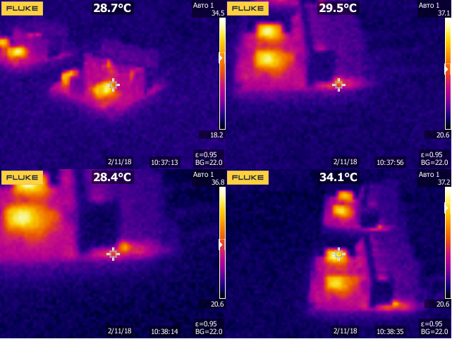
As you can see, the hottest element is the dc / dc module for electrical isolation, which is 2 W, it heats up right up to 34 degrees, well, even a shunt. The transistors themselves and the radiator have an ambient temperature after 30 minutes of the converter operation))
In the near future, I plan to write about the DSP board and to manage it no longer from debug discovery, but already from a “specialized” module. The 2nd revision boards have already come to it from the same PCBway, waiting for the components and writing right away.
I hope the article and the idea you liked. In the future, on the same modules, I will show how to assemble the frequency counter, the mppt controller, and maybe something else interesting. If you have questions, do not hesitate to ask them in the comments or in a personal, if you suddenly do not have a full account, I will try to answer all the questions.
Now a few thanks to the company PCBway , in fact, it’s very good that they support open source development. Zheleznyachniki may even catch up with the software on the quantity and quality of open source projects.

Development of power electronics for several reasons is one of the most difficult areas of electronics - the cost of error here is very high, while the development of power converters has always attracted amateurs, DIY engineers and not only. Surely you wanted to build a powerful power supply for some of your project? Or maybe online UPS for a couple of kW and not go broke? Or maybe chastotnik to the workshop?
Today I will talk about my small open project, or rather about its part, which will allow anyone who wants to step into the world of power electronics development and stay alive. As a demonstration of the possibilities, I will show you how to assemble a voltage inverter from 12V DC to 230V AC with a sine at the output in 15 minutes. Intrigued? Go!

The reasons for the appearance of the project
In the last couple of years, the development of power converters makes up about 90% of my orders, the main labor costs are mainly spent on software development and prototyping, circuit design + final trace of the board from the total costs is usually no more than 10-15%. Here comes the understanding that the prototyping process, which includes software development, needs to be somehow reduced and optimized.
As always, there are at least two ways out: to buy ready-made debugging, for example, from Texas Instrumets or Infineon, but they are usually sharpened for a specific task and cost from $ 500 to $ 5000, but there is no guarantee that there will be a similar order and this investment with high probability just will not pay off.
The second option is to do it yourself, but doing it thoroughly is almost the same thing as running “+1 revision of hardware”, which will result in additional expenses for the customer. If you do not do it thoroughly, then as usual everything will be on snot and somewhere something will fall off and while the layout, components and terms.
After some time, I noticed an obvious solution. It is so simple and obvious that for a long time I wondered why the same TI or Infineon had not done this yet. Now I will tell about my "enlightenment".
Let's look at some of the most popular topologies of power converters:


Now look carefully again. I drew specially without strapping, only the key components to make it clearer. What is common in these topologies? The first thing that strikes you is a series of general points:
- All topologies include the main components - capacitors, transistors and inductance (choke or transformer). These are 3 whales of power electronics;
- Transistors are switched on everywhere in the same way and form the so-called "half bridge". Almost all converter topologies are built from it;
- The option of switching on the “half-bridge + capacitor” bundle does not change on all topologies. The type of inductance and options for the inclusion of half-bridges is changing.
From this we can conclude that with a standard module in the form of a bundle “half-bridge + capacitor”, you can build any converter, adding only the desired choke or transformer. Therefore, the obvious solution to simplify prototyping was the creation of such a module:

The struggle between good and evil
Unfortunately, a limited number of hours per day and banal laziness dictate their conditions. I came to the need to make this module a year ago, but the implementation was constantly being transferred under the slogan - “I will definitely do it next weekend!” .
Perhaps the idea would have remained on the shelf if it were not for 2 events. First, 2 customers came to me in one month and everyone wanted a complex and interesting converter in its implementation, and most importantly they were ready to pay very well. Although considering that he is from Europe, it could have turned out to be even cheaper for them)) Both projects were interesting for me, for example, one of them was “three-phase voltage stabilizer with electrical isolation (sic!)”, That is, 3-phase PFC + 3 bridge converters (phase shifted) + synchronous rectifier + 3-phase inverter. All this on SiC and very compact. In general, I took 2 large orders, each of them for ~ 800 man-hours and a period of 6 months. As a result, I was “forced” to look for ways to optimize.
Secondly, guys from PCBway wrote to me unexpectedly ., many of them probably ordered the board, and offered to cooperate. They very actively support open-source hardware projects, that is, the very initiative of CERN - Open Source Hardware. Cooperation is simple, understandable for both parties - they supply me with free boards for my projects, and I open them, well, I post them on their website, in other places already at will. For me, this has become an additional motivation, and most importantly my conscience is clear, because I have been ordering boards and prototypes from them for several years, and for mass production I also tell them to my friends and partners. Now I’ve got a bun in the form of free boards for small projects for this, you can write to Habr more often))
And then the ice started, it was decided to create not just the module described earlier, but a whole set of the developer of power electronics and make it open and accessible to everyone.
Project structure
At the beginning of the article, I mentioned that I will tell today only about one part - this is the power module of the half bridge . He alone allows you to create a converter, simply by screwing a control circuit, for example, debugging STM32-Discovery, Arduino, TMS320, TL494 or what you own there. Binding to any platform or MK is not at all.
Only this is not the whole project, but part)) What is the finished power converter made of? First of all, the power unit, in order for it to work, a certain control module is needed to understand what is happening, an indication is needed, and in order to understand what is happening from a safe distance, an interface, for example, Modbus RTU or CAN, is needed.
As a result, the overall structure of the project looks like this:

Probably in the future I will also write a program for calculating transformers and chokes, both conventional and planar. So far so. Different parts of the diagram in draft form have already been implemented and run-in in two projects, after minor improvements, articles will also be written on them and source codes will be available.
Half bridge power module
Now it's time to take a closer look at today's hero. The module is universal and allows working with Mosfet and IGBT transistors, with both low-voltage and high-voltage switches up to 1200V.
Module features:
- Galvanic isolation of the control (digital) side from the power. Insulation breakdown voltage 3 kV;
- The upper and lower keys are independent, each has its own galvanically isolated driver and galvanically isolated dc / dc;
- A modern driver from Infineon is used - 1EDC60I12AHXUMA1. Pulse current opening / closing - 6A / 10A. The maximum frequency is 1 MHz (tested up to 1.5 MHz is stable);
- Current protection: shunt + op-amp + comparator + optocoupler;
- The maximum current is 20A. Limited not by keys, but by the size of the radiator and the thickness of the copper polygons.
The article features the 1st revision of the module, it is fully working, but there will be a 2nd revision, in which purely constructive shortcomings are eliminated and the connectors are changed to more convenient ones. After completing the creation of the documentation, I threw the gerber into the PCBway and after 6 days the courier knocked on the door and handed me such delight: A week later, the accessories from one excellent domestic store were finally brought


There is nothing complicated or magical. Normal half bridge: 2 keys at the bottom, 2 at the top, you can solder one by one. The driver as above wrote from the family 1ED, very angry and immortal. Everywhere on the power there is an indication, including + 12V output dc / dc. The protection is implemented on the AND logical element, in case of overcurrent, the comparator will give out + 3.3V, they will light the optocoupler and it will pull one of the AND inputs to the ground, which means establishing log.0 and the PWM signal from the drivers will disappear. AND with 3 inputs is used specially, in the next revision I plan to make also protection against radiator overheating and get the error signal there too. All sources will be at the end of the article.
We collect the model of the inverter
I thought for a long time on how to demonstrate the work of the module, so that it is not too boring, and useful, and not very difficult, so that anyone can repeat it. Therefore, I stopped at the voltage inverter, they are used to work with solar panels, if something bangs on the low-voltage side - not terrible, but on the high-voltage side - just when you turn it on, do not put your hands in it.
The inverter itself is outrageously simple, by the way, MAP Energia rivet just such, here's an example of even the commercial realization of this idea. The operation of the inverter is to form from a constant voltage of 12V alternating sinusoidal form with a frequency of 50 Hz, because the usual transformer at 50 Hz is used to work with just that. I use some kind of Soviet, like OSM, 220V factory winding and is used as a secondary, and the primary ~ 8V is wound with a copper bus. It looks like this:

And this monster is only 400 watts! The weight of the transformer is about 5-7 kg. Actually, this is the minus of inverters with "iron" transformers, they are huge and heavy. Plus them is that these inverters are soooo simple, do not require any experience to create and of course are cheap.
Now let's connect the modules and the transformer. In fact, the module for the developer should be presented simply as a “black box” that has an input of 2 PWMs and 3 power outputs: VCC, GND and the actual output of the half bridge.

Now, from these “black boxes”, let's draw our inverter:

Yeah, it took only 3 external elements: a transformer + LC filter. For the latter, I manufactured a choke simply by winding a wire from the module to the transformer on a ring of Kool Mu material, size R32, with permeability 60, inductance about 10 μH. Of course, the throttle should be calculated, but we need 15 minutes later)) In general, if you drive something like 400 W, then you need a ring of R46 size (this is the outer diameter). Capacity - 1-10 microfarad film, that's enough. In fact, you can not put a capacitor as a saving, because the capacity of the transformer winding is healthy ... in general, the Chinese and MAP did just that)) The choke looks like this:

It remains to throw a test load on the output, I have a pair of 20 W LED bulbs (nothing visual was at hand), they themselves eat 24W, however, the efficiency. Also the no-load current of the transformer is about 1A. With the battery will eat about 5A. As a result, we have such a stand: The Delta HR12-17 battery is also used in the layout, respectively, at 12V and with a capacity of 17 Ah. We will control the converter from the STM32F469-Discovery debug board.

Code
Initially, it was supposed to use my STM32VL-Disco for management, obtained at the exhibition back in 2010, but it so happened that it was on this layout that she was destined to die when all the code was written and the layout was launched. I forgot about oscilloscope probes and combined 2 lands, amen. In the end, everything was rewritten on the STM32F469NIH6, it was this debugging that was at hand, so there will be 2 projects: for the F100 and for the F469, both are checked. The project is compiled for TrueSTUDIO, version of the Eclipse from ST.
Footcloth code
#include"main.h"/********************************************* Sinus table **********************************************************/uint16_t sinData[240] =
{0,13,26,39,52,65,78,91,104,117,130,143,156,169,182,195,207,220,233,246,258,271,284,296,309,321,333,346,358,370,
382,394,406,418,430,442,453,465,477,488,500,511,522,533,544,555,566,577,587,598,608,619,629,639,649,659,669,678,688,697,
707,716,725,734,743,751,760,768,777,785,793,801,809,816,824,831,838,845,852,859,866,872,878,884,891,896,902,908,913,918,
923,928,933,938,942,946,951,955,958,962,965,969,972,975,978,980,983,985,987,989,991,993,994,995,996,997,998,999,999,999,
999,999,999,998,997,996,995,994,993,991,989,987,985,983,980,978,975,972,969,965,962,958,955,951,946,942,938,933,928,923,
918,913,908,902,896,891,884,878,872,866,859,852,845,838,831,824,816,809,801,793,785,777,768,760,751,743,734,725,716,707,
697,688,678,669,659,649,639,629,619,608,598,587,577,566,555,544,533,522,511,500,488,477,465,453,442,430,418,406,394,382,
370,358,346,333,321,309,296,284,271,258,246,233,220,207,195,182,169,156,143,130,117,104,91,78,65,52,39,26,13,0};
uint16_t sinStep;
uint8_t sinStatus;
/******************************************** Used functions ********************************************************/voidStartInitClock(void){
	RCC->CR |= RCC_CR_HSEON; 																				// Enable HSEwhile (!(RCC->CR & RCC_CR_HSERDY));
	FLASH->ACR |= FLASH_ACR_LATENCY_5WS;
	RCC->PLLCFGR = 0x00;
	RCC->PLLCFGR |= RCC_PLLCFGR_PLLM_3; 																	// Div for HSE = 8
	RCC->PLLCFGR |= RCC_PLLCFGR_PLLN_4 | RCC_PLLCFGR_PLLN_5 | RCC_PLLCFGR_PLLN_6 | RCC_PLLCFGR_PLLN_7;		// PLL mult x240
	RCC->PLLCFGR |= RCC_PLLCFGR_PLLSRC;																		// Source HSE
	RCC->CR |= RCC_CR_PLLON;
	while((RCC->CR & RCC_CR_PLLRDY) == 0){}
	RCC->CFGR &= ~RCC_CFGR_SW;
	RCC->CFGR |= RCC_CFGR_SW_PLL; 																			// Select source SYSCLK = PLLwhile((RCC->CFGR & RCC_CFGR_SWS) != RCC_CFGR_SWS_1) {} 													// Wait till PLL is used
	RCC->CR |= RCC_CR_PLLSAION;
	while ((RCC->CR & RCC_CR_PLLSAIRDY) == 0) {}
}
voidEnableOutputMCO(void){
	RCC->AHB1ENR |= RCC_AHB1ENR_GPIOAEN;						// Enable clock port A
	GPIOA->MODER   &= ~GPIO_MODER_MODER8;
	GPIOA->MODER   |= GPIO_MODER_MODER8_1;						// Alternative PP
	GPIOA->OSPEEDR |= GPIO_OSPEEDER_OSPEEDR8;					// Very high speed
	RCC->CFGR |= RCC_CFGR_MCO1;									// Source PLL
	RCC->CFGR &= ~RCC_CFGR_MCO1PRE;								// Div = 1
}
voidInitIndicatorLED(void){
	/*
	 * LED1 - PG6
	 * LED2 - PD4
	 * LED3 - PD5
	 * LED4 - PK3
	 */
	RCC->AHB1ENR |= RCC_AHB1ENR_GPIOGEN;
	RCC->AHB1ENR |= RCC_AHB1ENR_GPIODEN;
	RCC->AHB1ENR |= RCC_AHB1ENR_GPIOKEN;
	GPIOG->MODER &= ~GPIO_MODER_MODER6;
	GPIOG->MODER |= GPIO_MODER_MODER6_0;		// Output PP
	GPIOD->MODER &= ~GPIO_MODER_MODER4;
	GPIOD->MODER |= GPIO_MODER_MODER4_0;		// Output PP
	GPIOD->MODER &= ~GPIO_MODER_MODER5;
	GPIOD->MODER |= GPIO_MODER_MODER5_0;		// Output PP
	GPIOK->MODER &= ~GPIO_MODER_MODER3;
	GPIOK->MODER |= GPIO_MODER_MODER3_0;		// Output PP
}
voidEnableIndicatorLED(void){
	GPIOG->BSRR |= GPIO_BSRR_BR_6;
	GPIOD->BSRR |= GPIO_BSRR_BR_4;
	GPIOD->BSRR |= GPIO_BSRR_BR_5;
	GPIOK->BSRR |= GPIO_BSRR_BR_3;
}
voidInitLowPWM(void){
	/*
	 * TIM1-CH1  - PA8
	 * TIM1-CH1N - PB13
	 */
	RCC->APB2ENR |= RCC_APB2ENR_TIM1EN;
	RCC->AHB1ENR |= RCC_AHB1ENR_GPIOAEN;
	RCC->AHB1ENR |= RCC_AHB1ENR_GPIOBEN;
	/*********** GPIO **********/
	GPIOA->MODER &= ~GPIO_MODER_MODER8;
	GPIOA->MODER |= GPIO_MODER_MODER8_1;												// Alternative output PP
	GPIOA->AFR[1] |= GPIO_AFRH_AFRH0_0;													// Select TIM1-CH1
	GPIOB->MODER &= ~GPIO_MODER_MODER13;
	GPIOB->MODER |= GPIO_MODER_MODER13_1;												// Alternative output PP
	GPIOB->AFR[1] |= GPIO_AFRH_AFRH5_0;													// Select TIM1-CH1N/*********** Timer *********/
	TIM1->PSC = 2400-1;																	// div for clock: F = SYSCLK / [PSC + 1]
	TIM1->ARR = 1000;																	// count to 1000
	TIM1->CR1 &= ~TIM_CR1_CKD;															// div for dead-time: Tdts = 1/Fosc = 41.6 ns
	TIM1->CCR1 = 500;																	// duty cycle 50%
	TIM1->CCER |= TIM_CCER_CC1E | TIM_CCER_CC1NE;   									// enable PWM complementary out to PB15 and to PA10
	TIM1->CCER &= ~TIM_CCER_CC1NP; 														// active high level: 0 - high, 1 - low
	TIM1->CCMR1 &= ~TIM_CCMR1_OC1M;
	TIM1->CCMR1 |= TIM_CCMR1_OC1M_2 | TIM_CCMR1_OC1M_1;									// positiv PWM1_CH3 and PWM1_CH3N
	TIM1->BDTR &= ~TIM_BDTR_DTG;														// clear register
	TIM1->BDTR |= TIM_BDTR_DTG_2 | TIM_BDTR_DTG_1 | TIM_BDTR_DTG_0;						// value dead-time: = 31*Tdts = 32*41,6ns = 1.29us
	TIM1->BDTR |= TIM_BDTR_MOE | TIM_BDTR_AOE;											// enable generation output and dead-time
	TIM1->CR1 &= ~TIM_CR1_DIR;															// count up: 0 - up, 1 - down
	TIM1->CR1 &= ~TIM_CR1_CMS;															// aligned on the front signal: 00 - front; 01, 10, 11 - center
	TIM1->CR1 |= TIM_CR1_CEN;															// start count
}
voidInitSinusPWM(void){
	/*
	 * TIM3-CH1 - PB4
	 * TIM3-CH2 - PC7
	 */
	RCC->APB1ENR |= RCC_APB1ENR_TIM3EN;
	RCC->AHB1ENR |= RCC_AHB1ENR_GPIOBEN;
	RCC->AHB1ENR |= RCC_AHB1ENR_GPIOCEN;
	/*********** GPIO **********/
	GPIOB->MODER &= ~GPIO_MODER_MODER4;
	GPIOB->MODER |= GPIO_MODER_MODER4_1;												// Alternative output PP
	GPIOB->AFR[0] |= GPIO_AFRL_AFRL4_1;													// Select TIM3-CH1
	GPIOC->MODER &= ~GPIO_MODER_MODER7;
	GPIOC->MODER |= GPIO_MODER_MODER7_1;												// Alternative output PP
	GPIOC->AFR[0] |= GPIO_AFRL_AFRL7_1;													// Select TIM3-CH2/*********** Timer *********/
	TIM3->PSC = 5-1;																					// div for clock: F = SYSCLK / [PSC + 1]
	TIM3->ARR = 1000;																					// count to 1000
	TIM3->CCR1 = 0;																						// duty cycle 0%
	TIM3->CCR2 = 0;																						// duty cycle 0%
	TIM3->CCER |= TIM_CCER_CC1E;   																		// enable PWM out to PA8
	TIM3->CCER &= ~TIM_CCER_CC1P; 																		// active high level: 0 - high, 1 - low
	TIM3->CCER |= TIM_CCER_CC2E;   																		// enable PWM complementary out to PA9
	TIM3->CCER &= ~TIM_CCER_CC1P; 																		// active high level: 0 - high, 1 - low
	TIM3->CCMR1 &= ~(TIM_CCMR1_OC1M | TIM_CCMR1_OC2M);
	TIM3->CCMR1 |= TIM_CCMR1_OC1M_2 | TIM_CCMR1_OC1M_1 | TIM_CCMR1_OC2M_2 | TIM_CCMR1_OC2M_1;			// positiv PWM1_CH1 and PWM1_CH2
	TIM3->CR1 &= ~TIM_CR1_DIR;																			// count up: 0 - up, 1 - down
	TIM3->CR1 &= ~TIM_CR1_CMS;																			// aligned on the front signal: 00 - front; 01, 10, 11 - center
	TIM3->CR1 |= TIM_CR1_CEN;																			// start count
}
voidInitStepSinus(void){
	RCC->APB1ENR |= RCC_APB1ENR_TIM6EN;																	// enable clock for basic TIM6
	TIM6->PSC = 5-1;																					// div, frequency 24 kHz
	TIM6->ARR = 1000; 																					// count to 1000
	TIM6->DIER |= TIM_DIER_UIE; 																		// enable interrupt for timer
	TIM6->CR1 |= TIM_CR1_CEN; 																			// start count
	NVIC_EnableIRQ(TIM6_DAC_IRQn); 																		// enable interrupt TIM6_DAC_IRQn
}
/************************************* Main code *********************************************/intmain(void){
	StartInitClock();
//	EnableOutputMCO();
	InitIndicatorLED();
	InitLowPWM();
	InitSinusPWM();
	InitStepSinus();
	EnableIndicatorLED();
	while(1)
	{
	}
}
/****************************** Interrupts ******************************************************/voidTIM6_DAC_IRQHandler(void){
	TIM6->SR &= ~TIM_SR_UIF;
	if (sinStatus == 0) {TIM3->CCR1 = sinData[sinStep];}
	if (sinStatus == 1) {TIM3->CCR2 = sinData[sinStep];}
	sinStep++;
	if (sinStep >= 240) {
			sinStep = 0;
			sinStatus = sinStatus ? 0 : 1;
	}
}
In general, in his other article he sooo described in detail and clearly how to form a sinusoidal signal, how to write code, and so on. You can read - here .
Read? Want to collect? Keep the project:
We launch the code, we arm ourselves with an oscilloscope and go further. First of all, we check for the presence of a signal at the driver input, it should be like this:

It should be noted that I am sending two signals to one half-bridge (module), drawing a sine, and to the other 2 signals defining 50 Hz. Moreover, one diagonal is “red + yellow” and the other is “blue + green”. The article that gave above about this is written in detail, if you suddenly do not understand. Now, as we have given signals, we throw on both half-bridges + 12V and GND from the laboratory power supply unit. Immediately I do not advise the battery, if something is mistaken, it can burn something. The protection on the board saves from overcurrent, but not from obvious jambs, when plus and minus are mixed up, but the lab is saving. 12V and 1A for tests is enough. We take the oscilloscope probe, its earth wire to the output of the first half-bridge, and the probe itself to the output of the other half-bridge should be such a picture:

Where is the sine you ask? The fact is that the resistance of the oscilloscope input is large and it does not constitute a load, so the current does not flow and the sine does not come from. Add the load, I made 10 ohm resistors with a 90 ohm load by simply connecting 9 pieces in series. We cling to the outputs of the half-bridges and see the following picture:

Do you have the same? So it's time to connect the choke, transformer, load and try to start. Achtung! You can not include this layout without load, because at idle at the exit can be up to 350 ... 380V. So that this does not need a load or OS. We will not have the last one, this is the topic of a separate article, you can fasten the simplest P-regulator as an elective, you already have a project template.
Turning on
After switching on, we get about 230V at the output, the output is of course not stabilized, and it will float 230V + -30V, it will go for tests, in another article we will refine the layout and decide how to tell about P and PI controllers and their implementation.
Now you can enjoy the result of the work, and if necessary, pack everything in a box and even apply it on the farm or in the country to provide yourself with light and other delights.
You probably noticed a delay between the "click", that is, the power to the Discovery and the inclusion of lamps - this is the time that MK spent on initialization. This delay can be reduced by writing a single digit to the register at once, rather than splitting the register entry into a bunch of lines. I shattered solely for clarity. Although it is not scary, with the code on HAL the delay is 3 times longer and the people somehow live with it))
Until I forgot, the source code of the project:
It remains to see how there are temperatures on the board, whether there are any particularly hot places. 5-6A is of course not enough, but if the through current goes or some serious error, then that will be enough to turn the board into a kettle:

As you can see, the hottest element is the dc / dc module for electrical isolation, which is 2 W, it heats up right up to 34 degrees, well, even a shunt. The transistors themselves and the radiator have an ambient temperature after 30 minutes of the converter operation))
Thanks and plans
In the near future, I plan to write about the DSP board and to manage it no longer from debug discovery, but already from a “specialized” module. The 2nd revision boards have already come to it from the same PCBway, waiting for the components and writing right away.
I hope the article and the idea you liked. In the future, on the same modules, I will show how to assemble the frequency counter, the mppt controller, and maybe something else interesting. If you have questions, do not hesitate to ask them in the comments or in a personal, if you suddenly do not have a full account, I will try to answer all the questions.
Now a few thanks to the company PCBway , in fact, it’s very good that they support open source development. Zheleznyachniki may even catch up with the software on the quantity and quality of open source projects.

