
Spain Creates Non-Volatile Reprogrammable Photonic Chip for 6G and Quantum Technologies
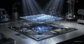
A research team from the Polytechnic University of Valencia, led by Professor José Capmany, has developed a photonic chip capable of operating at high speeds without the need for a constant power supply. The results, published in Nature Photonics, open up new possibilities for creating programmable integrated circuits in 6G telecommunications and quantum computing.
Insight Beyond the Hype: Analysis of the Spanish Non-Volatile Photonic Chip from José Capmany's Team
While the world was glued to WWDC and visits by big AI company CEOs to Korea, something different happened in Valencia. Quieter, more modest — and perhaps more important. A team led by Professor José Capmany from the Polytechnic University of Valencia published a result in Nature Photonics that, in two or three years, many will call a "turning point." And you know what? They'll be right.
The average person reads: "non-volatile reprogrammable chip." The insider sees: a death sentence for thermo-optic heaters and the dawn of an era where light learns to "remember" as well as silicon, but without overheating. This is not just another chip. This is a break from the canon that has governed photonic integrated circuitry for the last 15 years.
The Essence: What's Really Happening
Capmany and his team solved a fundamental problem that has been stifling the scaling of photonic processors. Until today, any programmable photonic chip (essentially a "microprocessor for light") required constant heating of microscopic resistors to change the phase of light — the so-called thermo-optic effect. Each such heater consumes energy, heats the package, and makes it impossible to create chips with thousands of components.
The researchers replaced the architecture. Instead of constant heating, they used a hybrid platform of silicon + barium titanate (BaTiO₃). This is a ferroelectric material: it retains polarization (and thus the configured optical state) after power is removed. Roughly speaking, they created an analog of non-volatile flash memory for light, but at the level of switching optical paths.
The numbers are telling. Switching time is on the order of 80 nanoseconds. That's two orders of magnitude better than any thermo-optic system (which operates in microseconds). Static power consumption is virtually zero. In current technologies, each element of a programmable matrix requires watts of heat 24/7. Here, the configuration requires no power at all.
Timeline and Context
Capmany's team is not new to the game. They have long been world leaders in programmable photonics. The spin-off company iPronics, co-founded by Capmany, closed a €20 million round in 2025 with participation from Triatomic Capital and has already been testing its solutions with Vodafone.
However, the current publication in Nature Photonics is the result of a consortium:
| Participant | Role | Country |
|---|---|---|
| Lumiphase AG | Materials supplier | Switzerland |
| CEA Leti | Silicon photonics prototype manufacturing | France |
| Greek university | Scientific partner | Greece |
This is Europe's answer to the US and China's monopoly in chip manufacturing.
Important context: April 2026. Just two months ago, the same Capmany team published a new information theory in Advanced Photonics — "Analog Photonic Information" (API) — and introduced the concept of "anbit" (analog bit). This anbit can carry 10–100 times more information than a digital bit, but requires fundamentally new hardware for processing. The chip announced now is the first physical embodiment of that theory. First the math (April 2026), now a working prototype (June 2026). A furious pace. Why is this important right now? Because the avalanche of data from AI, 6G, and the Internet of Things is simply overwhelming electronics. According to Capmany's own estimate, electronics have reached 85–90% of their physical limit. The race for the next decade is a race for photonics. The Spanish have just set a barrier.
Who Wins and Who Loses
Europe as a whole wins, and Spain in particular. Europe already has three megaprojects for photonic chip factories: Vigo (III-V materials), Barcelona (silicon), and Valencia (hybrid silicon-barium titanate). Now Valencia has not just a factory, but an architectural advantage. CEA Leti (France) participated in the development — so France will get this know-how for its lines.
iPronics wins. The commercial arm of the lab. Their CTO Daniel Pérez directly states "overcoming the main obstacle." With such a chip, iPronics can sell not just a "photonic FPGA," but a "photonic FPGA that doesn't heat up and doesn't consume electricity when idle." For data centers, where electricity bills are the second largest expense after salaries, this is an offer they can't refuse.
Developers of 6G and quantum technologies win. 80 nanoseconds is fast enough for packet switching in data centers during failover. And the absence of heat is critical for quantum computing: any photonic integrated circuits for qubits suffer from parasitic heat. Now this barrier is removed.
Manufacturers of traditional thermo-optic chips lose. Startups and R&D centers that have invested billions in technologies based on doped silicon with heating. Their patents on "phase control via heat" become yesterday's news. Some (like Klein Tools or LioniX) will have to urgently switch to barium titanate.
NVIDIA loses (partially). It sounds crazy, but the trend is clear. Photonic accelerators for AI are gradually becoming a reality. While NVIDIA dominates, photonics enables analog computing at tremendous speed. If iPronics scales its chip to thousands of programmable elements, some linear algebra tasks (matrix multiplication) will move from GPUs to photonic boards. A long-term threat, but it's taking shape right now.
What the Media Isn't Saying
And here's the main insight that no one writing about the "breakthrough in Spain" will see.
The media doesn't mention that barium titanate (BaTiO₃) is a notoriously finicky material in manufacturing. Its integration with silicon was considered "unsolvable" for mass production. Capmany's team, together with Lumiphase AG and CEA Leti, did what Intel and GlobalFoundries couldn't on their experimental lines. They found a way to deposit or grow BaTiO₃ on a standard silicon chip while preserving ferroelectric properties. If this process is transferred to commercial lines, it will open the door to a hybrid electronic-photonic architecture, where electronics control silicon and light processes data — with switching without heating.
Second nuance: 80 nanoseconds is good, but for CPUs it's still slow. A switching frequency of 12.5 MHz (1/80 ns) looks modest compared to gigahertz electronic transistors. This means: the chip won't replace logic, but will work as a reconfigurable optical matrix (flow router), not as a real-time computing core. But for 6G switching and reconfiguration of photonic processors, it's ideal.
Third nuance: static power consumption is zeroed, but dynamic (switching) still requires energy. Switching an 80-nanosecond gate still costs power. But the main achievement is elsewhere: previously, a chip with 1000 heaters consumed 100 W constantly. Now a chip with 1000 switches consumes 0 W in standby and only spikes during reconfiguration. For battery-powered IoT devices and portable quantum sensors, this is a game changer. Admit it, the difference is significant.
Forecast: Next 30 Days and 90 Days
30 days:
- Roadmap from iPronics. The company will announce plans for a commercial Field-Programmable Photonic Gate Array (FPPGA) on the new technology. Timeline: 18–24 months. Investment in the production line: around €30–40 million.
- Interest from hyperscalers. Google, AWS, and Microsoft (which have already tested iPronics prototypes) will request engineering samples for their data centers. Focus: using the chip for optical switching in large-scale AI clusters, where replacing electronic switches with photonic ones could save hundreds of megawatts.
- Scientific debate. Preprints from MIT and Caltech will emerge, criticizing the "long switching time" (80 ns vs. the "theoretical limit" of picoseconds from competitors using liquid crystals). A "photonic war" of publications will begin.
90 days (September 2026):
- Consolidation in the European photonic ecosystem. Given that the NEoteRIC project (biomedical photonics applications) is already using these chips, we will see the first commercial product: a portable spectrometer or blood analysis sensor powered by a non-volatile photonic chip. This will attract attention from pharmaceutical giants (Roche, Bayer).
- Start of negotiations with ASML. ASML (Netherlands) is interested in any optics for its EUV scanners. The BaTiO₃ technology from UPV could be used to create more precise and energy-efficient control elements in lithography machines.
- Patent pool. iPronics and UPV will file international patents for the "non-volatile field-programmable photonic gate array" architecture. This will create a protective barrier against Chinese competitors, who are still trying to solve the same problem with phase-change materials (GST, SbTe).
Conclusion for Strategists
What did José Capmany do? This is not just an engineering achievement. It's a translation of photonics from the category of "interesting lab technology" to "viable industrial alternative." Previously, programmable photonics hit a thermal barrier: to make a complex chip, you had to supply huge electrical power and solve heat dissipation. Now the barrier is gone. The chip can be scaled to thousands and tens of thousands of elements, creating true photonic processors that consume energy only when changing their configuration.
For Europe, which missed the electronic chip revolution (ASML being the only silver lining), this is a chance to carve out a niche in the next technological paradigm. For investors, it's a signal to look at companies working with BaTiO₃ and integrating ferroelectrics into standard CMOS lithography. Those who enter now will reap the rewards in three years, when 6G and post-silicon computing become mainstream.
— Editorial Team









No comments yet.