How we participated in InnovateFPGA 2018 and did not win again
Greetings, Habr! My name is Daniel Smirnov, I study at the graduate school of ITMO University, where in the programming and modeling laboratory our team is engaged in programmable electronics for projects related to fiber-optic sensors. FPGA - Field Programmable Gate Array is used as a hardware base for sensors. A couple of years ago, we learned that FPGA manufacturers are holding contests for engineering students. Since then, every year a team is formed from us to participate in this event, and since this year it turned out to be special, we decided to share how everything was from the inside.

It was October 2017, I did a weekly routine check: an analysis of ongoing conferences on topics that are implemented in our department. At one point, I receive a mailing list from Terasic: a new competition for developing projects using debug boards on FPGA , now worldwide, starts . The experience of the same contest of last year rushes and comes to mind: postponing the month to the last two weeks, long debugging and tuning of the algorithms and issuing all channels to the monitor and promising not to postpone it anymore to the last day.
It was a great experience, during which we learned a lot about such a platform as SoC FPGA - the union between a huge array of logic elements and the Cortex-A9 processor, as well as their interaction with each other and with the periphery on the debug board.
New competition - new rules, new requirements, new level. Now the competition is held in several stages: first, the regional stages are held, and then the final in San Jose; All participants are sent the same fee, the DE10-Nano , and in addition you can now choose not only the basic three modules, but also a large version of the Analog Devices boards! However, unlike contests in previous years, this time it is necessary to sign a guarantee for the project, and in case of non-fulfillment, participants must send the fees back. Quite rightly, given the statistics of past years:
To ensure that the project did not stand aside, it was decided to implement a device useful for the department, which then can be easily refined and improved. Based on the department's areas of activity, there were various options: optical reflectometer, stroboscopic oscilloscope, etc. Quickly reviewing already existing applications and available additional fees, it was revealed that the reflectometer was already stated, and a stroboscopic oscilloscope was not assembled on such elements. The only idea remained tenacious - vector network analyzer. The other day, a pair of coils was brought to the laboratory, for which there was no documentation. The task was to determine at least the approximate characteristics of these coils. It was known that they assembled an oscillatory circuit, so the main task was to find out the resonant frequency. In such tasks, a vector network analyzer (VAC or VNA - Vector Network Analyzer) can be used. VNA allows you to define a scattering matrix, also known as an S-parameter matrix. In this method, the element under study is considered as a black box, which analyzes the incident and reflected signals from the ports of this device. So, for a dual-port system, the matrix is as follows:
Where V1 + V2 + - electromagnetic waves arriving at the ports;
V1- V2– are electromagnetic waves emerging from the ports;
Sij - elements of the multipole scattering matrix. [2]
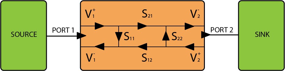
Scheme for measuring S-parameters of a multipole
The components and circuit could not be examined with X-rays (at least with metro X-rays), so the following scheme was assembled on the knees: frequencies were circulated to the coil input using a generator, the second port of the circulator was connected to the coil input, and the third input on the oscilloscope, which has in its software mode amplitude-frequency analysis. Such a scheme allows to measure the parameter S11, i.e. reflection. In the end, after long suffering and calibrations, it was possible to remove this characteristic - but at what price? The department had long anticipated the acquisition of a vector network analyzer for such tasks (measurements of the AFC of electronic devices), but this purchase was always somehow postponed.
After messing around with the coils, it was decided to assemble our own network analyzer with visualization and comfortable tuning. It’s easy to find the excitement and desire to learn something new for students and postgraduates working at the department, so the team was quickly assembled from an electronics engineer, a programmer on the chip, me and two mentors.
No sooner said than done! After numerous discussions about the frequency band, processing algorithms and other parameters of the project, the application contained the following:
To pass to the next stage, it was necessary for the project page to garner a sufficient number of “likes” from users registered on the site. At first, everything went well, but then some dubious projects began to gain unrealistic and contrasting values of likes and views compared to other projects. It turned out that the competition site was too vulnerable to cheating.
After some time, the organizers announced that the board of judges would still choose the finalists, so the likes of the users, in fact, lost their weight. On January 31, our team appeared in the lists of those passing to the next stage, and we began to think over our project in more detail in anticipation of debugging.
First came the DE10-Nano board. Nice, but a bit strange: expect that the boards will come all together. A few days later, a call comes in from customs: the fees came, they all together exceed the threshold for the price, so you need to pay an amount approximately equal to the cost of these fees for customs clearance. Such a deal disappointed us, but did not suit us: we refused the boards. In the presence of mixers and generators, we did not have, it is necessary to find new solutions. What to do? The first thing that came to my head was not the most accurate, but rather unusual solution: use the regular GPIO leg and generate a square wave from it. At the output of this leg, an analog low-pass filter is installed with a cut-off band slightly larger than the maximum frequency of the square wave. To start the analysis, it was suggested to start with 1 MHz (for example): then after the filter we would get a more or less pure sine (the higher harmonics would be cut off by the filter), and so on until the frequency drops to the one where there will be two harmonics in the signal after the filter. The meander is the sum of odd harmonics, and the proportional contribution of each harmonic is known in advance [3].
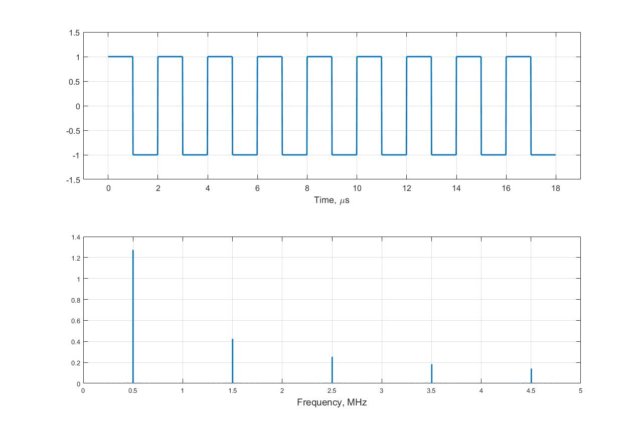
An example of the meander in the time and frequency domains: the spectrum shows the components of the harmonic signal at 500 kHz, 1.5 MHz, etc.
With a filter with a cut-off frequency of 1 MHz, you can go down to 33. (3) kHz. After this frequency for the filter, we should get the sum of two sines. The proportional ratio of their amplitudes is known (sinc-function), the response of the measured device to a frequency of 1 MHz (the first odd harmonic) also means that it remains for us to make an equation with one unknown and calculate the response characteristic at a frequency of 33, (3) kHz! At first, this solution seemed too simple, so for the beginning it was told to everyone in the hope that someone would find a mistake. No errors were found, but as the discussion proceeded, a number of restrictions were discovered:
Suppose we have solved all the problems on the analog part; programmatically, there are two others:
And finally, last but not least. The described scheme can be used if the measured element can be described by a linear transfer function. However, if we measure the black box with non-linear characteristics, there are more problems than ideas from the idea. There was not much time left (the first result should be shown two months after the arrival of the board), so after a brief reflection we decided to double-check our reserves on the debug boards already available - and found a 14-bit DAC at 125 Msps ! Not the most elegant solution, but you don’t have to choose, we use it as an output signal generator.
The selected DAC as a generator accepts data at the input of the parallel bus and latches it with a clock signal coming from the FPGA. Such a scheme is ideal for synchronization in our scheme. However, with the detection remained questions.
Yes, there is a 14-bit 65 Msps ADC on the same board. But here the potential of the generator is potentially higher, and according to Kotelnikov's theorem, this ADC will no longer work at maximum frequencies.
The solution was found during the discussion of this problem with experienced electronics engineers. It turned out that for our task we can use a synchronous detector circuit (lock-in amplifier): the output of such a detector are two constant values, the phase and quadrature components, from which the amplitude and phase of the signal can be obtained, and since they are constant, they can be detected even with the slow ADC installed on the DE10-Nano! It was decided to first model the circuit in LTSpice, and then select the components and assemble the circuit, taking into account that the detector input is a signal from the circulator, and the outputs are connected to the ADC on the DE10-Nano board.
Updated design concept
Sinusoidal signals with a frequency of 1 Hz to 1 MHz with steps of a few Hz sent to the first port of the circulator. The device under study was connected to the second port, depending on the frequency response of which the signal reflectance changed. The reflected signal arrived at port 3, where a synchronous detector circuit was assembled to determine the frequency and phase characteristics. For correct operation, the ports of the circulator were adapted for a 100 Ohm impedance, which was associated with the output resistance of the D / A converter and the choice of the devices under study.
Less than a month remained before the project was completed, and by the end of the term it was necessary to also prepare reporting materials: a detailed description of the project on the contest page, a project posted on GitHub in the public domain and a video report on the work done.
Since we now understood what data would be fed into the inputs and outputs, we began work on a project for SoC FPGA. We saw the project being implemented as follows: the user sets the frequency range in which the measurement is planned, the FPGA begins to generate harmonics in the specified interval in turn using a DAC, the ADC accepts quadrature and phase components at the input, converting them into the amplitude and phase values at the current frequency , the values obtained are displayed in real time on a monitor connected to the debug board. There had already been some groundwork on displaying information on the monitor, so the main part was to correctly draw the data in real time and display the picture on HDMI. We ungrouped. The first group took up tasks for the program for the processor, deal more with the necessary initializations, data visualization issues. We also asked them to raise the screen resolution to 1024x768 [6]. The second group contains details on the implementation of the part on the FPGA, which should then be brought to the processor via the lightweight_h2f interface bus, as well as testing the performance of the first prototype of the synchronous detector. After eliminating the shortcomings and successfully measuring the characteristics of several elements, there was little time left, so the next two days were devoted to connecting the systems together, adding reports and mounting the video. which should then be brought to the processor via the lightweight_h2f interface bus, as well as testing the performance of the first prototype of the synchronous detector. After eliminating the shortcomings and successfully measuring the characteristics of several elements, there was little time left, so the next two days were devoted to connecting the systems together, adding reports and mounting the video. which should then be brought to the processor via the lightweight_h2f interface bus, as well as testing the performance of the first prototype of the synchronous detector. After eliminating the shortcomings and successfully measuring the characteristics of several elements, there was little time left, so the next two days were devoted to connecting the systems together, adding reports and mounting the video.
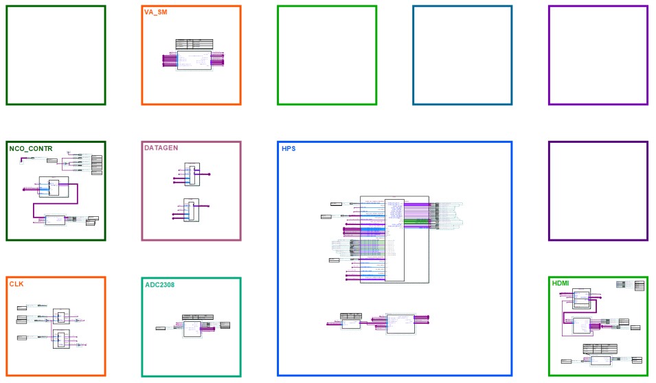
The appearance of the top-level file in the program Quartus II
After spending more than a couple of days off in the laboratory, we collected the entire system. It did not work for the entire potential frequency range, measured only the parameter S11, and on the monitor reflected the measured phase and amplitude characteristics of the connected device. The externally assembled device still didn’t look too attractive - three separate boards connected by single-conductor wiring, but this is a working prototype, and you can bring the marafet in the next step. We wrote the text, illustrated the stages of implementation, shot the video, downloaded everything to the site and waited.
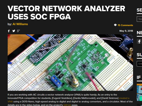
Of course, we sent links to these materials to some acquaintances in order to slightly add views. However, one day the views began to grow themselves, as if someone had poured it into promotion. After a little analysis, it turned out that our project was noticed on hackaday.io [7] and the overwhelming majority of the views were from there. It was interesting to see the first responses to our project. Inspired, we waited for the results.
This is not the first year of our participation in the competition. This project was for us the most thoughtful among the previously completed student work. But it did not grow together: we did not go to the next stage. Perhaps this is due to a misunderstanding between us and the judges. Perhaps just the project is not in the area of current trends for FPGA in full (cryptography, parallel computing, neural networks, etc.). But for us this is a big step in the development of SoC FPGA, a new branch of development and, most importantly, experience.
Congratulations to the Russian representatives, who took second place in the final competition!
I thank my colleagues in the project Danilu Nikiforovsky and Yevgeny Vostrikov and the leaders Ivan Deineka , Philip Shuklin and Artem Aleinik for their active participation and support.
[1] Innovate Europe 2015 Contest www.innovateeurope.org/eu/2015winner.html
[2] An Engineer's Guide to the High-Speed Interface, Jose Moreira, Hubert Wekmann, 2010, Appendix F, p. 503
[3] Spectrum a periodic sequence of rectangular pulses, ru.dsplib.org/content/fourier_series_pimp/fourier_series_pimp.html
[4] Zurich Instruments www.zhinst.com/applications/principles-of-lock- in-detection
[5] Low-frequency circulator / insulator without ferrite and magnet www.cqham.ru/oth9.htm
[6] VAC project for DE10-Nano board github.com/tvShushtov/em078_vector_analyzer
[7] VAC article on Hackadayhackaday.com/2018/05/09/vector-network-analyzer-uses-soc-fpga
Introduction
It was October 2017, I did a weekly routine check: an analysis of ongoing conferences on topics that are implemented in our department. At one point, I receive a mailing list from Terasic: a new competition for developing projects using debug boards on FPGA , now worldwide, starts . The experience of the same contest of last year rushes and comes to mind: postponing the month to the last two weeks, long debugging and tuning of the algorithms and issuing all channels to the monitor and promising not to postpone it anymore to the last day.
It was a great experience, during which we learned a lot about such a platform as SoC FPGA - the union between a huge array of logic elements and the Cortex-A9 processor, as well as their interaction with each other and with the periphery on the debug board.
New competition - new rules, new requirements, new level. Now the competition is held in several stages: first, the regional stages are held, and then the final in San Jose; All participants are sent the same fee, the DE10-Nano , and in addition you can now choose not only the basic three modules, but also a large version of the Analog Devices boards! However, unlike contests in previous years, this time it is necessary to sign a guarantee for the project, and in case of non-fulfillment, participants must send the fees back. Quite rightly, given the statistics of past years:
<...> 71 teams from 20 European countries registered the contest <...> 25 judges from Industry (ALTERA) and Academia (CNFM) in France reviewed the 32 projects [1].The supervisor as well as the students who wanted to be involved in this work was already under a heavy load on various projects, but the excitement during the competition and the motivation to learn many new things became weighty arguments to again take part in the competition. It remained to come up with a project with which you can apply.
Idea for the project
To ensure that the project did not stand aside, it was decided to implement a device useful for the department, which then can be easily refined and improved. Based on the department's areas of activity, there were various options: optical reflectometer, stroboscopic oscilloscope, etc. Quickly reviewing already existing applications and available additional fees, it was revealed that the reflectometer was already stated, and a stroboscopic oscilloscope was not assembled on such elements. The only idea remained tenacious - vector network analyzer. The other day, a pair of coils was brought to the laboratory, for which there was no documentation. The task was to determine at least the approximate characteristics of these coils. It was known that they assembled an oscillatory circuit, so the main task was to find out the resonant frequency. In such tasks, a vector network analyzer (VAC or VNA - Vector Network Analyzer) can be used. VNA allows you to define a scattering matrix, also known as an S-parameter matrix. In this method, the element under study is considered as a black box, which analyzes the incident and reflected signals from the ports of this device. So, for a dual-port system, the matrix is as follows:

Where V1 + V2 + - electromagnetic waves arriving at the ports;
V1- V2– are electromagnetic waves emerging from the ports;
Sij - elements of the multipole scattering matrix. [2]
Scheme for measuring S-parameters of a multipole
The components and circuit could not be examined with X-rays (at least with metro X-rays), so the following scheme was assembled on the knees: frequencies were circulated to the coil input using a generator, the second port of the circulator was connected to the coil input, and the third input on the oscilloscope, which has in its software mode amplitude-frequency analysis. Such a scheme allows to measure the parameter S11, i.e. reflection. In the end, after long suffering and calibrations, it was possible to remove this characteristic - but at what price? The department had long anticipated the acquisition of a vector network analyzer for such tasks (measurements of the AFC of electronic devices), but this purchase was always somehow postponed.
After messing around with the coils, it was decided to assemble our own network analyzer with visualization and comfortable tuning. It’s easy to find the excitement and desire to learn something new for students and postgraduates working at the department, so the team was quickly assembled from an electronics engineer, a programmer on the chip, me and two mentors.
No sooner said than done! After numerous discussions about the frequency band, processing algorithms and other parameters of the project, the application contained the following:
- The proposed project is a vector network analyzer based on SoC FPGA on the DE10-Nano;
- Requested additional fees: a board with a programmable frequency generator, a high-frequency mixer and a board with ADC;
- Operating frequency range: according to the presented options for additional cards;
- The possibility of rapid expansion of the number of connected ports;
- Output the amplitude and phase components on the screen;
- Other basic input / output functions for a vector network analyzer.
To pass to the next stage, it was necessary for the project page to garner a sufficient number of “likes” from users registered on the site. At first, everything went well, but then some dubious projects began to gain unrealistic and contrasting values of likes and views compared to other projects. It turned out that the competition site was too vulnerable to cheating.
After some time, the organizers announced that the board of judges would still choose the finalists, so the likes of the users, in fact, lost their weight. On January 31, our team appeared in the lists of those passing to the next stage, and we began to think over our project in more detail in anticipation of debugging.
Harsh reality
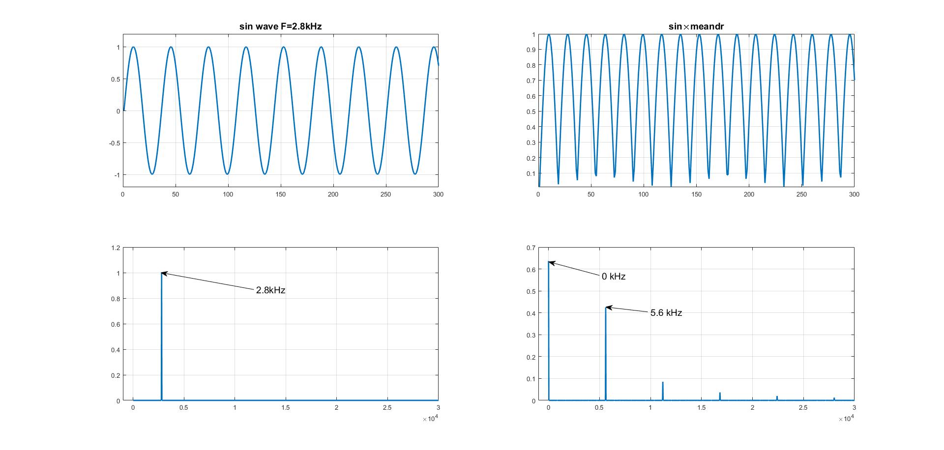
First came the DE10-Nano board. Nice, but a bit strange: expect that the boards will come all together. A few days later, a call comes in from customs: the fees came, they all together exceed the threshold for the price, so you need to pay an amount approximately equal to the cost of these fees for customs clearance. Such a deal disappointed us, but did not suit us: we refused the boards. In the presence of mixers and generators, we did not have, it is necessary to find new solutions. What to do? The first thing that came to my head was not the most accurate, but rather unusual solution: use the regular GPIO leg and generate a square wave from it. At the output of this leg, an analog low-pass filter is installed with a cut-off band slightly larger than the maximum frequency of the square wave. To start the analysis, it was suggested to start with 1 MHz (for example): then after the filter we would get a more or less pure sine (the higher harmonics would be cut off by the filter), and so on until the frequency drops to the one where there will be two harmonics in the signal after the filter. The meander is the sum of odd harmonics, and the proportional contribution of each harmonic is known in advance [3].
An example of the meander in the time and frequency domains: the spectrum shows the components of the harmonic signal at 500 kHz, 1.5 MHz, etc.
With a filter with a cut-off frequency of 1 MHz, you can go down to 33. (3) kHz. After this frequency for the filter, we should get the sum of two sines. The proportional ratio of their amplitudes is known (sinc-function), the response of the measured device to a frequency of 1 MHz (the first odd harmonic) also means that it remains for us to make an equation with one unknown and calculate the response characteristic at a frequency of 33, (3) kHz! At first, this solution seemed too simple, so for the beginning it was told to everyone in the hope that someone would find a mistake. No errors were found, but as the discussion proceeded, a number of restrictions were discovered:
- The GPIO leg is not the best source of the meander, especially with increasing frequency;
- Soldering a compact filter on the available components will be a non-trivial task;
- Even if these limitations can be circumvented, there is a synchronization problem for phase detection.
Suppose we have solved all the problems on the analog part; programmatically, there are two others:
- With decreasing frequency, the error of each previous detection and calculation will contribute to the subsequent measurement;
- With decreasing frequency, the time to calculate the characteristics will increase significantly.
And finally, last but not least. The described scheme can be used if the measured element can be described by a linear transfer function. However, if we measure the black box with non-linear characteristics, there are more problems than ideas from the idea. There was not much time left (the first result should be shown two months after the arrival of the board), so after a brief reflection we decided to double-check our reserves on the debug boards already available - and found a 14-bit DAC at 125 Msps ! Not the most elegant solution, but you don’t have to choose, we use it as an output signal generator.
First concept
The selected DAC as a generator accepts data at the input of the parallel bus and latches it with a clock signal coming from the FPGA. Such a scheme is ideal for synchronization in our scheme. However, with the detection remained questions.
Yes, there is a 14-bit 65 Msps ADC on the same board. But here the potential of the generator is potentially higher, and according to Kotelnikov's theorem, this ADC will no longer work at maximum frequencies.
The solution was found during the discussion of this problem with experienced electronics engineers. It turned out that for our task we can use a synchronous detector circuit (lock-in amplifier): the output of such a detector are two constant values, the phase and quadrature components, from which the amplitude and phase of the signal can be obtained, and since they are constant, they can be detected even with the slow ADC installed on the DE10-Nano! It was decided to first model the circuit in LTSpice, and then select the components and assemble the circuit, taking into account that the detector input is a signal from the circulator, and the outputs are connected to the ADC on the DE10-Nano board.
About synchronous detector and circulator
Синхронный детектор применяется и в цифровой обработке сигналов для детектирования различных сигналов на фоне шумов. Хорошее описание есть у Zurich Instruments [4], в нашем случае детектирование производится следующим образом: отраженный сигнал известной частоты умножается на меандр с использованием высокочастотного переключателя и операционного усилителя:
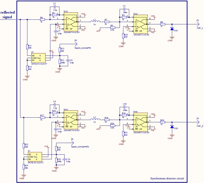
Схема детектирования отраженного сигнала
На деле умножение реализовано как переключение режима работы операционного усилителя, а переключение управляется двумя меандрами, поступающих с платы DE10-Nano: один из них в фазе с исходным сигналом (поступающим на вход устройства), а другой с задержкой по фазе на 90 градусов.
Результатом умножения становится перенос полезного сигнала в постоянную составляющую, а все частоты выше уже не интересны и поэтому могут быть отфильтрованы:
Спектр сигнала до и после умножения: на выходе операционного усилителя можно собрать простой ФНЧ для выделения только постоянной составляющей
Циркулятор на операционных усилителях (ОУ) представляет собой схему последовательного соединения операционных усилителей, замкнутых в кольцо. Циркуляторы на ОУ применяются для многих целей, в частности, для настройки антенн, усилителей, генераторов, гигабитный Ethernet и т.п. в диапазоне частот до сотен мегагерц. При создании ВАЦ использовалась схема циркулятора, созданная на основе двух операционных усилителей [5].
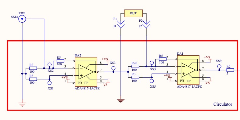
Схема циркулятора для подключения измеряемого устройства
Схема детектирования отраженного сигнала
На деле умножение реализовано как переключение режима работы операционного усилителя, а переключение управляется двумя меандрами, поступающих с платы DE10-Nano: один из них в фазе с исходным сигналом (поступающим на вход устройства), а другой с задержкой по фазе на 90 градусов.
Результатом умножения становится перенос полезного сигнала в постоянную составляющую, а все частоты выше уже не интересны и поэтому могут быть отфильтрованы:
Спектр сигнала до и после умножения: на выходе операционного усилителя можно собрать простой ФНЧ для выделения только постоянной составляющей
Циркулятор на операционных усилителях (ОУ) представляет собой схему последовательного соединения операционных усилителей, замкнутых в кольцо. Циркуляторы на ОУ применяются для многих целей, в частности, для настройки антенн, усилителей, генераторов, гигабитный Ethernet и т.п. в диапазоне частот до сотен мегагерц. При создании ВАЦ использовалась схема циркулятора, созданная на основе двух операционных усилителей [5].
Схема циркулятора для подключения измеряемого устройства
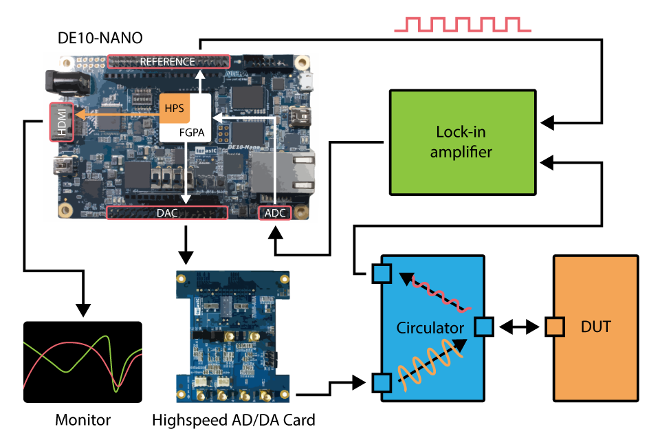
Updated design concept
Sinusoidal signals with a frequency of 1 Hz to 1 MHz with steps of a few Hz sent to the first port of the circulator. The device under study was connected to the second port, depending on the frequency response of which the signal reflectance changed. The reflected signal arrived at port 3, where a synchronous detector circuit was assembled to determine the frequency and phase characteristics. For correct operation, the ports of the circulator were adapted for a 100 Ohm impedance, which was associated with the output resistance of the D / A converter and the choice of the devices under study.
Less than a month remained before the project was completed, and by the end of the term it was necessary to also prepare reporting materials: a detailed description of the project on the contest page, a project posted on GitHub in the public domain and a video report on the work done.
Since we now understood what data would be fed into the inputs and outputs, we began work on a project for SoC FPGA. We saw the project being implemented as follows: the user sets the frequency range in which the measurement is planned, the FPGA begins to generate harmonics in the specified interval in turn using a DAC, the ADC accepts quadrature and phase components at the input, converting them into the amplitude and phase values at the current frequency , the values obtained are displayed in real time on a monitor connected to the debug board. There had already been some groundwork on displaying information on the monitor, so the main part was to correctly draw the data in real time and display the picture on HDMI. We ungrouped. The first group took up tasks for the program for the processor, deal more with the necessary initializations, data visualization issues. We also asked them to raise the screen resolution to 1024x768 [6]. The second group contains details on the implementation of the part on the FPGA, which should then be brought to the processor via the lightweight_h2f interface bus, as well as testing the performance of the first prototype of the synchronous detector. After eliminating the shortcomings and successfully measuring the characteristics of several elements, there was little time left, so the next two days were devoted to connecting the systems together, adding reports and mounting the video. which should then be brought to the processor via the lightweight_h2f interface bus, as well as testing the performance of the first prototype of the synchronous detector. After eliminating the shortcomings and successfully measuring the characteristics of several elements, there was little time left, so the next two days were devoted to connecting the systems together, adding reports and mounting the video. which should then be brought to the processor via the lightweight_h2f interface bus, as well as testing the performance of the first prototype of the synchronous detector. After eliminating the shortcomings and successfully measuring the characteristics of several elements, there was little time left, so the next two days were devoted to connecting the systems together, adding reports and mounting the video.
The appearance of the top-level file in the program Quartus II
Last minutes
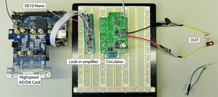
After spending more than a couple of days off in the laboratory, we collected the entire system. It did not work for the entire potential frequency range, measured only the parameter S11, and on the monitor reflected the measured phase and amplitude characteristics of the connected device. The externally assembled device still didn’t look too attractive - three separate boards connected by single-conductor wiring, but this is a working prototype, and you can bring the marafet in the next step. We wrote the text, illustrated the stages of implementation, shot the video, downloaded everything to the site and waited.
Of course, we sent links to these materials to some acquaintances in order to slightly add views. However, one day the views began to grow themselves, as if someone had poured it into promotion. After a little analysis, it turned out that our project was noticed on hackaday.io [7] and the overwhelming majority of the views were from there. It was interesting to see the first responses to our project. Inspired, we waited for the results.
but
This is not the first year of our participation in the competition. This project was for us the most thoughtful among the previously completed student work. But it did not grow together: we did not go to the next stage. Perhaps this is due to a misunderstanding between us and the judges. Perhaps just the project is not in the area of current trends for FPGA in full (cryptography, parallel computing, neural networks, etc.). But for us this is a big step in the development of SoC FPGA, a new branch of development and, most importantly, experience.
Ps
Congratulations to the Russian representatives, who took second place in the final competition!
I thank my colleagues in the project Danilu Nikiforovsky and Yevgeny Vostrikov and the leaders Ivan Deineka , Philip Shuklin and Artem Aleinik for their active participation and support.
Links
[1] Innovate Europe 2015 Contest www.innovateeurope.org/eu/2015winner.html
[2] An Engineer's Guide to the High-Speed Interface, Jose Moreira, Hubert Wekmann, 2010, Appendix F, p. 503
[3] Spectrum a periodic sequence of rectangular pulses, ru.dsplib.org/content/fourier_series_pimp/fourier_series_pimp.html
[4] Zurich Instruments www.zhinst.com/applications/principles-of-lock- in-detection
[5] Low-frequency circulator / insulator without ferrite and magnet www.cqham.ru/oth9.htm
[6] VAC project for DE10-Nano board github.com/tvShushtov/em078_vector_analyzer
[7] VAC article on Hackadayhackaday.com/2018/05/09/vector-network-analyzer-uses-soc-fpga