Design standards in microelectronics: where are actually 7 nanometers in 7 nm technology?
Modern microelectronic technologies - like "Ten Little Indians". The cost of development and equipment is so high that with each new step forward someone falls off. After the news about the refusal of GlobalFoundries to develop 7 nm, there are three of them: TSMC, Intel and Samsung. And what is the “design norms” proper and where is that coveted size of 7 nm? And is he there at all?
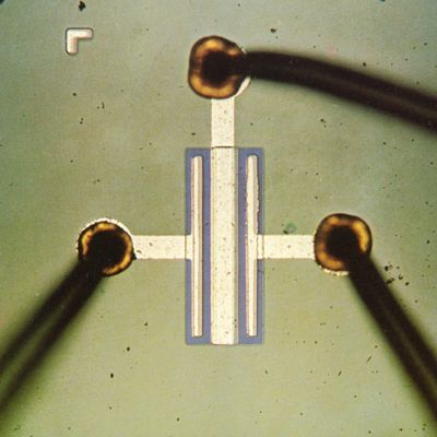
Figure 1. Fairchild FI-100 Transistor, 1964.
The very first serial MOSFETs entered the market in 1964 and, as sophisticated readers can see from the figure, they almost did not differ from the more or less modern ones - except for size (look at the wire for scale).
Why reduce the size of transistors? The most obvious answer to this question is called Moore's law and says that every two years the number of transistors on a chip should be doubled, which means that the linear dimensions of transistors should decrease by a factor of two. "Must" - according to the observations of Gordon Moore (and some other engineers) in the seventies. Moore’s law implies many other factors that make up the ITRS microelectronics roadmap. The simplest and coarsest formulation of Moore’s law implementation methods (also known as Dennard’s law of miniaturization) —the increase in the number of transistors on a chip should not lead to an increase in power density, that is, as the size of the transistors decreases, the supply voltage and operating current should be proportionally reduced.
The current through the MOS transistor is proportional to the ratio of its width to length, which means we can keep the same current proportionally decreasing both of these parameters. Moreover, reducing the size of the transistor, we also reduce the gate capacitance (proportional to the product of the length and width of the channel), making the circuit even faster. In general, in the digital circuit there is almost no reason to make the transistors larger than the minimum allowable size. Then begin the nuances about the fact that in logic, p-channel transistors are usually somewhat wider than n-channel to compensate for the difference in charge carrier mobility, and in memory, on the contrary, n-channel transistors are wider so that the memory is normally recorded using a non-complementary key, but this is really nuances, and globally - the smaller the size of the transistor - the better for digital circuits.
That is why the channel length has always been the smallest size in the topology of the chip, and the most logical designation of design standards.
Here it should be noted that the above reasoning about the size is not valid for analog circuits. For example, right now on the second monitor of my computer there is a matched pair of transistors for 150 nm technology, 32 pieces each 8/1 microns in size. This is done in order to ensure the identity of these two transistors, despite the technological variation of parameters. The area is of secondary importance.
Technologists and topologists have a so-called lambda system of typical topology dimensions. It is very convenient for studying design (and was invented at the University of Berkeley, if I am not mistaken) and transfer designs from factory to factory. In fact, this is a generalization of typical sizes and technological limitations, but a bit rude so that it can work out in any factory. On her example, it is convenient to look at the typical dimensions of the elements in the chip. The principles at the heart of the lambda system are very simple:
From the third point it follows, in particular, that lambda in old technologies is half of the design standard (more precisely, the length of the transistor channel and the design standards are two lambda).
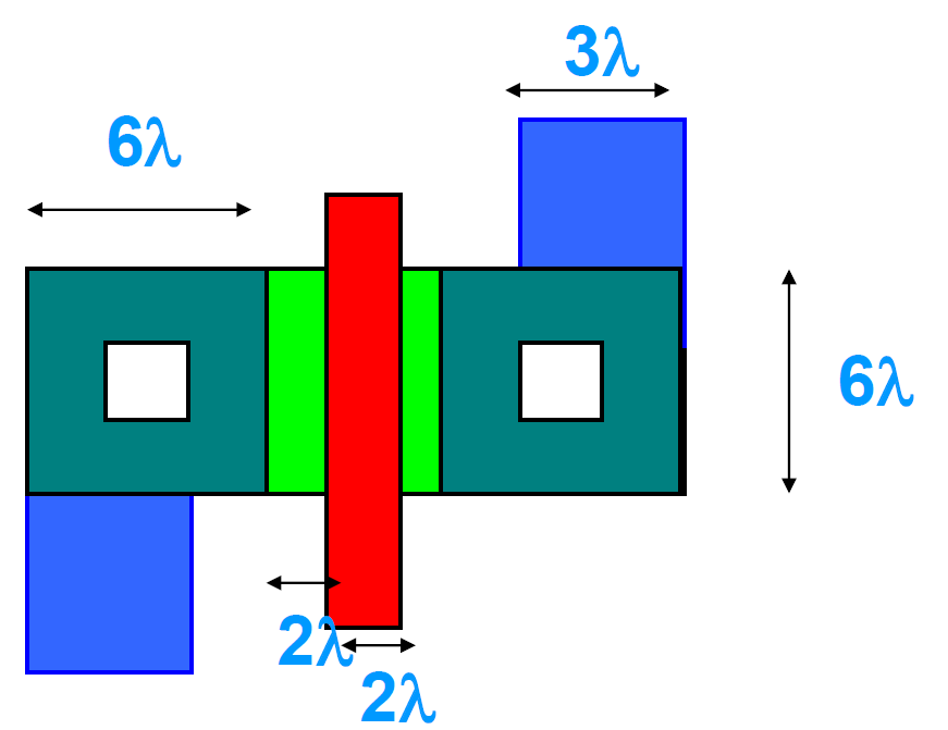
Figure 2. An example of a topology performed on a lambda system.
The lambda system worked perfectly on the old design standards, allowing you to conveniently transfer production from the factory to the factory, organize second chip suppliers and do a lot more of what is useful. But with increasing competition and the number of transistors on a chip, factories began to strive to make the topology a little more compact, so now the design rules corresponding to the “pure” lambda system cannot be found, except in situations where developers independently chop them off, bearing in mind the probability of production chip in different factories. However, over the years, the industry has developed a direct link “design norms = transistor channel length”, which successfully existed until the sizes of transistors reached tens of nanometers.
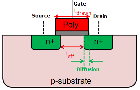
Figure 3. Schematic section of the transistor.
This figure shows a VERY greatly simplified section of a conventional planar (flat) transistor, showing the difference between the topological channel length (Ldrawn) and the effective channel length (Leff). Where does the difference come from?
Speaking of microelectronic technology, photolithography is almost always mentioned, but much less often - other, no less important technological operations: etching, ion implantation, diffusion, etc. etc. For our conversation with you, it would not be superfluous to remind you how diffusion and ion implantation work.
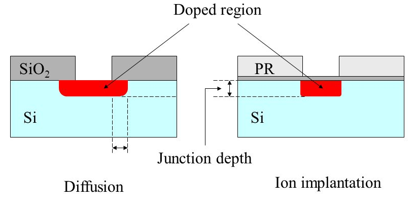
Figure 4. Comparison of diffusion and ion implantation.
Diffusion is simple. You take a silicon wafer, on which in advance (with the help of photolithography) a drawing is applied that covers the places where an admixture is not needed and opens those where it is needed. Next you need to put a gaseous impurity in one chamber with a crystal and heat to a temperature at which the impurity will penetrate into the silicon. By adjusting the temperature and duration of the process, you can achieve the required amount and depth of the impurity.
The obvious minus of diffusion is that the impurity penetrates into silicon in all directions equally, which is down and sideways, thus reducing the effective length of the channel. And we are talking now about hundreds of nanometers! While the design standards were measured in tens of microns, everything was fine, but of course, this state of affairs could not last for a long time, and ion implantation replaced the diffusion.
During ion implantation, a beam of impurity ions is accelerated and directed to a silicon wafer. In this case, all the ions move in one direction, which practically excludes their spreading to the sides. In theory, of course. In practice, the ions still crawl a little to the sides, albeit at much smaller distances than during diffusion.
However, if we return to the figure of the transistor, we will see that the difference between the topological and effective length of the channel begins precisely because of this small spread. She, in principle, could be neglected, but she is not the only reason for the difference. There are still short channel effects. There are five of them, and they change the parameters of the transistor in different ways if the length of the channel approaches different physical limitations. I will not describe all of them, I’ll dwell on the most relevant for us - DIBL (Drain-Induced Barrier Lowering, drain-induced lowering of potential barrier).
In order to get into the drain, the electron (or hole) must overcome the potential barrier of the stock pn junction. The voltage on the gate reduces this barrier, thus controlling the current through the transistor, and we want the gate voltage to be the only control voltage. Unfortunately, if the transistor channel is too short, the drain pn-junction begins to influence the transistor behavior, which, firstly, reduces the voltage threshold (see figure below), and secondly, the voltage through the transistor does not affect only the gate , but also on the drain, because the thickness of the stock pn junction increases in proportion to the voltage on the drain and accordingly shortens the channel.
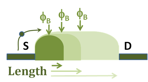
Figure 5. Drain-Induced Barrier Lowering Effect (DIBL).
Source - Wikipedia.
In addition, reducing the channel length leads to the fact that charge carriers begin to freely fall from the source into the drain, bypassing the channel and forming a leakage current (bad current in the figure below), which is also static power consumption, the absence of which was one of the important reasons for the early success of CMOS -technology, rather inhibitory in comparison with the bipolar competitors of the time. In fact, each transistor in modern technology has a resistor parallel to it, the nominal of which is smaller, the shorter the channel length.
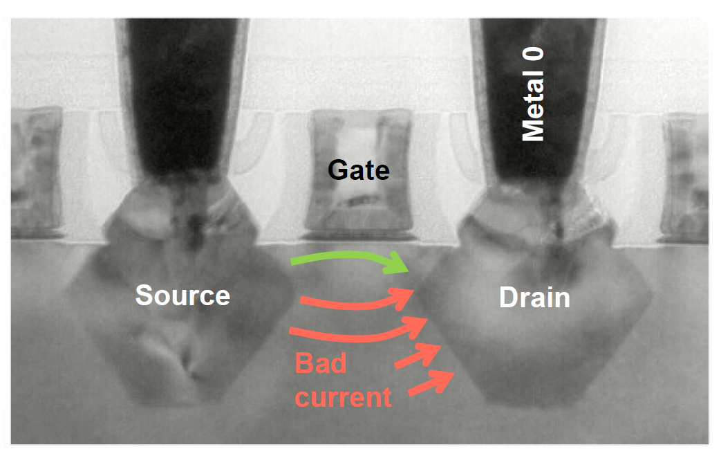
Figure 6. Static consumption growth due to leaks in short-channel technologies.
Source - Synopsys.
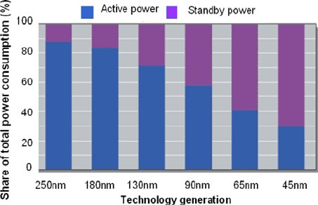
Figure 7. The share of static energy consumption of microprocessors at different design standards.
Source - B. Dieny et. al., "Spin-Transfer Effect", International Journal of Nanotechnology, 2010
Now, as you can see in the figure above, static consumption is much higher than dynamic and is an important obstacle to creating low-power chips, for example, wearable electronics and the internet of things. Actually, at about the moment when it became an important problem, marketing marketing began with design standards, because progress in lithography began to outpace progress in physics.
To combat the undesirable effects of a short channel on design standards of 800-32 nanometers, many different technological solutions were invented, and I will not describe them all, otherwise the article will grow to a very indecent size, but with each new step I had to introduce new solutions - additional doping areas adjacent to pn junctions, doping in depth to prevent leaks, local transformation of silicon in transistors into silicon-germanium ... Not a single step in reducing the size of transistors was easy oh so
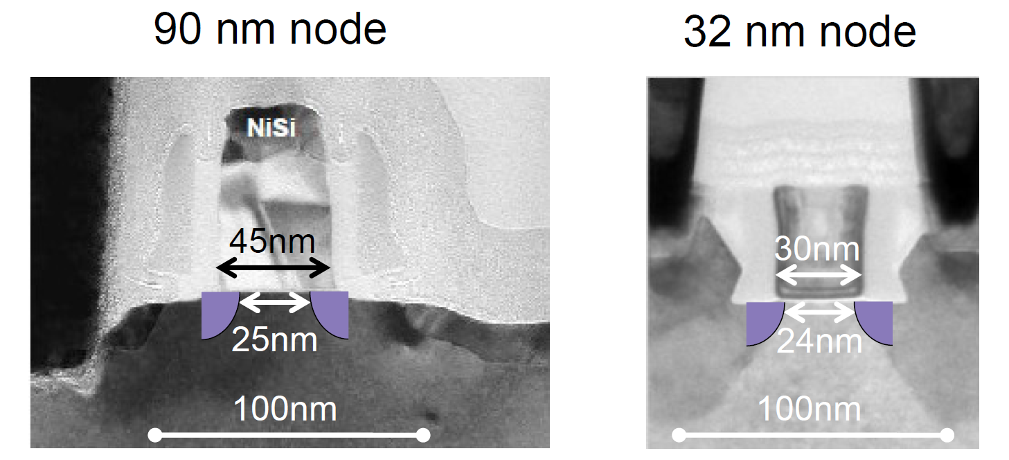
Figure 8. The effective channel length in the 90 nm and 32 nm technologies. Transistors are shot at the same scale. The semicircles in the figures are a form of additional weak drainage adjustment (LDD, lightly doped drain) made to reduce the width of the pn junctions.
Source - Synopsys.
Typical dimensions of metallization and the distance between elements during the transition from 90 nm to about 28 nm decreased in proportion to the decrease in design standards, that is, the typical size of the next generation was 0.7 from the previous one (to obtain a two-fold reduction in area according to Moore's law). At the same time, the channel length decreased at best as 0.9 from the previous generation, and the effective channel length practically did not change at all. It is clearly seen from the figure above that the linear dimensions of the transistors did not change by a factor of three when going from 90 nm to 32 nm, and all the technologists' games were around reducing gate overlaps and doped areas, as well as around monitoring for static leaks, which did not allow the channel is shorter.
As a result, two things became clear:
Moore's law is generally a controversial topic, because it is not a law of nature, but an empirical observation of certain facts from the history of one particular company, extrapolated to the future progress of the entire industry. Actually, the popularity of Moore's law is inextricably linked with Intel marketers, who made it their banner and, in fact, for many years pushed the industry forward, forcing it to comply with Moore's law, where it might be worth the wait.
What is the way out of marketers? Very elegant.
The length of the transistor channel is good, but how can we estimate the area gain, which gives the transition to new design standards? For a long time in the industry, the area of a six-transistor memory cell, the most popular building block of microprocessors, was used for this. It is from these cells that the cache memory and the register file that can occupy a half-crystal usually consist, and that is why the six-transistor cell layout and topology are always carefully licked to the limit (often special people who do just that), so this is really a good measure packing density.
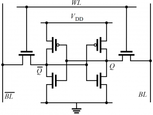
Figure 9. Diagram of a six-transistor static memory cell.
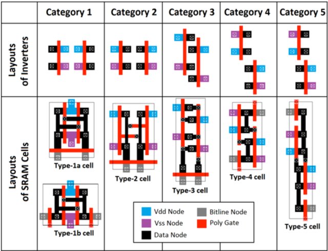
Figure 10. Different topology options for a six-cell static memory cell. Source - G. Apostolidis et. al., “Design and Simulation of 6T SRAM Cell Architectures in 32nm Technology”, Journal of Engineering Science and Technology Review, 2016
So for a long time in descriptions of technology, the figure of design standards was accompanied by the second figure - the area of the memory cell, which, in theory, should be derived from the length of the channel. And then there was an interesting substitution of concepts. At the moment when direct scaling stopped working, and the channel length ceased to decrease every two years according to Moore's law, marketers guessed that it was possible not to deduce the area of the memory cell from the design norms, but to deduce the figure of the design norms from the area of the memory cell!
That is, naturally, “before, we had a channel length of 65 nm and a memory cell area of X, and now the channel length is 54 nm, but we have stung the metallization, and now the cell area is X / 5, which roughly corresponds to the transition from 65 to 28 nm. So let's say to everyone that we have 28nm design norms, and we’re not going to tell anyone about the 54nm channel length? ”In fairness,“ stung metallization ”is also an important achievement, and some time after the start of problems with the miniaturization of the transistors themselves The minimum width of the metallization, the size of the contact to the transistor, or some other figure on the topology corresponded to the design standards voiced. But then dances with FinFET transistors began, in which the key dimensions are in no way connected with the resolution of lithography, the speed of miniaturization of the transistors and everything else finally diverged,
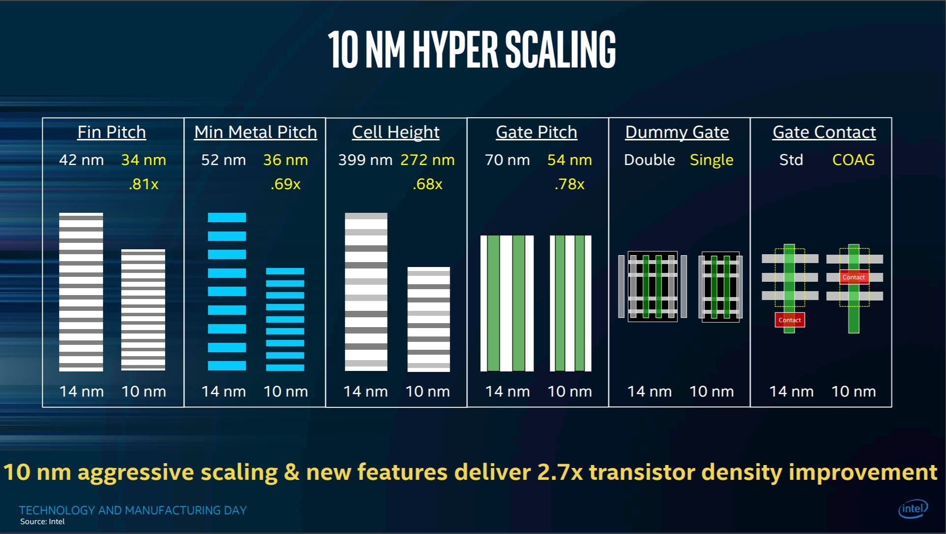
Figure 11. Comparison of 14nm and 10nm Intel technologies.
The source is Intel.
Here is a great example of this “new scaling”. We are shown how the characteristic dimensions in the memory cell have changed. Many parameters, but not a word about the length and width of the transistor channel!
How did the technologists solve the problem of the impossibility of reducing the length of the channel and controlling leakage?
They found two ways. The first is head-on: if the cause of the leaks is a large depth of implantation, let's reduce it, preferably radically. The “silicon on insulator” (SOI) technology has been known for a very long time (and it has been actively used all these years, for example, in 130-32 nm AMD processors, 90 nm processor of the Sony Playstation 3, and also in radio frequency, power or space electronics), but with a decrease in design standards, she received a second wind.

Figure 12. Comparison of transistors made using conventional volume and FDSOI (fully depleted SOI) technologies.
Source - ST Microelectronics .
As you can see, the idea is more than elegant - under a very thin active layer is oxide, which removes the harmful leakage current on the vine! At the same time, by reducing the capacity of the pn junctions (four of the five sides of the drain cube were removed), the speed is increased and power consumption is still reduced. That is why now FDSOI 28-22-20 nm technologies are actively advertised as platforms for IoT chips - consumption is indeed decreasing by several times, if not an order of magnitude. And yet this approach allows in the future to glue an ordinary flat transistor to the level of 14–16 nm, which the volumetric technology will not allow.
Nevertheless, FDSOI doesn’t especially fall below 14 nm, and the technology also has other problems (for example, the terrible high cost of SOI substrates), and therefore the industry has come to another solution - FinFET transistors. The idea of a FinFET transistor is also quite elegant. Do we want most of the space between the drain and the source to be controlled by the shutter? So let's surround this space with a shutter on all sides! Well, not all, three will be enough.
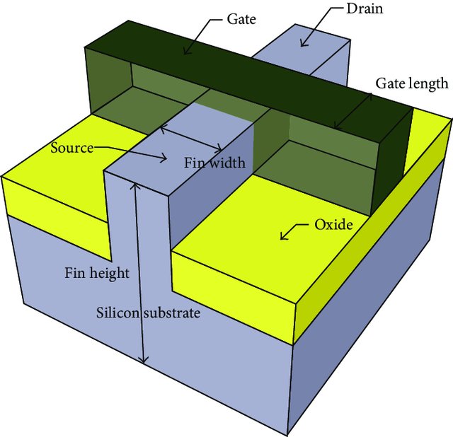
Figure 13. FinFET structure.
Source - A. Tahrim et.al., “Design and Performance Analysis of 1-Bit FinFET Full Adder Cells for Subthreshold Region at 16 nm Process Technology”, Journal of Nanomaterials, 2015
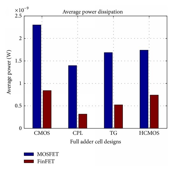
Figure 14. Comparison of power consumption of different variants of the adder, performed on planar transistors and FinFET.
Source - A. Tahrim et.al., “Design and Performance Analysis of 1-Bit FinFET Cement for Subthreshold Region at 16 nm Process Technology”, Journal of Nanomaterials, 2015
In FinFET, the channel is not flat and located directly below the substrate surface, and it forms a vertical fin (Fin - this is a fin), protruding above the surface and surrounded on three sides by a shutter. Thus, the entire space between the drain and the source is controlled by the shutter, and the static leakage is greatly reduced. The first FinFET serially released by Intel at the design standards of 22 nm, then the rest of the top manufacturers, including such a SOI apologist as Global Foundries (former AMD), were pulled up.
The channel verticality in FinFET, among other things, allows saving on cell space, because FinFET with a wide channel is rather narrow in projection, and this, in turn, again helped marketers with their stories about the memory cell area and its two-fold decrease with each new step "design standards", not in any way tied to the physical size of the transistor.
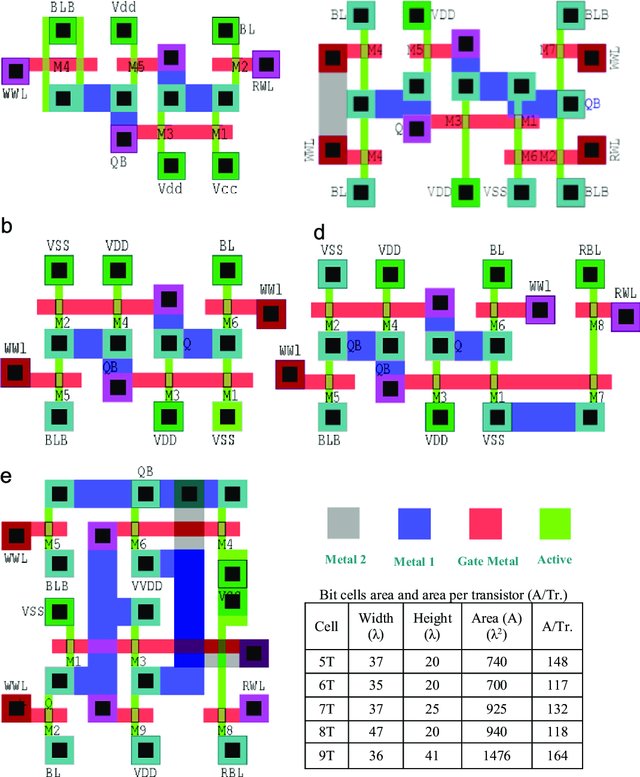
Figure 15. Topologies of different memory cell variants (5T-9T) in technology with FinFET. Source - M. Ansari et. al., “FinMET technologies”, the VLSI Journal on Integration, Volume 50, June 2015.
Here are some examples of different memory cells in the technology. with FinFET. See how the geometric width of the channel is much smaller than the length? It can also be seen that, despite all the perturbations, the topology lambda system is still used for quantitative estimates. And what about absolute numbers?
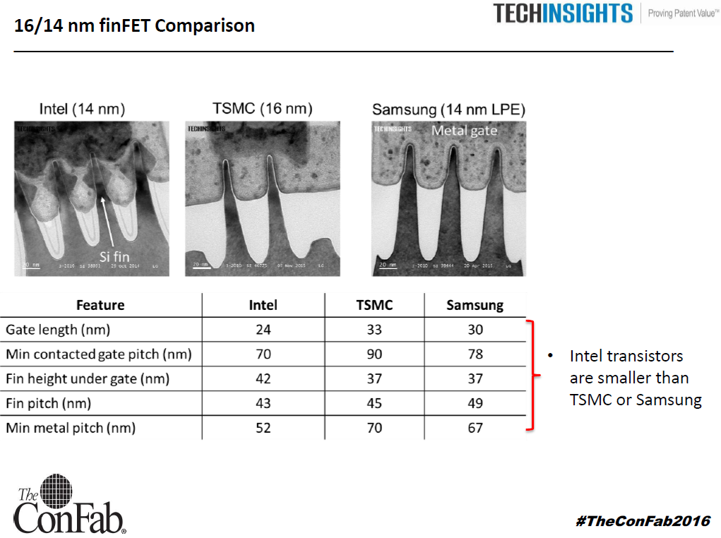
Figure 16. Some transistor sizes in 14-16 nm technologies.
Source - the ConFab 2016 conference.
As can be seen from the figure, the topological length of the channel in 16 nm FinFET technology is still more than 20-25 nm, as mentioned above. And this is logical, because physics can not be fooled. But from the same figure, you can make another, more interesting conclusion: if you look closely, it becomes clear that the minimum size available in transistors is not the length of the channel, but the width of the fin. And here we are in for an amusing discovery: the fin width in the Intel process technology is 16 nm (drum roll!) EIGHT nanometers.
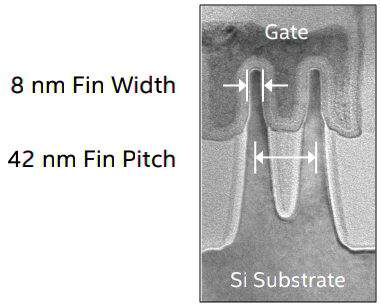
Figure 17. Fin dimensions in the 14nm Intel process technology.
Source - wikichip.org
As you can see, marketers, tied to the size of the memory cell, have deceived themselves, and now they are forced to voice the number more than they could. In fact, of course, in the conditions of a fundamental change in the structure of the transistor and the expectations of users to hear some kind of metric, the use of a metric reflecting the packing density was probably the only right decision, and marketers were ultimately right, although this sometimes leads to funny situations when the same design standards in different companies are called differently. For example, reading the news that TSMC has already launched 7 nm, and Intel is again delaying the start of production of 10 nm, it is worth remembering that 7 nm TSMC and 10 nm Intel are actually the same design standards in terms of and packing density, and the size of individual transistors.
What's next? In fact, nobody knows. Moore's law had exhausted itself for quite a long time, and ten years ago the answer to the question “what's next?” Could be found in the reports of research centers, now it is increasingly heard that promising developments have to be abandoned, as they turn out to be overly complex. in the implementation. This has already happened with the plates with a diameter of 450 millimeters, this is partly the case with EUV-lithography (with which scientists have been wearing for about twenty years), this will probably happen with transistors on graphene and carbon nanotubes. Another technological breakthrough is needed, but the path to it, sadly, is not yet visible. It got to the point that the new TSMC director Mark Liu calledthe most promising direction in the development of microelectronic technology is not a reduction in the size of transistors, but 3D integration. “Real” 3D integration, rather than combining several chips in a single package, will indeed be a huge milestone in the development of microelectronics, but Moore’s law, as the law of reducing the size of transistors, seems to have finally died.

Figure 1. Fairchild FI-100 Transistor, 1964.
The very first serial MOSFETs entered the market in 1964 and, as sophisticated readers can see from the figure, they almost did not differ from the more or less modern ones - except for size (look at the wire for scale).
Why reduce the size of transistors? The most obvious answer to this question is called Moore's law and says that every two years the number of transistors on a chip should be doubled, which means that the linear dimensions of transistors should decrease by a factor of two. "Must" - according to the observations of Gordon Moore (and some other engineers) in the seventies. Moore’s law implies many other factors that make up the ITRS microelectronics roadmap. The simplest and coarsest formulation of Moore’s law implementation methods (also known as Dennard’s law of miniaturization) —the increase in the number of transistors on a chip should not lead to an increase in power density, that is, as the size of the transistors decreases, the supply voltage and operating current should be proportionally reduced.
The current through the MOS transistor is proportional to the ratio of its width to length, which means we can keep the same current proportionally decreasing both of these parameters. Moreover, reducing the size of the transistor, we also reduce the gate capacitance (proportional to the product of the length and width of the channel), making the circuit even faster. In general, in the digital circuit there is almost no reason to make the transistors larger than the minimum allowable size. Then begin the nuances about the fact that in logic, p-channel transistors are usually somewhat wider than n-channel to compensate for the difference in charge carrier mobility, and in memory, on the contrary, n-channel transistors are wider so that the memory is normally recorded using a non-complementary key, but this is really nuances, and globally - the smaller the size of the transistor - the better for digital circuits.
That is why the channel length has always been the smallest size in the topology of the chip, and the most logical designation of design standards.
Here it should be noted that the above reasoning about the size is not valid for analog circuits. For example, right now on the second monitor of my computer there is a matched pair of transistors for 150 nm technology, 32 pieces each 8/1 microns in size. This is done in order to ensure the identity of these two transistors, despite the technological variation of parameters. The area is of secondary importance.
Technologists and topologists have a so-called lambda system of typical topology dimensions. It is very convenient for studying design (and was invented at the University of Berkeley, if I am not mistaken) and transfer designs from factory to factory. In fact, this is a generalization of typical sizes and technological limitations, but a bit rude so that it can work out in any factory. On her example, it is convenient to look at the typical dimensions of the elements in the chip. The principles at the heart of the lambda system are very simple:
- if the shift of elements on two different photolithographic masks has catastrophic consequences (for example, a short circuit), then the stock of sizes to prevent inconsistencies should be at least two lambda;
- if the shift of elements has undesirable, but not catastrophic consequences, the stock of sizes must be at least one lambda;
- The minimum size of the photomask window is two lambda.
From the third point it follows, in particular, that lambda in old technologies is half of the design standard (more precisely, the length of the transistor channel and the design standards are two lambda).

Figure 2. An example of a topology performed on a lambda system.
The lambda system worked perfectly on the old design standards, allowing you to conveniently transfer production from the factory to the factory, organize second chip suppliers and do a lot more of what is useful. But with increasing competition and the number of transistors on a chip, factories began to strive to make the topology a little more compact, so now the design rules corresponding to the “pure” lambda system cannot be found, except in situations where developers independently chop them off, bearing in mind the probability of production chip in different factories. However, over the years, the industry has developed a direct link “design norms = transistor channel length”, which successfully existed until the sizes of transistors reached tens of nanometers.

Figure 3. Schematic section of the transistor.
This figure shows a VERY greatly simplified section of a conventional planar (flat) transistor, showing the difference between the topological channel length (Ldrawn) and the effective channel length (Leff). Where does the difference come from?
Speaking of microelectronic technology, photolithography is almost always mentioned, but much less often - other, no less important technological operations: etching, ion implantation, diffusion, etc. etc. For our conversation with you, it would not be superfluous to remind you how diffusion and ion implantation work.

Figure 4. Comparison of diffusion and ion implantation.
Diffusion is simple. You take a silicon wafer, on which in advance (with the help of photolithography) a drawing is applied that covers the places where an admixture is not needed and opens those where it is needed. Next you need to put a gaseous impurity in one chamber with a crystal and heat to a temperature at which the impurity will penetrate into the silicon. By adjusting the temperature and duration of the process, you can achieve the required amount and depth of the impurity.
The obvious minus of diffusion is that the impurity penetrates into silicon in all directions equally, which is down and sideways, thus reducing the effective length of the channel. And we are talking now about hundreds of nanometers! While the design standards were measured in tens of microns, everything was fine, but of course, this state of affairs could not last for a long time, and ion implantation replaced the diffusion.
During ion implantation, a beam of impurity ions is accelerated and directed to a silicon wafer. In this case, all the ions move in one direction, which practically excludes their spreading to the sides. In theory, of course. In practice, the ions still crawl a little to the sides, albeit at much smaller distances than during diffusion.
However, if we return to the figure of the transistor, we will see that the difference between the topological and effective length of the channel begins precisely because of this small spread. She, in principle, could be neglected, but she is not the only reason for the difference. There are still short channel effects. There are five of them, and they change the parameters of the transistor in different ways if the length of the channel approaches different physical limitations. I will not describe all of them, I’ll dwell on the most relevant for us - DIBL (Drain-Induced Barrier Lowering, drain-induced lowering of potential barrier).
In order to get into the drain, the electron (or hole) must overcome the potential barrier of the stock pn junction. The voltage on the gate reduces this barrier, thus controlling the current through the transistor, and we want the gate voltage to be the only control voltage. Unfortunately, if the transistor channel is too short, the drain pn-junction begins to influence the transistor behavior, which, firstly, reduces the voltage threshold (see figure below), and secondly, the voltage through the transistor does not affect only the gate , but also on the drain, because the thickness of the stock pn junction increases in proportion to the voltage on the drain and accordingly shortens the channel.

Figure 5. Drain-Induced Barrier Lowering Effect (DIBL).
Source - Wikipedia.
In addition, reducing the channel length leads to the fact that charge carriers begin to freely fall from the source into the drain, bypassing the channel and forming a leakage current (bad current in the figure below), which is also static power consumption, the absence of which was one of the important reasons for the early success of CMOS -technology, rather inhibitory in comparison with the bipolar competitors of the time. In fact, each transistor in modern technology has a resistor parallel to it, the nominal of which is smaller, the shorter the channel length.

Figure 6. Static consumption growth due to leaks in short-channel technologies.
Source - Synopsys.

Figure 7. The share of static energy consumption of microprocessors at different design standards.
Source - B. Dieny et. al., "Spin-Transfer Effect", International Journal of Nanotechnology, 2010
Now, as you can see in the figure above, static consumption is much higher than dynamic and is an important obstacle to creating low-power chips, for example, wearable electronics and the internet of things. Actually, at about the moment when it became an important problem, marketing marketing began with design standards, because progress in lithography began to outpace progress in physics.
To combat the undesirable effects of a short channel on design standards of 800-32 nanometers, many different technological solutions were invented, and I will not describe them all, otherwise the article will grow to a very indecent size, but with each new step I had to introduce new solutions - additional doping areas adjacent to pn junctions, doping in depth to prevent leaks, local transformation of silicon in transistors into silicon-germanium ... Not a single step in reducing the size of transistors was easy oh so

Figure 8. The effective channel length in the 90 nm and 32 nm technologies. Transistors are shot at the same scale. The semicircles in the figures are a form of additional weak drainage adjustment (LDD, lightly doped drain) made to reduce the width of the pn junctions.
Source - Synopsys.
Typical dimensions of metallization and the distance between elements during the transition from 90 nm to about 28 nm decreased in proportion to the decrease in design standards, that is, the typical size of the next generation was 0.7 from the previous one (to obtain a two-fold reduction in area according to Moore's law). At the same time, the channel length decreased at best as 0.9 from the previous generation, and the effective channel length practically did not change at all. It is clearly seen from the figure above that the linear dimensions of the transistors did not change by a factor of three when going from 90 nm to 32 nm, and all the technologists' games were around reducing gate overlaps and doped areas, as well as around monitoring for static leaks, which did not allow the channel is shorter.
As a result, two things became clear:
- go below 25-20 nm without a technological breakthrough will not work;
- It has become increasingly difficult for marketers to paint a picture of how technological progress complies with Moore's law
Moore's law is generally a controversial topic, because it is not a law of nature, but an empirical observation of certain facts from the history of one particular company, extrapolated to the future progress of the entire industry. Actually, the popularity of Moore's law is inextricably linked with Intel marketers, who made it their banner and, in fact, for many years pushed the industry forward, forcing it to comply with Moore's law, where it might be worth the wait.
What is the way out of marketers? Very elegant.
The length of the transistor channel is good, but how can we estimate the area gain, which gives the transition to new design standards? For a long time in the industry, the area of a six-transistor memory cell, the most popular building block of microprocessors, was used for this. It is from these cells that the cache memory and the register file that can occupy a half-crystal usually consist, and that is why the six-transistor cell layout and topology are always carefully licked to the limit (often special people who do just that), so this is really a good measure packing density.

Figure 9. Diagram of a six-transistor static memory cell.

Figure 10. Different topology options for a six-cell static memory cell. Source - G. Apostolidis et. al., “Design and Simulation of 6T SRAM Cell Architectures in 32nm Technology”, Journal of Engineering Science and Technology Review, 2016
So for a long time in descriptions of technology, the figure of design standards was accompanied by the second figure - the area of the memory cell, which, in theory, should be derived from the length of the channel. And then there was an interesting substitution of concepts. At the moment when direct scaling stopped working, and the channel length ceased to decrease every two years according to Moore's law, marketers guessed that it was possible not to deduce the area of the memory cell from the design norms, but to deduce the figure of the design norms from the area of the memory cell!
That is, naturally, “before, we had a channel length of 65 nm and a memory cell area of X, and now the channel length is 54 nm, but we have stung the metallization, and now the cell area is X / 5, which roughly corresponds to the transition from 65 to 28 nm. So let's say to everyone that we have 28nm design norms, and we’re not going to tell anyone about the 54nm channel length? ”In fairness,“ stung metallization ”is also an important achievement, and some time after the start of problems with the miniaturization of the transistors themselves The minimum width of the metallization, the size of the contact to the transistor, or some other figure on the topology corresponded to the design standards voiced. But then dances with FinFET transistors began, in which the key dimensions are in no way connected with the resolution of lithography, the speed of miniaturization of the transistors and everything else finally diverged,

Figure 11. Comparison of 14nm and 10nm Intel technologies.
The source is Intel.
Here is a great example of this “new scaling”. We are shown how the characteristic dimensions in the memory cell have changed. Many parameters, but not a word about the length and width of the transistor channel!
How did the technologists solve the problem of the impossibility of reducing the length of the channel and controlling leakage?
They found two ways. The first is head-on: if the cause of the leaks is a large depth of implantation, let's reduce it, preferably radically. The “silicon on insulator” (SOI) technology has been known for a very long time (and it has been actively used all these years, for example, in 130-32 nm AMD processors, 90 nm processor of the Sony Playstation 3, and also in radio frequency, power or space electronics), but with a decrease in design standards, she received a second wind.

Figure 12. Comparison of transistors made using conventional volume and FDSOI (fully depleted SOI) technologies.
Source - ST Microelectronics .
As you can see, the idea is more than elegant - under a very thin active layer is oxide, which removes the harmful leakage current on the vine! At the same time, by reducing the capacity of the pn junctions (four of the five sides of the drain cube were removed), the speed is increased and power consumption is still reduced. That is why now FDSOI 28-22-20 nm technologies are actively advertised as platforms for IoT chips - consumption is indeed decreasing by several times, if not an order of magnitude. And yet this approach allows in the future to glue an ordinary flat transistor to the level of 14–16 nm, which the volumetric technology will not allow.
Nevertheless, FDSOI doesn’t especially fall below 14 nm, and the technology also has other problems (for example, the terrible high cost of SOI substrates), and therefore the industry has come to another solution - FinFET transistors. The idea of a FinFET transistor is also quite elegant. Do we want most of the space between the drain and the source to be controlled by the shutter? So let's surround this space with a shutter on all sides! Well, not all, three will be enough.

Figure 13. FinFET structure.
Source - A. Tahrim et.al., “Design and Performance Analysis of 1-Bit FinFET Full Adder Cells for Subthreshold Region at 16 nm Process Technology”, Journal of Nanomaterials, 2015

Figure 14. Comparison of power consumption of different variants of the adder, performed on planar transistors and FinFET.
Source - A. Tahrim et.al., “Design and Performance Analysis of 1-Bit FinFET Cement for Subthreshold Region at 16 nm Process Technology”, Journal of Nanomaterials, 2015
In FinFET, the channel is not flat and located directly below the substrate surface, and it forms a vertical fin (Fin - this is a fin), protruding above the surface and surrounded on three sides by a shutter. Thus, the entire space between the drain and the source is controlled by the shutter, and the static leakage is greatly reduced. The first FinFET serially released by Intel at the design standards of 22 nm, then the rest of the top manufacturers, including such a SOI apologist as Global Foundries (former AMD), were pulled up.
The channel verticality in FinFET, among other things, allows saving on cell space, because FinFET with a wide channel is rather narrow in projection, and this, in turn, again helped marketers with their stories about the memory cell area and its two-fold decrease with each new step "design standards", not in any way tied to the physical size of the transistor.

Figure 15. Topologies of different memory cell variants (5T-9T) in technology with FinFET. Source - M. Ansari et. al., “FinMET technologies”, the VLSI Journal on Integration, Volume 50, June 2015.
Here are some examples of different memory cells in the technology. with FinFET. See how the geometric width of the channel is much smaller than the length? It can also be seen that, despite all the perturbations, the topology lambda system is still used for quantitative estimates. And what about absolute numbers?

Figure 16. Some transistor sizes in 14-16 nm technologies.
Source - the ConFab 2016 conference.
As can be seen from the figure, the topological length of the channel in 16 nm FinFET technology is still more than 20-25 nm, as mentioned above. And this is logical, because physics can not be fooled. But from the same figure, you can make another, more interesting conclusion: if you look closely, it becomes clear that the minimum size available in transistors is not the length of the channel, but the width of the fin. And here we are in for an amusing discovery: the fin width in the Intel process technology is 16 nm (drum roll!) EIGHT nanometers.

Figure 17. Fin dimensions in the 14nm Intel process technology.
Source - wikichip.org
As you can see, marketers, tied to the size of the memory cell, have deceived themselves, and now they are forced to voice the number more than they could. In fact, of course, in the conditions of a fundamental change in the structure of the transistor and the expectations of users to hear some kind of metric, the use of a metric reflecting the packing density was probably the only right decision, and marketers were ultimately right, although this sometimes leads to funny situations when the same design standards in different companies are called differently. For example, reading the news that TSMC has already launched 7 nm, and Intel is again delaying the start of production of 10 nm, it is worth remembering that 7 nm TSMC and 10 nm Intel are actually the same design standards in terms of and packing density, and the size of individual transistors.
What's next? In fact, nobody knows. Moore's law had exhausted itself for quite a long time, and ten years ago the answer to the question “what's next?” Could be found in the reports of research centers, now it is increasingly heard that promising developments have to be abandoned, as they turn out to be overly complex. in the implementation. This has already happened with the plates with a diameter of 450 millimeters, this is partly the case with EUV-lithography (with which scientists have been wearing for about twenty years), this will probably happen with transistors on graphene and carbon nanotubes. Another technological breakthrough is needed, but the path to it, sadly, is not yet visible. It got to the point that the new TSMC director Mark Liu calledthe most promising direction in the development of microelectronic technology is not a reduction in the size of transistors, but 3D integration. “Real” 3D integration, rather than combining several chips in a single package, will indeed be a huge milestone in the development of microelectronics, but Moore’s law, as the law of reducing the size of transistors, seems to have finally died.
