First graphene touchscreen
A group of researchers from Korea and Japan announced that they have found a simple way to produce on an industrial scale two-dimensional graphene film. This material is cheaper, more transparent and more durable than indium tin oxide (ITO), which is now used as a transparent conductor. Graphene is not subject to any decay at all and has an unlimited service life. Raw materials for production are almost free.
Graphene is a carbon film with a thickness of just 1 atom, in which the carbon atoms form a hexagonal lattice similar to a honeycomb. The graphene film was discovered in 2005 by a group of scientists from the University of Manchester (Novoselov, Game, Morozov, etc.). Five years after the discovery, it seems that the first acceptable method of its production was found.
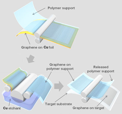
It turns out that graphene can be stabilized using standard roller technology used, for example, in the printing of newspapers and magazines. In this process, the hydrocarbon feed is deposited onto a smooth copper plate by reactive chemical deposition. An adhesive polymer coating is applied on top. Then the copper substrate is etched and the graphene is glued onto plastic sheets (PET) or another surface.
During the experiment, scientists from Korea and Japan received a rectangular sheet with a diagonal of 76 cm (pictured left).

In this way, you can even apply several layers of graphene on top of each other - and we get plastic with a graphene coating that can be cut into touchscreens of any size. According to experts, the commercial release of devices may begin in the coming years.
Touchscreens are just the beginning. The fact is that when graphene is rolled into a cylinder, a single-walled nanotube is obtained. If you find a good way to industrial production of nanotubes, then on graphene it is possible to create a new class of electronics with a base thickness of transistors up to 10 nm. Back in 2007, an experimental graphene transistor with a frequency of 30 GHz was created .
via Chemistry World
Graphene is a carbon film with a thickness of just 1 atom, in which the carbon atoms form a hexagonal lattice similar to a honeycomb. The graphene film was discovered in 2005 by a group of scientists from the University of Manchester (Novoselov, Game, Morozov, etc.). Five years after the discovery, it seems that the first acceptable method of its production was found.
It turns out that graphene can be stabilized using standard roller technology used, for example, in the printing of newspapers and magazines. In this process, the hydrocarbon feed is deposited onto a smooth copper plate by reactive chemical deposition. An adhesive polymer coating is applied on top. Then the copper substrate is etched and the graphene is glued onto plastic sheets (PET) or another surface.
During the experiment, scientists from Korea and Japan received a rectangular sheet with a diagonal of 76 cm (pictured left).
In this way, you can even apply several layers of graphene on top of each other - and we get plastic with a graphene coating that can be cut into touchscreens of any size. According to experts, the commercial release of devices may begin in the coming years.
Touchscreens are just the beginning. The fact is that when graphene is rolled into a cylinder, a single-walled nanotube is obtained. If you find a good way to industrial production of nanotubes, then on graphene it is possible to create a new class of electronics with a base thickness of transistors up to 10 nm. Back in 2007, an experimental graphene transistor with a frequency of 30 GHz was created .
via Chemistry World