Making a timer or first FPGA project
 I will start my first article with the fact that I will inform you: I am a beginner in the subject of the article, but I chose just such a topic. I will explain why. I have been reading habr for quite a long time and I have always been interested in topics of those who are currently studying what they are talking about. Such articles are always understandable, they always find their audience and always betray to the reader the interest and enthusiasm of the author, which is usually off scale for beginners in any field!
 So, recently I became interested in the topic of FPGAs, having encountered them while studying, I read a lot of docks and ordered a Starter Kit for experiments. Now, having received a training ground for experiments by mail and having completed the first experiment, I am ready to share it with habrausers. I hope it will be interesting.
First, let's go over the theory, what does the abbreviation FPGA mean in the topic of the article? You can always read the wiki yourself, so I’ll try to describe it myself. Who knows what FPGAs are, skip boldly.
FPGA (Programmable Logic Integrated Circuit) is one of the types of electronic devices used to implement various logic devices of various complexity, from binary counters, simple logic circuits (replacing standard integrated circuits - loose powder) to specialized processors and neurochips.
With the appointment sorted out, the question is - how? Inside the FPGA are some basic elements that are connected based on the configuration record. Possible basic elements, type and storage location of the configuration record depend on the type of FPGA and on a specific model. In modern FPGAs, two types are distinguished: CPLD and FPGA, we will give them in the paragraph.
CPLD (complex programmable logic device) - FPGA, the basic elements of which are macrocells and simple logic gates (AND (-HE) / OR (-HE)). Usually contains fewer base elements than FPGAs, but is faster. It also usually contains a non-volatile configuration memory directly on the chip, but has a limited number of configuration cycles.
FPGA (field-programmable gate array) - FPGAs, which usually have a whole bunch of types of base blocks, these are customizable logic elements (truth tables) and addition-multiplication blocks (Digital signal processing - DSP) and PLL (Phase -Locked Loop) for dividing and multiplying frequencies and some others depending on the model. Usually they have volatile internal memory and functionality for loading configurations from external non-volatile memory.
The definitions of these types of FPGAs and the differences between them can be found very different, both in books and on the Internet. Therefore, do not focus on this difference, manufacturers themselves classify the FPGAs they produce. If you didn’t remember the abbreviations or didn’t understand the meanings of some words - it’s not scary, the main thing is to have a general concept about FPGAs, I hope I have achieved this. And now to practice!
Let's start by discussing the tools. I will use the starter kit of the Altera Cyclone II FPGA Starter Board, this is a finished board on which the FPGA of the Cyclone II series is installed - EP2C20F484C7N, as well as various peripherals and interfaces. In this article, we use LEDs and seven-segment indicators. We will not use any special blocks of this FPGA series, so if you want you can use almost any other FPGA (FPGA and CPLD).

Those who are very interested can buy one of the developer’s kits or assemble the device themselves, which is quite difficult for a beginner, but quite a feasible task. The programmer circuits and the FPGA connection schemes themselves are easily googled, besides, those who previously worked on amateur AVR firmware can find the Altera Byte Blaster programmer that is suitable for themselves. In general, I provide you with a schematic implementation of a habrayuzer (At the end of the article is a diagram of my Starter Board). Those who want to try without money and see the result of work can use the simulator built into Quartus II (this article does not describe how to work with it).
From the software, we will use Quartus II, the free version of which you can find on the manufacturer's website (Altera), both in Windows and in Linux versions.
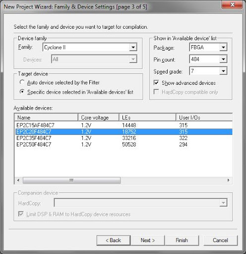
And now we have come close to practice! We launch our CAD Quartus II and create a project. The first steps of the wizard indicate the name of the project and its location, then skip the step of adding files (we still have time). We’ll finish the creation of the project at the stage of choosing a device, if we do it on a piece of iron - we know the name of the FPGA exactly, we select it. If we just make a project for FPGAs, we’ll choose something more powerful, for example, the third cyclone. I choose the FPGA that is installed in my starter kit.
Click Finish - the project is created. The project structure in Quartus is hierarchical, we need to select the top of the hierarchy (Top-Level Entity). We can use for design circuit files and files with a description of the logic on one of the HDL (Hardware description language - hardware description language). My opinion is to use the schematic file with the main logic blocks as the top of the hierarchy, and implement the blocks themselves in HDL. Opinions can be different, while choosing, reading a lot of holivarny topics, but so far focused on such a model, you can make your choice. As the HDL of the project language, I chose VHDL ((Very high speed integrated circuits) Hardware Description Language), you can use any other, for example Verilog or AHDL, it all depends on your preference.
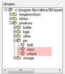
We create our first project file (File - New ..), select Block Diagram / Schematic File. Now let's draw the simplest circuit, add one Input, one Output and connect them (in a real FPGA, this circuit will transmit a signal from one leg to another). To do this, Double Click on an empty place in the diagram and in the Symbol dialog box that opens, select the necessary element.
We connect just like that, with a line. Let's give the pins the names (Double Click on the elements), input I will call CLOCK_27 [0], and output I will name LEDR [0]. The names were not chosen randomly - I then associate CLOCK_27 [0] with the input of the 27Mhz generator, and LEDR [0] with a zero red LED. We save the file, leaving a checkmark for adding to the project. Now set the resulting file to the top of the project hierarchy. For this, the Project Navigator window, in the Files tab, in the context menu of our file, select Set as Top-Level Entity. Hello, world is ready. We compile the project (Processing - Start Compilation), if we see Info: Quartus II Full Compilation was successful. - rejoice and believe that the first stage has been completed.
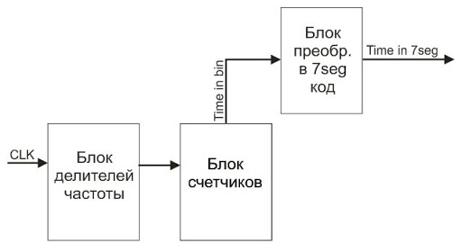
Now let's figure out our goals. Our device will start the countdown of minutes and hours when it is turned on. So we need four seven-segment indicators “HH: MM”. To count the time, we need a more or less accurate 1Hz signal. We will get it by dividing the frequency 27Mhz, then we will count it at 60 (seconds), then again at 60 (minutes), and then at 24 (hours). From the last two blocks, the binary number of minutes and hours will go to the Bin -> BCD (binary-coded decimal) -> 7seg decoder. Here, in general, is the whole device. Immediately make a reservation that the circuit will be asynchronous (Minutes start from seconds and hours from minutes), for simplicity and clarity.
So, let's create our first block - the frequency division block. Create a new file, as we already know, only the file type will be VHDL File. Insert the code into it:
library ieee;

use ieee.std_logic_1164.all;

use ieee.std_logic_unsigned.all;


entity Div_27Mhz_to_1Hz is

 port( clk:in std_logic; clk_out:out std_logic);

end Div_27Mhz_to_1Hz;


architecture div_behavior of Div_27Mhz_to_1Hz is

begin

 process(clk)

 variable cnt : integer range 0 to 27000000;

 begin

 if(clk'event and clk = '1')

 then


if(cnt >= 13500000)

 then

 clk_out <= '1';

 else

 clk_out <= '0';

 end if;


 if(cnt = 27000000)

 then

 cnt := 0;

 else

 cnt := cnt + 1;

 end if;


 end if;

 end process;

end div_behavior;
I’ll skip utility directives (you can see it in the directory, links at the end), I will pay attention only to the logic of work. First, we declare the entity, i.e. the block itself. We indicate its inputs and outputs, their types and names. Type std_logic in common means bit. Next, we describe the internal architecture of this unit. Architecture consists of parallel processes. Each process has its own sensitivity list, for example, the only process in the example above is sensitive to changes at the clk input. You can declare variables for the process, in our example it is an integer range 0 to 27000000 type variable. Next, the elementary logic is set in the body of the process: until half the period has passed - we shove logical zero into the output, as half passes - we shove one, and do not forget to count and reset the counter upon reaching 27000000.
We save the file with the code and create a symbol (File - Create / Update - Create Symbol Files For Current Files), this is necessary in order to insert this block into our main scheme. You can find your characters in the Project folder in the character insert dialog. Now go over the remaining blocks in less detail. This is a counting block from zero to 59, which we use to count minutes and seconds. Of the new products here, the output type is std_logic_vector (5 downto 0), which determines the group of bits (bit vector), as well as the function CONV_STD_LOGIC_VECTOR (cnt, 6), which converts the variable into a bit vector of the specified length. Higher hours counter. Nothing new.
library ieee;

use ieee.std_logic_1164.all;

use ieee.std_logic_unsigned.all;


-- For CONV_STD_LOGIC_VECTOR:

use ieee.std_logic_arith.all;


entity cnt_0_to_59 is

 port( clk:in std_logic; c59:out std_logic; vector:out std_logic_vector(5 downto 0));

end cnt_0_to_59;


architecture cnt_behavior of cnt_0_to_59 is

begin

 process(clk)

 variable cnt : integer range 0 to 59;

 begin

 if(clk'event and clk = '1')

 then

 if(cnt = 59)

 then

 cnt := 0;

 c59 <= '1';

 vector <= CONV_STD_LOGIC_VECTOR(cnt, 6);

 else

 cnt := cnt + 1;

 c59 <= '0';

 vector <= CONV_STD_LOGIC_VECTOR(cnt, 6);

 end if;

 end if;

 end process;

end cnt_behavior;
library ieee;

use ieee.std_logic_1164.all;

use ieee.std_logic_unsigned.all;


-- For CONV_STD_LOGIC_VECTOR:

use ieee.std_logic_arith.all;


entity cnt_0_to_23 is

 port( clk:in std_logic; vector:out std_logic_vector(4 downto 0));

end cnt_0_to_23;


architecture cnt_behavior of cnt_0_to_23 is

begin

 process(clk)

 variable cnt : integer range 0 to 23;

 begin

 if(clk'event and clk = '1')

 then

 if(cnt = 23)

 then

 cnt := 0;

 vector <= CONV_STD_LOGIC_VECTOR(cnt, 5);

 else

 cnt := cnt + 1;

 vector <= CONV_STD_LOGIC_VECTOR(cnt, 5);

 end if;

 end if;

 end process;

end cnt_behavior;
library ieee;
use ieee.std_logic_1164.all;
use ieee.std_logic_unsigned.all;
-- For CONV_STD_LOGIC_VECTOR:
use ieee.std_logic_arith.all;
entity bin2bcd_5bit is
port( bin:in std_logic_vector(4 downto 0);
bcd1:out std_logic_vector(3 downto 0);
bcd10:out std_logic_vector(3 downto 0)
);
end bin2bcd_5bit;
architecture converter_behavior of bin2bcd_5bit is
begin
process(bin)
variable i : integer range 0 to 23;
variable i1 : integer range 0 to 9;
begin
i := conv_integer(bin);
i1 := i / 10;
bcd10 <= CONV_STD_LOGIC_VECTOR(i1, 4);
i1 := i rem 10;
bcd1 <= CONV_STD_LOGIC_VECTOR(i1, 4);
end process;
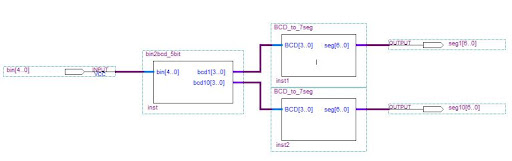
end converter_behavior;The Binary to BCD Converter essentially just splits one binary number into two, each representing a decimal place. Of the new products - the rem operator, the remainder of the division. The converter for six bits is written in the same way, I will not give it. A converter of one bit into a seven-segment code implemented by a simple truth table. The seven-segment code itself is a bit representation of the burning segments on the indicator in the abcdefg order, in my case also inverse.
library ieee;

use ieee.std_logic_1164.all;

use ieee.std_logic_unsigned.all;


entity BCD_to_7seg is

 port(

 BCD:in std_logic_vector(3 downto 0);

 seg:out std_logic_vector(6 downto 0)

 );


end BCD_to_7seg;


architecture conv_behavior of BCD_to_7seg is

begin

 process(BCD)

 begin

 if BCD = "0000" then seg <= "0000001";--0

 elsif BCD = "0001" then seg <= "1001111";--1

 elsif BCD = "0010" then seg <= "0010010";--2

 elsif BCD = "0011" then seg <= "0000110";--3

 elsif BCD = "0100" then seg <= "1001100";--4

 elsif BCD = "0101" then seg <= "0100100";--5

 elsif BCD = "0110" then seg <= "0100000";--6

 elsif BCD = "0111" then seg <= "0001111";--7

 elsif BCD = "1000" then seg <= "0000000";--8

 elsif BCD = "1001" then seg <= "0000100";--9

 else seg <= "1001001";--err

 end if;

 end process;

end conv_behavior;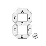
So we realized all the blocks, it remains to connect them together. I will give the Main scheme and decoding of the bin2seg symbol, which is also implemented as a scheme to save space.
Main circuit:
(click-click)
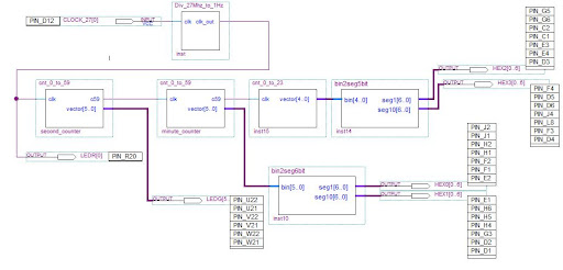
(As you can see in the diagram, I displayed the count of seconds on the green LEDs, again for clarity)
bin2seg:
(click-click)
The project is ready, you can compile and test. I wanted to talk about modeling the operation of the circuit in a quartus, but something happened so much, there will be interest - I will write in the next article. Now the last step is to associate our virtual inputs / outputs with real FPGA legs.
Association can be carried out after compilation in the Assignments - Pins menu. In the window that appears, you will see the pin layout on the chip and below it a list of project pins. By changing the Location field, we map the internal inputs to the real legs. In my case, I look at the pin names according to the layout of my board, and in the case of your development, you will know the pin names. The last step is the firmware, it is carried out from the Tools - Programmer menu, by the start button (the programmer must be connected and the drivers are installed).
Well, sort of everything. In conclusion, I want to say that in the presence of public interest in this topic I will certainly write more articles. For example, how to finish this project to normal hours with a setting and an alarm clock or something new, I already have plans :)
Promised links:
www.altera.com - all kinds of documentation and product advertising
www.bsuir.by/vhdl/reference - VHDL directory
altera.ru - our Altera representative, I ordered a starter kit there
+ I used a book by J.R. Armstrong Modeling digital systems in VHDL.
For those who undertake to assemble myself, I attach the circuit of my board. ( kach )
And also a bonus - a timer project ( kach-kach )