UDB. What is it? Part 7. Timing and reset control module
- Transfer
The next chapter from the official Cypress documentation about managing timing and reset. As mentioned in the first article of this series, this module provides timing selection and resolution, as well as reset selection within UDB. More details - under the cut.
General content of the cycle “UDB. What is this? ”
Part 1. Introduction. Pld.
Part 2. Datapath.
Part 3. Datapath FIFO.
Part 4. Datapath ALU.
Part 5. Datapath. Useful little things.
Part 6. Management and status module.
Part 7. Timing and reset control module. (Current article)
Part 8. Addressing UDB
21.3.4 Reset and Clock Control Module
The main function of this module is to select clocks from the available global clocks or bus clock for each PLD, Datapath, and control and status module. The module also supports dynamic and soft dumps of UDB blocks. As shown in Figure 21-38, there are four clock control units and one reset control unit. Four inputs (RC_IN [3: 0]) are available for forwarding from the global trace matrix. Each clock control unit can select a source for the clock enable input from these trace inputs, and there is also a multiplexer that allows you to select one of the trace inputs for use as an external clock source. As you can see in the figure, the choice of an external clock source can be synchronized. For each UDB component, there are 10 clocks to choose from: 8 global digital clocks, a bus clock, and a selected external clock (ext clk). Any of the traced input signals (rc_in) can be used either as a level-sensitive activator or as an edge-sensitive activator. The reset function of this block provides a traced reset of the PLD blocks and the SC counter, as well as the ability to programmatically reset each block to support reconfiguration.
The bus clock applied to the clock and reset control module is different from the system bus clock. This signal is called "bus_clk_app" and is locked in the same way as other digital clock signals. The clock signal of the system bus is used only for input-output operations and is automatically unlocked for each access. The Datapath Clock Generator generates three clocks: one for Datapath and one signal for each FIFO.
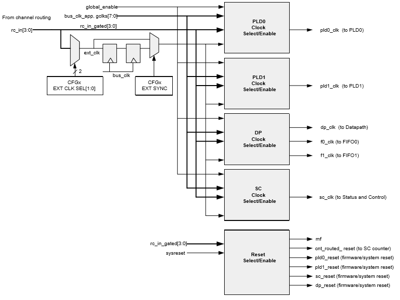
Figure 21-38. Clock and reset control module.
21.3.4.1 Clock control
Figure 21-39 shows an example of a clock selection and resolution scheme. Each UDB has four such schemes: one for each PLD block, one for Datapath, and one for the control and status block. The main components of this circuit are the global clock selector multiplexer, the clock inverter, the clock enable signal multiplexer, the clock enable signal inverter and the differential detection logic.
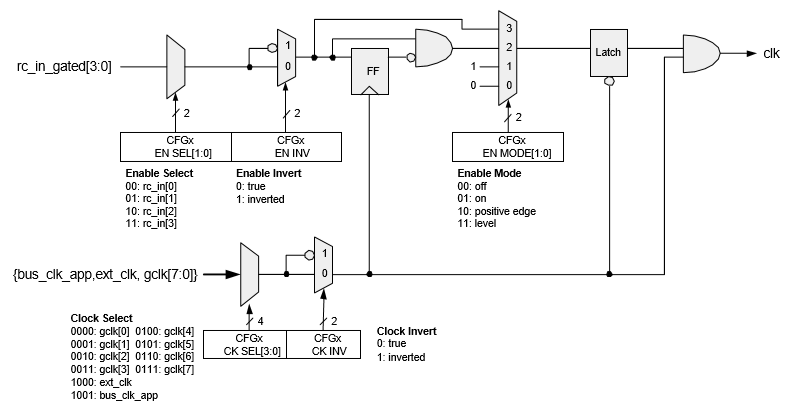
Figure 21-39. Manage selection / activation of timing.
Clock Selection
There are eight global digital clocks forwarded to all UDBs. Any of them can be selected. Global digital clocks are outputs of frequency dividers selected by the user. See “Timing System” on page 109 of the original. Another option is the bus clock, which has the highest frequency in the system. This signal is called "bus_clk_app" and is traced separately from the system bus clock. In addition, to support functions with a direct clock signal (for example, SPI), an external trace line can be selected as an input clock signal. Since application functions are tied to arbitrary boundaries within the UDB, selecting an individual clock signal for each UDB subcomponent contributes to precise granularity in programming.
Clock Inversion
The selected clock signal can be inverted. This will limit the maximum frequency of work due to the existence of sections with a half-cycle cycle. Simultaneous bus recording and internal recordings (for example, program recording a new counter value during its operation) are not supported when the internal clock is inverted and has the same frequency as the bus clock. This restriction affects A0, A1, D0, D1, as well as the control register in counter mode.
Clock Enable Selection The
clock enable signal can be forwarded to any synchronous signal and selected at any of the four inputs of the trace matrix available to this block.
Clock Enable Inversion
The clock enable signal can be inverted. Due to this, this signal can be generated in any polarity.
Clock Enable Modes
By default, the clock enable mode is set to OFF. After setting the operation of the target unit, the software can set one of the operating modes described below using the CFGxEN MODE [1: 0] register, shown in Figure 21-39.
Table 21-23. Timing Resolution Modes.
| Timing Resolution Modes | Description |
|---|---|
| Off | Clocking is disabled. |
| ON | Clocking is included. The selected global clock runs freely. |
| Positive edge | A skipped clock pulse is generated for each positive edge at the resolution input. The maximum allowable frequency at the resolution input is half the clock frequency. |
| Level | Clock pulses are generated while the clock enable input is at a high level ('1'). |
Using Clock Permissions
There are two common scenarios for using clock permissions.
Software Enable (Firmware Enable) : It is assumed that most functions require software clock enable to start and stop the function. Since the boundary of a function bound to a UDB array is conditional, a function can span several UDBs and / or parts of a UDB. Therefore, a way is needed to include each function atomically. This is usually implemented using a bit in the control register, forwarded to one or more clock enable inputs. This scenario also supports the case where applications need to run multiple unrelated blocks at the same time.
Emulated Local Clock Generation: This feature allows UDBs to generate local clocks and distribute them to other UDBs in the array using the synchronization clock activation implementation template, rather than directly clocking each UDB separately. Using the Positive Edge function to enable resolution removes restrictions on the duty cycle of the resolution signal.
Special
FIFO Timing FIFO Datapath blocks have timing features. By default, FIFO clocking has the same configuration as Datapath clocking. However, FIFO blocks have special control bits that change the clock configuration:
- each FIFO clock can be inverted relative to the polarity of the selected Datapath clock;
- when FIFO FAST mode is selected, the bus clock replaces the Datapath clock option, which typically uses FIFO.
21.3.4.2 Reset management
There are two modes of reset management: inherited and standard. The mode is set using the ALT RES bit in each configuration register of the UDB CFG31. By default, the bit value is 0 (legacy mode); it is recommended to assign it a value of 1 (standard mode). Standard mode has a greater degree of granularity - individual blocks within the UDB can use traceable flushes. For information on legacy mode, contact Cypress.
PLD Reset Control
Figure 21-40 shows a PLD reset system.

Figure 21-40. Reset Structure PLD.
Datapath Reset Control
Figure 21-41 shows the Datapath reset system. Traced flush applies to all Datapath registers and states except data registers D0 and D1. Data registers are persistent registers. The content of the FIFO is not defined after the reset, as it is located in RAM.

Figure 21-41. Datapath reset structure.
Status and Control Reset Control
Figure 21-42 shows the control and status reset system. The control / counter and status registers have a common trace reset, however they are enabled separately. The mask / period and auxiliary control registers are save registers.
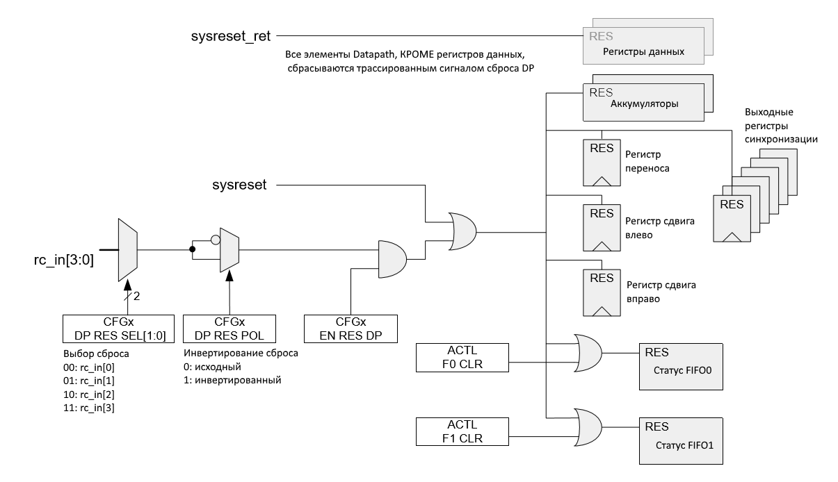
Figure 21-42. Reset management and status management.
21.3.4.3 Power On UDB Initialization (POR)
Register and State Initialization
Table 21-24. Initialization of UDB states when enabled
| State item | Decoding a status item | Power On Status |
|---|---|---|
| CFG 0 - 31 | Configuration latches | 0 |
| Ax, Dx, CTL, ACTL, MSK | Batteries, data registers, auxiliary control register, mask register | 0 |
| ST, MC | Status and macrocell registers (read-only) | 0 |
| DP CFG RAM & Fx (FIFO) | Datapath configuration RAM and FIFO RAM | Unknown |
| PLD RAM | Ram configuration pld | Unknown |
Tracing Initialization
When enabled, the state of trace inputs and outputs has the following features:
- all UDB outputs that direct data to the trace matrix are held at '0';
- all drivers coming out of the trace and entering the UDB inputs are initially zeroed.
This initialization avoids conflicting states during tracing, and the initial configuration occurs in a sequence in which order does not matter.
The ending follows. We are preparing the