The union of Arduino and the classic processor
- Transfer
- Tutorial

Retrocomputers come in varying degrees of finicky. Some are content with emulation. Others prefer FPGAs, because then it turns out not emulation, but recreation. Finally, serve the third processor.
But the processor needs so much to work! Again, the dilemma: take real chips of the same years, or put everything in the FPGA, leaving the processor outside? However, why is FPGA necessary? Long live the union of the Arduino and the classic processor!
Give your Arduino a “second brain” and make it smarter.
A true eight-bit microprocessor runs programs, while an Arduino emulates ROM, RAM, and simple peripherals.
Design virtual peripherals in the Arduino IDE, and run the assembler code on the microprocessor. No need to assemble complex circuits and flash parallel ROMs.
Supported microprocessors: 6502, 6809 and Z80 (КР1858ВМ1), others are on the way.
A shield with a microprocessor does not interfere with connecting other shields: with LCDs, memory cards, etc.
In addition to self-programming in assembler, you can try to run some classic code on the microprocessor.
True, the microprocessor will operate at a very low frequency - about 95 kHz, its exact value depends on the optimization of the peripheral emulation code.
The distribution of address space is set programmatically in a sketch. The microprocessor can be allocated from 4 to 6 kB of 8 kB RAM available on the Arduino Mega. ROM can allocate more than 200 kB of the available 256.
Using the Arduino Mega serial port, you can emulate UART.
Circuits, board drawings, Gerber files are available under CC-BY-SA 4.0 here . At the same time, there is a requirement to attach the README.md file, because it contains the following warning:
Do not connect the shield until the peripheral emulation sketch is uploaded! Otherwise, shorting the output lines of the microprocessor is possible.Yes, and in the sketch itself, something needs to be redone carefully for the same reason.
Device diagram for 6502:

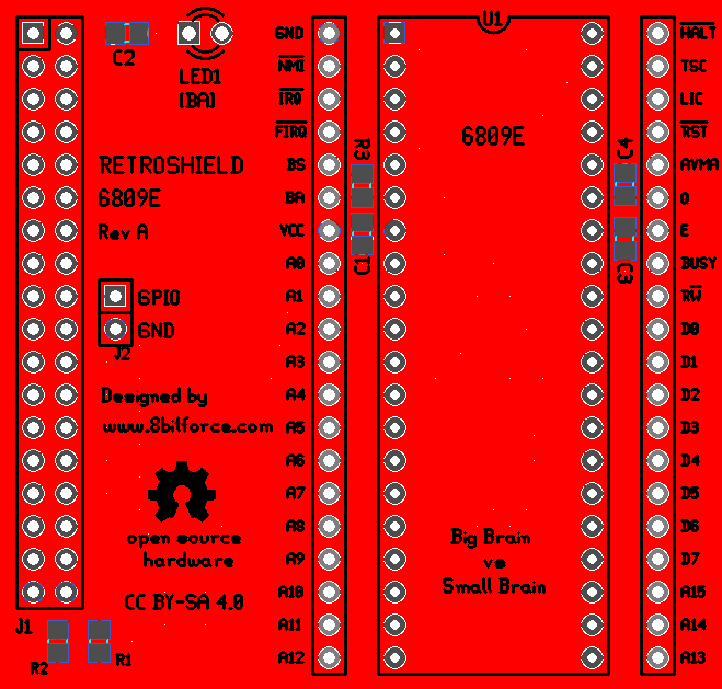
Device diagram for 6809:

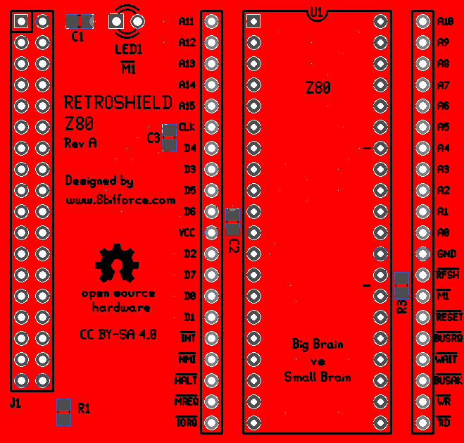
Device diagram for Z80:

You can already start:
On a device with 6502 - Apple I, Woz Monitor + ROM with BASIC
On a device with 6809 - An analog of a home-made computer Simon6809 of the same developer, a training monitor with assembler and a disassembler
On a device with Z80 - so far only an echo test of the serial port , allowing you to check the performance of the virtual 8251 (KR580VV51A).
Firmware for emulating peripherals - under the MIT license.
Brief descriptions of the principle of operation:
To a device on 6502
To a device on 6809
To the device on the Z80 - in preparation.
The developer is trying to sell devices, but with delivery only in the United States. There is no particular reason to buy, because the scheme is very simple, you can repeat it on a piece of the breadboard in an hour.
It is planned to develop similar boards on RCA1802, 68008, 8085 (КР1821ВМ85А), 8088 (КР1810ВМ88). About K1801BM1 is not said, but you can throw such an idea to the author.
Files:
To the device on 6502: assembly instructions , silk screen printing , diagram
To the device on 6809: assembly instructions , silk screen printing , diagram
To the device on Z80: assembly instructions , silk screen, circuit
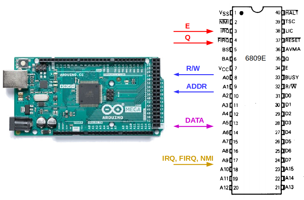
Consider the interaction of an Arduino and a 6502 device. Arduino periodically changes the level at the microprocessor input, designed to supply clock pulses, from zero to one and back. At each cycle, it checks what is happening on the control lines and the address bus, and, depending on the situation, reads information from the data bus or sends it there. Arduino can also control IRQ and NMI lines, causing interruptions. The figure shows the types of data and the directions of their transmission: The

correspondence of the Arduino ports and the microprocessor outputs is configured in the sketch:
/* Digital Pin Assignments */
#define DATA_OUT    PORTL
#define DATA_IN     PINL
#define ADDR_H      PINC
#define ADDR_L      PINA
#define ADDR        ((unsigned int) (ADDR_H << 8 | ADDR_L))
#define uP_RESET_N  38
#define uP_RW_N     40
#define uP_RDY      39
#define uP_SO_N     41
#define uP_IRQ_N    50
#define uP_NMI_N    51
#define uP_E        52
#define uP_GPIO     53
We divide each measure into the following events:
CLK changes state from one to zero (fall)
CLK is in zero state
CLK changes state from one to zero (rise)
CLK is in state one
CLK again changes state from one to zero ...
What happens in moments state transitions?
6502 receives clock pulses at input CLK0, buffers them and sends them to two outputs: CLK1 and CLK2. Although all events in the microprocessor are tied to CLK1, we assume that the delay is not large, and they are tied to CLK0 - the line along which the microprocessor receives clock pulses from Arduino. And call the signal just CLK.

1. CLK changes state from one to zero.
2. The microprocessor outputs a new address to the address bus, and a switch signal between reading and writing to the R / W output. But he is not ready for data exchange yet.
3. CLK goes into unit state, and this means that the exchange of data has begun. If this is a read operation, the microprocessor transfers the data bus outputs to the input state and receives data, and if the write operation, it transfers them to the output state and sends data. And the R / W signal switches the external device to the write or read mode, the opposite of the corresponding state of the microprocessor.
4. CLK goes to zero. Now neither the microprocessor nor the input-output devices output anything to the data bus. The microprocessor can set the data bus line and the R / W pin to a new state.
A simple explanation, understandable to the child. Who never thinks about these "behind the scenes intrigues", if he will only program microcontrollers. Even in assembler.
If you need to connect your peripheral device, it must have time to prepare the data before the unit (preparation time) appears on the CLK line, and while the unit is there, do not change it. If the peripheral device does not have time to prepare the data while CLK is zero, or changes it when the unit is there, you will wonder for a long time why your code does not work. Since the clock frequency of the microprocessor is ten to fifteen times lower than the nominal frequency, it is easy to comply with this requirement. But it is necessary.
So, you need to “teach” Arduino to generate clock pulses, continuously checking what happens on the address and R / W lines, and interacting with the data bus accordingly. To do this, the sketch uses the timer1 timer interrupt, which generates pulses with a frequency of 95 kHz. Arduino works much faster than the microprocessor, and therefore, between its clocks, it manages to read and prepare everything. It is important to ensure that after modifying the sketch this condition continues to be met.
Here is an excerpt from the sketch, which shows how the CLK goes from zero to one, and what happens next:
////////////////////////////////////////////////////////////////////
// Processor Control Loop
////////////////////////////////////////////////////////////////////
// This is where the action is.
// it reads processor control signals and acts accordingly.
//
ISR(TIMER1_COMPA_vect)
{
  // Drive CLK high
  CLK_E_HIGH;
  // Let's capture the ADDR bus
  uP_ADDR = ADDR;
  if (STATE_RW_N)
  //////////////////////////////////////////////////////////////////
  // HIGH = READ transaction
  {
    // uP wants to read so Arduino to drive databus to uP:
    DATA_DIR = DIR_OUT;
    // Check what device uP_ADDR corresponds to:
    // ROM?
    if ( (ROM_START <= uP_ADDR) && (uP_ADDR <= ROM_END) )
      DATA_OUT = pgm_read_byte_near(rom_bin + (uP_ADDR - ROM_START));
    else
    if ( (BASIC_START <= uP_ADDR) && (uP_ADDR <= BASIC_END) )
      DATA_OUT = pgm_read_byte_near(basic_bin + (uP_ADDR - BASIC_START));
    else
    // RAM?
    if ( (uP_ADDR <= RAM_END) && (RAM_START <= uP_ADDR) )
      DATA_OUT = RAM[uP_ADDR - RAM_START];
    else
    // 6821?
    if ( KBD <=uP_ADDR && uP_ADDR <= DSPCR )
    {
      // KBD?
      if (uP_ADDR == KBD)
      {
        ... // handle KBD register
      }
      else
      // KBDCR?
      if (uP_ADDR == KBDCR)
      {
        ... // handle KBDCR register
      }
      else
      // DSP?
      if (uP_ADDR == DSP)
      {
        ... // handle DSP register
      }
      else
      // DSPCR?
      if (uP_ADDR == DSPCR)
      {
        ... // handle DSPCR register
      }
    }
  }
  else
  //////////////////////////////////////////////////////////////////
  // R/W = LOW = WRITE
  {
    // RAM?
    if ( (uP_ADDR <= RAM_END) && (RAM_START <= uP_ADDR) )
      RAM[uP_ADDR - RAM_START] = DATA_IN;
    else
    // 6821?
    if ( KBD <=uP_ADDR && uP_ADDR <= DSPCR )
    {
      // KBD?
      if (uP_ADDR == KBD)
      {
        ... // handle KBD register
      }
      else
      // KBDCR?
      if (uP_ADDR == KBDCR)
      {
        ... // handle KBDCR register
      }
      else
      // DSP?
      if (uP_ADDR == DSP)
      {
        ... // handle DSP register
      }
      else
      // DSPCR?
      if (uP_ADDR == DSPCR)
      {
        ... // handle DSPCR register
      }
    }
  }
  ////////////////////////////////////////////////////////////////
  // We are done with this cycle.
  // one full cycle complete
  clock_cycle_count ++;
  // start next cycle
  CLK_E_LOW;
  // If Arduino was driving the bus, no need anymore.
  // natural delay for DATA Hold time after CLK goes low (t_HR)
  DATA_DIR = DIR_IN;
}
Address space allocation can be done as you like, in an unmodified sketch it is the same as in Apple 1 with 256 bytes of ROM, 8 kilobytes of ROM for BASIC, 4 kilobytes of RAM and 6821 input-output device.
// MEMORY LAYOUT
// 4K MEMORY
#define RAM_START   0x0000
#define RAM_END     0x0FFF
byte    RAM[RAM_END-RAM_START+1];
// ROMs (Monitor + Basic)
#define ROM_START   0xFF00
#define ROM_END     0xFFFF
#define BASIC_START 0xE000
#define BASIC_END   0xEFFF
////////////////////////////////////////////////////////////////////
// Woz Monitor Code
////////////////////////////////////////////////////////////////////
//
PROGMEM const unsigned char rom_bin[] = {
    0xd8, 0x58, 0xa0, 0x7f, 0x8c, 0x12, 0xd0, 0xa9, 0xa7, 0x8d, 0x11, 0xd0,
    ...
    0x00, 0xff, 0x00, 0x00
};
// BASIC ROM starts at E000
PROGMEM const unsigned char basic_bin[] = {
    0x4C, 0xB0, 0xE2, 0xAD, 0x11, 0xD0, 0x10, 0xFB,
    ...
    0xE0, 0x80, 0xD0, 0x01, 0x88, 0x4C, 0x0C, 0xE0
};
RAM is emulated by byte RAM array [RAM_END-RAM_START + 1]. Two PROGMEM keywords are needed so that the contents of emulated ROMs are stored in the flash memory of the microcontroller.
6821 is emulated enough that virtual keyboard and display work through the “terminal”. Woz Monitor and BASIC work, which is what the author sought.
To emulate any peripheral device, you need to carefully read its datasheet and find out what registers it has and what they are for. The convenience of emulation lies in the flexibility with which you can make software analogues of the periphery.
I / O devices are located in the address space of the microprocessor; they are accessed in the same way as memory cells. To use the "iron" peripherals, such as an LCD display, a memory card, sound output, you need to allocate a place in the address space.
Links:
www.6502.org
www.callapple.org/soft/ap1/emul.html
skilldrick.github.io/easy6502
searle.hostei.com/grant/6502/Simple6502.html
wilsonminesco.com/6502primer
SB-Assembler: www .sbprojects.net / sbasm
We turn to 6809, it contains:
Two eight-bit accumulators A and B, which can be combined into one six
-bit accumulator Two 16-bit stack indexes
Addressing relative to the instruction counter
Automatic addition or subtraction of the number 1 or 2
Multiplication of two eight-digit unsigned numbers
16-bit arithmetic
Transfer and data exchange between all registers
Writing and reading all registers and any combination of them
The microprocessor 6809E (external) needs an external clock generator, for 6809 it has an internal one. For Hitachi, they are called, respectively, 6309E and 6309, they differ from the usual ones in that they operate in 32-bit form inside the operation, but it is possible to switch to compatibility mode with the classic version.
Actually, the whole RetroShield project started because the author wanted to upgrade his home-made computer Simon6809 and name the result Simon6809 Turbo. But it turned out that standard logic chips for everything that he wanted to implement there would require a lot. Therefore, the author formulated the idea of RetroShield for the first time in relation to 6809, and only then thought: “what if the same with other processors do the same?”.
The device, of course, uses the 6809E, which requires an external clock, so that it can synchronize its work from the outside. The E and Q lines for both processors are named the same, only 6809 have outputs, and 6809E have inputs.
Arduino interacts with 6809 in the same way as with 6502, but it has two clock inputs: E and Q, and three interrupt inputs: IRQ, FIRQ and NMI.
This time, the correspondence between the Arduino ports and the microprocessor pins is configured as follows:
/* Digital Pin Assignments */
#define DATA_OUT PORTL
#define DATA_IN  PINL
#define ADDR_H   PINC
#define ADDR_L   PINA
#define ADDR     ((unsigned int) (ADDR_H << 8 | ADDR_L))
#define uP_RESET_N  38
#define uP_E        52
#define uP_Q        53
#define uP_RW_N     40
#define uP_FIRQ_N   41
#define uP_IRQ_N    50
#define uP_NMI_N    51
#define uP_GPIO     39
As can be seen from the graphs, the signal Q is shifted relative to E by a quarter of the period:
We will hardly pay attention to Q, since all events are tied to E. And everything happens like this:
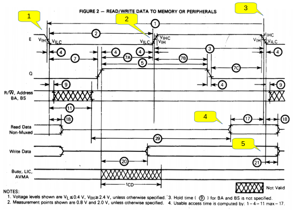
- E switches to zero. The processor sets a new address on the address bus and changes the state of the R / W line.
- E switches to one, the processor becomes ready for data exchange.
- It doesn’t matter what happens to the data bus as long as E is one, the main thing is that the required data is there when E goes back to zero.
- When reading data, the I / O device must supply the required data to the data bus before the line E passes from one to zero (the minimum delay is shown by the number 17 in the circle).
- When recording, the I / O device must fix the data in some register in the form in which it was at the time E went from one to zero. The processor will provide this data on the bus even earlier - at the moment of transition of Q to one (the number 20 in the circle).
- After the transition of E to zero, everything repeats.
Everything said above about 6502 about the need to generate all the signals by the peripheral device (including virtual one) in time also applies to 6809.
Generation of E and Q signals, as in the case of 6502, with the only difference that there are two signals, and switch them necessary in accordance with the schedules. And just like that, a subroutine called upon interruption performs data input or output at the required moments.
The address space in the unmodified sketch is distributed in the same way as in the home-made Simon6809 computer :
// MEMORY
#define RAM_START   0x0000
#define RAM_END     0x0FFF
#define ROM_START   0xE000
#define ROM_END     0xFFFF
byte RAM[RAM_END-RAM_START+1];
////////////////////////////////////////////////////////////////////
// Monitor Code
////////////////////////////////////////////////////////////////////
// static const unsigned char
PROGMEM const unsigned char simon09_bin[] = {
    0x1a, 0xff, 0x4f, 0x1f, 0x8b, 0x0f, 0x36, 0x7f, 0x01, 0xa5, 0x10, 0xce,
    ...
    0x00, 0x09, 0x00, 0x0c, 0x00, 0x0f, 0xe0, 0x00
};
RAM and ROM are stored in arrays in the same way as in the 6502 variant, with the only difference being that there is only one array with ROM data.
I / O devices are also allocated portions of the address space, and they can be either virtual or real. Since Simon6809 is a modern machine based on a vintage elemental base, it exchanges data via FTDI from the PC on which the “terminal” is running. Here it is emulated.
Links:
A lot of information on 6809 on the Arto Page
Wikipedia article on 6809
SWTPc 6809 systems
Wikipedia article on the FLEX operating system