Sources of energy release on an IC chip
All modern microelectronics is based on semiconductors. Zones of different conductivity are created on the crystal, which are combined into some logic. Crystals work by consuming electrical energy and converting it into heat. This article describes the main processes that consume energy during the operation of ICs.
The source of heat generation on the IC chip is three main processes: dynamic power, short circuit, and leakage currents . A review of these processes will be carried out on the example of n-MOS technology (although everything described will be true for p-MOS)
1. Leakage currents in the IC- This process attracts the closest attention today. For a technical process of 250 μm or more, leakage currents did not significantly affect the overall energy consumption of ICs, however, with the development of technologies and the transition to a finer manufacturing process for creating MOS structures, quantum-mechanical effects began to have a significant effect on leakage currents. This process manifests itself most of all in the IC when it is in standby mode, as other leakage channels become insignificant. To create low-power ICs, you need to consider in more detail where and how leakage processes occur.
1.1 Reverse gate current: The effect in the region under the gate, which occurs under the condition VGS ≈ VT and VDS> 0 (for n-mops). In this area, when the transistor is closed, there is no voltage to form a conducting channel, however, some electrons can receive enough energy to move from source to drain. This current is called gate. The approximate values of this current can be calculated by the formula:
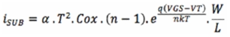
where:
isub = gate current;
a = constant dependent on the process or technology;
T = temperature in Kelvin;
Cox = capacity of the oxide layer;
n = another constant depending on the process or technology;
VGS = source gate voltage;
k = Boltzmann constant;
VT = voltage transition MOS cells from one state to another;
W = channel width;
L = channel length;
q = electron charge.
As can be seen from the formula, the gate current increases with decreasing channel length, and with decreasing transistor voltage VT and increasing temperature increases exponentially. With a decrease in the manufacturing process for manufacturing CMOS structures, the channel length and threshold voltage VT inevitably decrease for better logic performance (a high value of VT slows down the switching speed of the transistor). Thus, the gate current increases with decreasing process technology and becomes essential for technologies in the nanometer range. When the transistor is switched to a mode of reduced supply voltage, a favorable environment sets in for the appearance of a significant gate gate leakage current, since the switching voltage of the transistor decreases.

Fig. 1. Different currents in the structure of an n-MOS transistor.
2. Depletion of the potential barrier by runoff. When a voltage is established at the drain, it generates a depletion zone around itself with some potential. With a large distance between the electrodes of the MOS transistor, the influence of the drain field on the source remains negligible and, accordingly, no changes are made to the voltage between the source and the channel. However, with a decrease in the process technology, the distance between the drain and the source is reduced. As a result, the source is affected by the depletion zone and drain voltage. Its potential barrier decreases, which leads to the fact that the electron flux from source to drain increases, and the voltage at the source decreases.
1.3 Breakdown. This effect is an extreme state of depletion of the potential barrier, when the voltage at the drain reaches a certain value, after which the electron flux grows like an avalanche. This current is directly dependent on VDS (voltage between drain and source). This is one of the factors that determines the maximum possible voltage on a transistor. With a decrease in the size of the MOSFET, the distance between the drain and the source decreases, and the same VDS voltage at the smaller transistor will create a larger electric field. This field can cause breakdown, therefore, with a decrease in the process technology, it becomes necessary to reduce the operating voltage at the transistor.
1.4 Gate initiated current. Imagine that the drain is connected to the supply voltage, and the gate to ground or to negative power. Such a situation will lead to the appearance of a dense electric field in the drain region under the gate, the formation of a depletion region there and the appearance of interband tunneling. Since the substrate is connected to the ground, minority carriers collected in this depleted drain region under the influence of the field begin to penetrate the substrate. This current is called the gate initiated. This current is highly dependent on the voltage at the drain and on the thickness of the gate insulator.
1.5 Tunnel current through the gate. As the process decreases, the thickness of the oxide insulator under the gate also decreases. Currently, this thickness is 1 - 2 nm. A highly doped channel and an ultrathin insulation layer cause a very dense electric field, measured in MV / cm, to appear in the insulation region. With this field, charge carriers can already pass through the oxide insulator, creating a current through the gate. The greater the applied voltage, the more current will flow through the insulator. This current not only leaves through the gate, but can also greatly weaken the operating current through the drain. This may cause the transistor to malfunction. A polycrystalline silicon gate is used to combat this leakage current in transistors.
1.6 Reverse bias current. Between the diffusion zone n + and the substrate, a parasitic diode effect appears. This effect leads to the fact that minority charge carriers begin to penetrate from the drain onto the substrate. Electron hole pairs appearing in the depletion region also contribute to leakage to the substrate. This current is directly related to the density of the dopant and increases with increasing density.
2. Short circuit- another process that takes energy in the IC. When a change in the logic state appears at the input of the circuit, the circuit changes its output state. As a result of this process, MOS can transition from the “off” state to the “on” state, and in the opposite direction. Since transients do not occur instantly, a situation may arise in which a pair of n-MOS and p-MOS change their state and at some point none of them is in the “off” state. During this period of time, a short circuit occurs. This current is not caused by the charge of any electric capacitance inside the crystal, therefore this short circuit leads to a net loss of energy.

Fig. 2. Short circuit condition in the MOS inverter.
Imagine a situation where at the input of inverter A the state changes from low to high. The n-MOS transistor (lower) starts to open when a certain voltage Vn-MOS at input A is reached, and at this time the upper p-MOS transistor is still open. It will start to close when the input voltage reaches a certain high Vp-mop value. There is a situation when both transistors are open and a short circuit occurs. When any transistor closes, the circuit closes. The same process occurs when the input signal changes from high to low. The fault current becomes significant if the front / fall of the input signal continues for a long time and if output Z is connected to a low resistance. To combat such an effect, the front and decay of the wave are made faster and increase resistance,
3. Dynamic power is the process of power dissipation by switching the states of logic cells and, accordingly, the state of their inputs and outputs. For this reason, the process is also called switching energy. When a cell changes its logical state from high to low or vice versa, many internal capacities (at intersections, conductor connections, etc.) are charged and discharged, respectively.
This process was the most significant of all energy consumption processes up to technologies in 250 microns. With a decrease in the process technology, stray capacitances decreased, and the energy for switching the state also. However, there are ways to reduce dynamic power in order to reduce the overall power consumption of the IC.

Fig. 3. Switching current with MOS circuit.
Consider an elementary diagram of MOS elements. If all stray capacitances in the MOS cell are represented as a single capacitor C, then at the moment the output is switched from VDD to GRD, an energy consumption equal to CVDD2 will occur. Half of the energy will accumulate in the tank, the other half is lost. Similarly, when the output switches to VDD, the same process occurs. The switching energy is directly dependent on the VDD voltage and switching frequency. As a result, a way to reduce dynamic power is to reduce the supply voltage. However, this decrease leads to the fact that the cells become slower and the frequency decreases behind them. Consequently, more time will be spent on operations.
General dynamic power formula:
P = f * C * V * V
where f is the frequency, C is the capacitance, V is the voltage. Note that the dynamic power does not depend on the time of the front or the decay of the wave at the inputs and outputs.
Another component of dynamic power is energy losses due to multiple “unnecessary” switching, which can occur in the circuit due to delay synchronization in parts of the circuit with multiple inputs. Consider the example of a circuit.

Fig. 4. A circuit with 2 possible unnecessary switching
Let us imagine a circuit in which a logic “1” (VDD power) is supplied to two inputs, and signals A and B arrive with some unsynchronized delay. When the logic is working, due to the difference in the arrival of signals, the output Z will briefly switch to “1”. Such an event is called a momentary failure.
To combat it, the circuit creates conditions for the most synchronous arrival of signals. If it is impossible to get rid of failures in the circuit, then additional logic is put at the circuit output to absorb such failures and block its propagation, for example, buffers for absorbing failures and balancing timings.
Analyzing the various causes of energy loss on the crystal, we can conclude that obtaining low energy consumption in ICs with a decrease in the process technology is becoming more and more difficult. The global giants of microelectronics are already facing quantum effects, which lead to a sharp increase in the energy consumption of ICs. With the reduction of the process technology, processes that give new rounds of development of crystal manufacturing technologies enter the battlefield.
The source of heat generation on the IC chip is three main processes: dynamic power, short circuit, and leakage currents . A review of these processes will be carried out on the example of n-MOS technology (although everything described will be true for p-MOS)
1. Leakage currents in the IC- This process attracts the closest attention today. For a technical process of 250 μm or more, leakage currents did not significantly affect the overall energy consumption of ICs, however, with the development of technologies and the transition to a finer manufacturing process for creating MOS structures, quantum-mechanical effects began to have a significant effect on leakage currents. This process manifests itself most of all in the IC when it is in standby mode, as other leakage channels become insignificant. To create low-power ICs, you need to consider in more detail where and how leakage processes occur.
1.1 Reverse gate current: The effect in the region under the gate, which occurs under the condition VGS ≈ VT and VDS> 0 (for n-mops). In this area, when the transistor is closed, there is no voltage to form a conducting channel, however, some electrons can receive enough energy to move from source to drain. This current is called gate. The approximate values of this current can be calculated by the formula:
where:
isub = gate current;
a = constant dependent on the process or technology;
T = temperature in Kelvin;
Cox = capacity of the oxide layer;
n = another constant depending on the process or technology;
VGS = source gate voltage;
k = Boltzmann constant;
VT = voltage transition MOS cells from one state to another;
W = channel width;
L = channel length;
q = electron charge.
As can be seen from the formula, the gate current increases with decreasing channel length, and with decreasing transistor voltage VT and increasing temperature increases exponentially. With a decrease in the manufacturing process for manufacturing CMOS structures, the channel length and threshold voltage VT inevitably decrease for better logic performance (a high value of VT slows down the switching speed of the transistor). Thus, the gate current increases with decreasing process technology and becomes essential for technologies in the nanometer range. When the transistor is switched to a mode of reduced supply voltage, a favorable environment sets in for the appearance of a significant gate gate leakage current, since the switching voltage of the transistor decreases.
Fig. 1. Different currents in the structure of an n-MOS transistor.
2. Depletion of the potential barrier by runoff. When a voltage is established at the drain, it generates a depletion zone around itself with some potential. With a large distance between the electrodes of the MOS transistor, the influence of the drain field on the source remains negligible and, accordingly, no changes are made to the voltage between the source and the channel. However, with a decrease in the process technology, the distance between the drain and the source is reduced. As a result, the source is affected by the depletion zone and drain voltage. Its potential barrier decreases, which leads to the fact that the electron flux from source to drain increases, and the voltage at the source decreases.
1.3 Breakdown. This effect is an extreme state of depletion of the potential barrier, when the voltage at the drain reaches a certain value, after which the electron flux grows like an avalanche. This current is directly dependent on VDS (voltage between drain and source). This is one of the factors that determines the maximum possible voltage on a transistor. With a decrease in the size of the MOSFET, the distance between the drain and the source decreases, and the same VDS voltage at the smaller transistor will create a larger electric field. This field can cause breakdown, therefore, with a decrease in the process technology, it becomes necessary to reduce the operating voltage at the transistor.
1.4 Gate initiated current. Imagine that the drain is connected to the supply voltage, and the gate to ground or to negative power. Such a situation will lead to the appearance of a dense electric field in the drain region under the gate, the formation of a depletion region there and the appearance of interband tunneling. Since the substrate is connected to the ground, minority carriers collected in this depleted drain region under the influence of the field begin to penetrate the substrate. This current is called the gate initiated. This current is highly dependent on the voltage at the drain and on the thickness of the gate insulator.
1.5 Tunnel current through the gate. As the process decreases, the thickness of the oxide insulator under the gate also decreases. Currently, this thickness is 1 - 2 nm. A highly doped channel and an ultrathin insulation layer cause a very dense electric field, measured in MV / cm, to appear in the insulation region. With this field, charge carriers can already pass through the oxide insulator, creating a current through the gate. The greater the applied voltage, the more current will flow through the insulator. This current not only leaves through the gate, but can also greatly weaken the operating current through the drain. This may cause the transistor to malfunction. A polycrystalline silicon gate is used to combat this leakage current in transistors.
1.6 Reverse bias current. Between the diffusion zone n + and the substrate, a parasitic diode effect appears. This effect leads to the fact that minority charge carriers begin to penetrate from the drain onto the substrate. Electron hole pairs appearing in the depletion region also contribute to leakage to the substrate. This current is directly related to the density of the dopant and increases with increasing density.
2. Short circuit- another process that takes energy in the IC. When a change in the logic state appears at the input of the circuit, the circuit changes its output state. As a result of this process, MOS can transition from the “off” state to the “on” state, and in the opposite direction. Since transients do not occur instantly, a situation may arise in which a pair of n-MOS and p-MOS change their state and at some point none of them is in the “off” state. During this period of time, a short circuit occurs. This current is not caused by the charge of any electric capacitance inside the crystal, therefore this short circuit leads to a net loss of energy.
Fig. 2. Short circuit condition in the MOS inverter.
Imagine a situation where at the input of inverter A the state changes from low to high. The n-MOS transistor (lower) starts to open when a certain voltage Vn-MOS at input A is reached, and at this time the upper p-MOS transistor is still open. It will start to close when the input voltage reaches a certain high Vp-mop value. There is a situation when both transistors are open and a short circuit occurs. When any transistor closes, the circuit closes. The same process occurs when the input signal changes from high to low. The fault current becomes significant if the front / fall of the input signal continues for a long time and if output Z is connected to a low resistance. To combat such an effect, the front and decay of the wave are made faster and increase resistance,
3. Dynamic power is the process of power dissipation by switching the states of logic cells and, accordingly, the state of their inputs and outputs. For this reason, the process is also called switching energy. When a cell changes its logical state from high to low or vice versa, many internal capacities (at intersections, conductor connections, etc.) are charged and discharged, respectively.
This process was the most significant of all energy consumption processes up to technologies in 250 microns. With a decrease in the process technology, stray capacitances decreased, and the energy for switching the state also. However, there are ways to reduce dynamic power in order to reduce the overall power consumption of the IC.
Fig. 3. Switching current with MOS circuit.
Consider an elementary diagram of MOS elements. If all stray capacitances in the MOS cell are represented as a single capacitor C, then at the moment the output is switched from VDD to GRD, an energy consumption equal to CVDD2 will occur. Half of the energy will accumulate in the tank, the other half is lost. Similarly, when the output switches to VDD, the same process occurs. The switching energy is directly dependent on the VDD voltage and switching frequency. As a result, a way to reduce dynamic power is to reduce the supply voltage. However, this decrease leads to the fact that the cells become slower and the frequency decreases behind them. Consequently, more time will be spent on operations.
General dynamic power formula:
P = f * C * V * V
where f is the frequency, C is the capacitance, V is the voltage. Note that the dynamic power does not depend on the time of the front or the decay of the wave at the inputs and outputs.
Another component of dynamic power is energy losses due to multiple “unnecessary” switching, which can occur in the circuit due to delay synchronization in parts of the circuit with multiple inputs. Consider the example of a circuit.
Fig. 4. A circuit with 2 possible unnecessary switching
Let us imagine a circuit in which a logic “1” (VDD power) is supplied to two inputs, and signals A and B arrive with some unsynchronized delay. When the logic is working, due to the difference in the arrival of signals, the output Z will briefly switch to “1”. Such an event is called a momentary failure.
To combat it, the circuit creates conditions for the most synchronous arrival of signals. If it is impossible to get rid of failures in the circuit, then additional logic is put at the circuit output to absorb such failures and block its propagation, for example, buffers for absorbing failures and balancing timings.
Conclusion
Analyzing the various causes of energy loss on the crystal, we can conclude that obtaining low energy consumption in ICs with a decrease in the process technology is becoming more and more difficult. The global giants of microelectronics are already facing quantum effects, which lead to a sharp increase in the energy consumption of ICs. With the reduction of the process technology, processes that give new rounds of development of crystal manufacturing technologies enter the battlefield.