SamsPcbGuide Part 2: Choosing a PCB Structure
This is the second article in the series, it examines the process of choosing the structure of a printed circuit board (PCB stackup), provides basic recommendations for building a structure, and provides typical assembly solutions for multilayer printed circuit boards with an indication of their advantages and disadvantages.
In the design of the printed circuit board, several basic processes can be distinguished - the placement of components on the printed circuit board, the choice of the structure of the printed circuit board, the trace of signal lines, the design of the power subsystem. All of them are interconnected and interdependent, therefore they are constantly present (in the active or background mode) during the entire development process. In addition, the design of a rather complex printed circuit board is most often an iterative process when, for example, the initially selected structure of the printed circuit board can be adjusted at a late stage of design. The structure of the printed circuit board is determined by the number and thickness of the conductive copper layers, as well as the materials, thicknesses and layout of the dielectric layers - base (English core) and prepregs (English pre-preg). Other important parameters are the topcoat of the outer layers, presence and materials of a protective mask (English solder mask). The developer must not only understand the properties of printed circuit board materials, but also clearly understand the typical processes of circuit board manufacturing plants and the technological errors introduced by them. For example, it’s useful to lookEurocircuits NV or similar YouTube footage for detailed workflows. This competency eliminates the gap between the expected in accordance with the 3D-models of CAD and the real PCB from the factory, and also allows you to optimize the cost of its manufacture.
Before talking about the influence of the electrical parameters of the project on the choice of structure, let us dwell on an important recommendation related to the mechanical properties of the printed circuit board.
Another non-electric factor that a developer should not forget about when choosing a circuit board structure is economic. The more layers used, the more expensive the circuit board. Especially in the case of non-standard assemblies for the manufacturer, the cost of small batches can vary significantly! Therefore, in the development process, it is recommended to use PCB cost calculators provided by manufacturers. For example, the domestic LLC Resonit has such a service on the site.
The most time-consuming process in the design of the printed circuit board is tracing, but the basis for it is the placement of components and the choice of the structure of the board. Design decisions at these stages are defining, strategic, defining a vector for the entire design process. The task of placing components is unique for each project, and for it not only does not exist a formalized algorithm, but the set of recommendations is very limited. The situation is different with the choice of the structure of the printed circuit board, where the number of parameters is much smaller: there are standard solutions and recommendations for optimizing the structure for a specific project. Before moving on to them, we will consider the basic provisions on the basis of which the structure of the printed circuit board should be designed.

For an insulator FR4 (ε r ≈ 4) with a thickness d = 250 μm, the linear capacitance will be about 15 pF / cm 2 .

Due to the fact that the number of layers of the printed circuit board is limited, the developer will be forced to make a compromise between the above recommendations. However, R.3 and R.4 have the highest priorities and should be considered first. Given the above, the algorithm for choosing the structure of the printed circuit board may look as follows (in this case, it is enough to have a sketch layout of the components of the printed circuit board):

Note that a system with several power domains is a common case - even at the same voltage level, it may be necessary to separate the power of the analog and digital parts. If the developer decides to breed several food domains in one layer, this layer is not recommended to be used as a reference layer due to the presence of gaps in it. At the same time, in order to minimize capacitive coupling (R.7), it is recommended to use increased gaps (of the order of several millimeters) between the conductors of different domains.
Table 1 presents examples of successful structures of printed circuit boards with a different number of layers (more examples in [1]), which illustrate the above points. These examples can be used as blanks for your projects, however, the above algorithm is the most universal way, ensuring the optimal structure of the printed circuit board for a given project.
Table 1. Examples of PCB structures.
The next important parameter of the printed circuit board is the thickness of the conductive copper layers, which is determined, first of all, by the required minimum clearance and minimum width of the conductor, as well as the maximum current flowing through the conductor. The thinner the conductive layer, the smaller the topological pattern can be obtained and the lower the limiting current can withstand the printed track (ceteris paribus - the width of the conductor, the frequency of the current, heat sink, etc.). The requirement for minimum clearance and conductor width arises from the trace density of the printed circuit board. Another limitation is usually the topology of the recommended footprint of one or more of the applicable chips. Practice shows that when it is necessary to reduce the minimum clearance requirements, the geometry of the recommended seat can be varied within certain limits without prejudice to soldering. At most manufacturers of printed circuit boards, there are standard topological standards and higher (the so-called "5th accuracy class"). The transition to the 5th accuracy class usually leads to a rise in the cost of the printed circuit board by 1.5-2 times, hence it may be necessary to think about the possibility of adjusting the topology as many times to reduce the requirements for standards.
[1] Ott HW Electromagnetic Compatibility Engineering. Wiley, 2009. The
article was first published in the journal Components and Technologies 2017, No. 12. The publication on Geektimes has been agreed with the editorial staff of the journal.
In the design of the printed circuit board, several basic processes can be distinguished - the placement of components on the printed circuit board, the choice of the structure of the printed circuit board, the trace of signal lines, the design of the power subsystem. All of them are interconnected and interdependent, therefore they are constantly present (in the active or background mode) during the entire development process. In addition, the design of a rather complex printed circuit board is most often an iterative process when, for example, the initially selected structure of the printed circuit board can be adjusted at a late stage of design. The structure of the printed circuit board is determined by the number and thickness of the conductive copper layers, as well as the materials, thicknesses and layout of the dielectric layers - base (English core) and prepregs (English pre-preg). Other important parameters are the topcoat of the outer layers, presence and materials of a protective mask (English solder mask). The developer must not only understand the properties of printed circuit board materials, but also clearly understand the typical processes of circuit board manufacturing plants and the technological errors introduced by them. For example, it’s useful to lookEurocircuits NV or similar YouTube footage for detailed workflows. This competency eliminates the gap between the expected in accordance with the 3D-models of CAD and the real PCB from the factory, and also allows you to optimize the cost of its manufacture.
Non-electrical recommendations
Before talking about the influence of the electrical parameters of the project on the choice of structure, let us dwell on an important recommendation related to the mechanical properties of the printed circuit board.
The structure of the printed circuit board must be symmetrical, otherwise during its manufacture the probability of warpage or, in other words, its bending, twisting. That is why the manufacturer may refuse to manufacture such a board, giving recommendations for its development. In this case, the requirement of symmetry leads not only to an even number of conductive layers, but also to a uniform distribution of copper in the layers (English copper balancing). This is especially important for boards with a low ratio of thickness to area (in particular for thin boards with a thickness of 0.5 mm or less) and for projects for the automatic installation of components.R.1.
The structure of the printed circuit board should be symmetrical in its thickness, and the distribution of copper in the layers should be balanced.
Another non-electric factor that a developer should not forget about when choosing a circuit board structure is economic. The more layers used, the more expensive the circuit board. Especially in the case of non-standard assemblies for the manufacturer, the cost of small batches can vary significantly! Therefore, in the development process, it is recommended to use PCB cost calculators provided by manufacturers. For example, the domestic LLC Resonit has such a service on the site.
R.2.
The use of PCB cost calculators is recommended when choosing a structure.
Electrical Recommendations
The most time-consuming process in the design of the printed circuit board is tracing, but the basis for it is the placement of components and the choice of the structure of the board. Design decisions at these stages are defining, strategic, defining a vector for the entire design process. The task of placing components is unique for each project, and for it not only does not exist a formalized algorithm, but the set of recommendations is very limited. The situation is different with the choice of the structure of the printed circuit board, where the number of parameters is much smaller: there are standard solutions and recommendations for optimizing the structure for a specific project. Before moving on to them, we will consider the basic provisions on the basis of which the structure of the printed circuit board should be designed.
The common wire (this is a more accurate term, however, for simplicity, the term “ground” will be used in this sense) is the path of return currents, so its low impedance is a critical parameter for high-frequency printed circuit boards. A continuous layer significantly reduces inductance (see firstarticle) of the common wire, while providing a number of additional advantages. Exceptions to this recommendation (as well as all others) are, of course, possible, but they require a lot of experience and a deep understanding of the decisions made by the developer. An example of an exception is the low-frequency high-precision analog project, where a continuous layer of earth can create an unacceptable stray capacitance. There are various schemes for wiring a common wire circuit for such cases (for example, with a connection at one point), but they do not understand here.R.3.
The structure of a modern digital printed circuit board (with a clock frequency of more than 5 MHz and / or edge duration of less than 5 ns) must have at least one continuous layer of a common wire.
The fulfillment of this requirement facilitates the task of controlling crosstalk on the printed circuit board and the impedance of printed tracks (for more details in the following articles), and also reduces the inductance of the earth layer and electromagnetic radiation. The preferred reference layer is the ground plane, since in this case the return current path has fewer junctions and therefore less inductance.R.4.
Signal layers should be located as close as possible to a continuous layer of earth or power.
It is difficult to imagine a rather complicated printed circuit board, where there are no transitions of signal lines between the conductive layers. In subsequent articles of the cycle, it will be shown that the optimal transition of the high-frequency signal line between the layers is provided by the structure in which a continuous layer of earth or power is located between these layers. In such a transition, both sections of the line rely on the same layer, so the return current passes along the optimal path in this layer, which reduces the inductance of this line. Here, too, a layer of land is preferred. Typically, the printed tracks in the signal layers of such a pair are orthogonal, in particular in the vertical and horizontal directions. This reduces the interconnection of signal lines.R.5.
The optimal transition of the high-frequency signal line between the layers is provided by the structure in which a continuous layer of earth or power is located between these layers.
The use of a separate continuous power layer for some projects in general may be redundant or impossible due to the limited number of layers, then the power circuit can be separated in the signal layers. But if there are continuous power layers in the circuit board structure, then it is recommended to place them near solid ground layers. Such a structure in a printed circuit board reduces the inductance of the power subsystem, thereby increasing its efficiency at high frequencies. At the same time, the built-in distributed capacity of the printed circuit board (Eng. Embedded / distributed / interplane capacitance) is increased, although the value of this capacity for standard dielectrics is small:R.6.
A solid layer of food is recommended to be located near a continuous layer of earth.
For an insulator FR4 (ε r ≈ 4) with a thickness d = 250 μm, the linear capacitance will be about 15 pF / cm 2 .
The resulting capacitive coupling serves as a channel for the leakage of high-frequency noise from one domain to another. Thus, for example, the noise of the digital power domain on the inner layers can penetrate the power of the analog part (Fig. 1), leading to the inoperability of the sensitive circuit and to the perplexity of the developer.R.7.
Power layers of different domains are not recommended to be located on adjacent adjacent layers. Or, more generally, the capacitive coupling between different power domains should be minimized.
Algorithm and Examples
Due to the fact that the number of layers of the printed circuit board is limited, the developer will be forced to make a compromise between the above recommendations. However, R.3 and R.4 have the highest priorities and should be considered first. Given the above, the algorithm for choosing the structure of the printed circuit board may look as follows (in this case, it is enough to have a sketch layout of the components of the printed circuit board):
- Estimate the required number of signal layers.
- Determine how all power circuits will be routed: there is no continuous power layer (wiring in the signal layers), one continuous layer for all or part of the power domains, several continuous layers.
- Form a symmetrical structure of the printed circuit board using the basic combinations of layers (Fig. 2): signal layer + ground / power (P.4), signal layer + ground / power + signal layer (P.5), ground + power (P.6 )
Note that a system with several power domains is a common case - even at the same voltage level, it may be necessary to separate the power of the analog and digital parts. If the developer decides to breed several food domains in one layer, this layer is not recommended to be used as a reference layer due to the presence of gaps in it. At the same time, in order to minimize capacitive coupling (R.7), it is recommended to use increased gaps (of the order of several millimeters) between the conductors of different domains.
Table 1 presents examples of successful structures of printed circuit boards with a different number of layers (more examples in [1]), which illustrate the above points. These examples can be used as blanks for your projects, however, the above algorithm is the most universal way, ensuring the optimal structure of the printed circuit board for a given project.
Table 1. Examples of PCB structures.
| 2 | 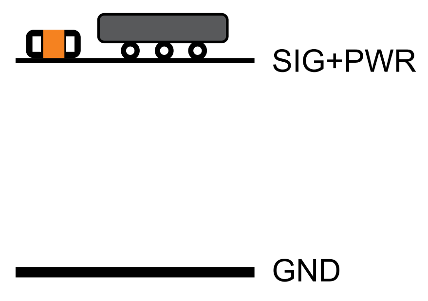 |  |
|---|---|---|
| 4 | 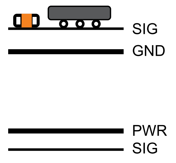 |  |
| 4 |  |  |
| 4 |  |  |
| 6 | 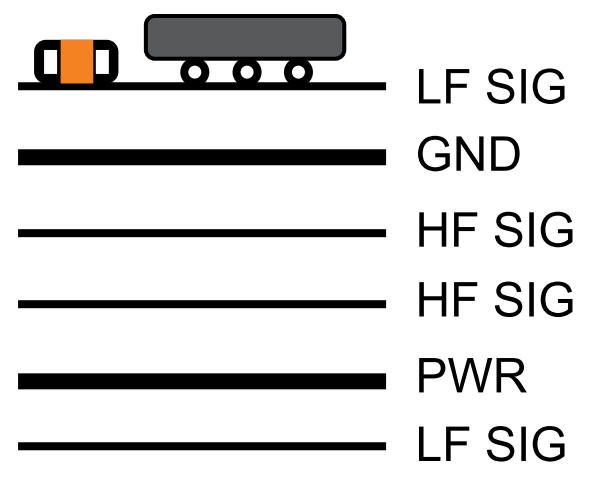 |  |
| 6 | 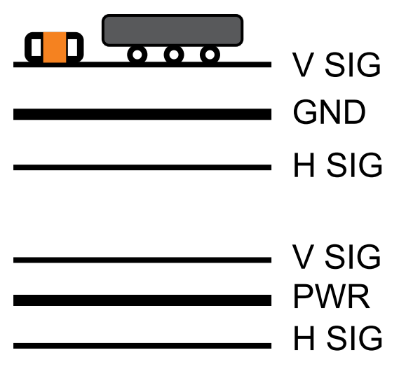 |  |
The thickness of the conductive copper layers
The next important parameter of the printed circuit board is the thickness of the conductive copper layers, which is determined, first of all, by the required minimum clearance and minimum width of the conductor, as well as the maximum current flowing through the conductor. The thinner the conductive layer, the smaller the topological pattern can be obtained and the lower the limiting current can withstand the printed track (ceteris paribus - the width of the conductor, the frequency of the current, heat sink, etc.). The requirement for minimum clearance and conductor width arises from the trace density of the printed circuit board. Another limitation is usually the topology of the recommended footprint of one or more of the applicable chips. Practice shows that when it is necessary to reduce the minimum clearance requirements, the geometry of the recommended seat can be varied within certain limits without prejudice to soldering. At most manufacturers of printed circuit boards, there are standard topological standards and higher (the so-called "5th accuracy class"). The transition to the 5th accuracy class usually leads to a rise in the cost of the printed circuit board by 1.5-2 times, hence it may be necessary to think about the possibility of adjusting the topology as many times to reduce the requirements for standards.
Literature
[1] Ott HW Electromagnetic Compatibility Engineering. Wiley, 2009. The
article was first published in the journal Components and Technologies 2017, No. 12. The publication on Geektimes has been agreed with the editorial staff of the journal.