How to make PCIe friends with 10-meter copper cables and 100-meter optics
Good afternoon! My name is Anton. At YADRO, I do hardware development.
At the end of the review article about the history and development of PCI Express, Alexei mentioned our own adapter for external connection of PCI Express (hereinafter for short - PCIe) devices via cable. Today I will tell you how we tested and debugged it to work correctly with different types and lengths of cable connections.
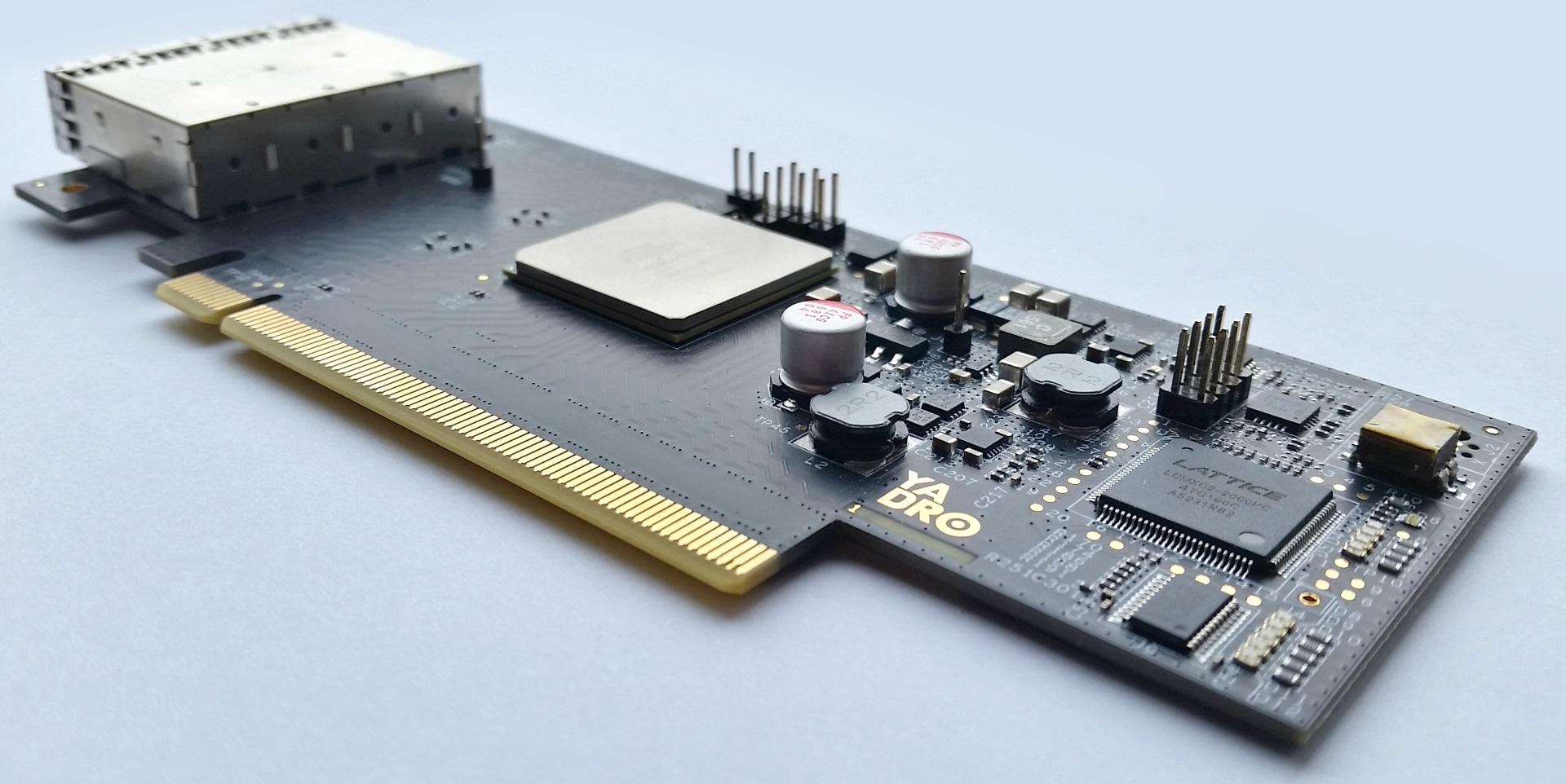
The adapter was designed to connect the components of our systems to each other via the PCIe bus via cable. At the time of development, the existing ready-made solutions for this did not suit us for a number of reasons - some did not support the Gen3 speeds, some used cables that we considered unpromising, etc.
Next I will tell you what problems we encountered (and still encounter) when working with our adapter. But in order to better understand the meaning, we first delve into the theoretical aspects of the interaction of PCIe devices.
I will make a reservation - the description below applies generally to PCIe, but as part of this article for specifics, I used the terminology from the PLX documentation, since our adapter works on a chip of this manufacturer. For other manufacturers, similar methods and entities may be called differently, which does not change the essence.
PCIe devices have an equalizer in the receiving and transmitting paths. Equalizer parameters can and should be changed (tuned) in order to obtain a reliable (BER <10 -12 ) connection.
PCIe transmitters have the following equalizer parameters that can be controlled:
So that the word “cursor” does not flicker constantly - further I will use the first versions of the names of these parameters.
These parameters determine the relationship between the amplitudes of the signal in the time domain:
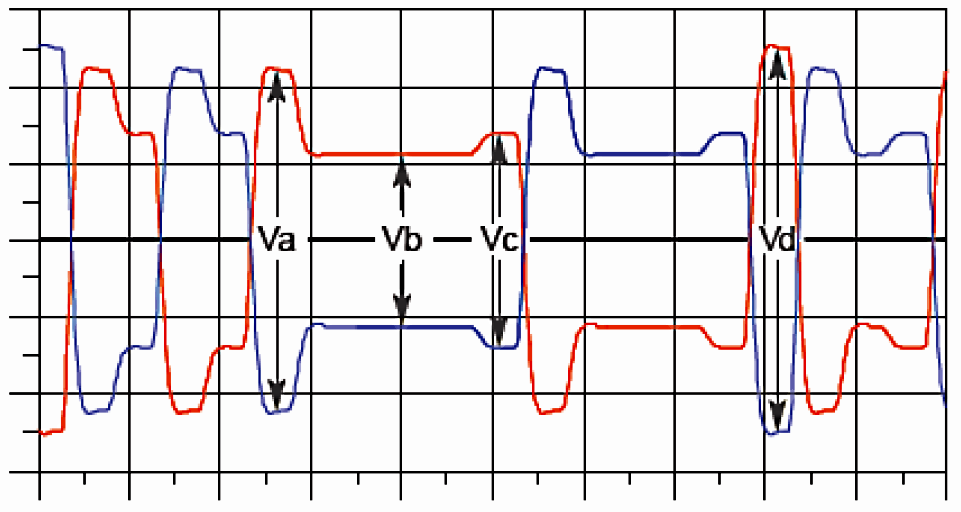
The De-emphasis coefficient determines the Vb / Va ratio, the Pre-shoot coefficient is responsible for the Vc / Vb ratio , and Main is, by and large, the span between the maximum value taking into account pre-shoot and the minimum taking into account de-emphasis (span between short top shelf and long bottom) or vice versa.
If you don’t go too deep into technical details - De-emphasis enhances the amplitude of the transmitted bit depending on the value of the previous bit, and Pre-shoot - does the same depending on the value of the next bit. Main determines the signal swing as a whole.
The values of Main, De-emphasis and Pre-shoot are set by coefficients from 0 to 63. The sum of all coefficients should be 63. That is, if you set Pre-shoot = 6 (3.5 dB), and De-emphasis = 13 (-6 dB ), only 44 will remain on Main. Thus, the signal energy is redistributed between the HF (switching bits) and LF (several 1 or 0 in a row) components.
Looking ahead, I’ll say: for a 10-meter cable, in our case, the optimal values are 63 on Main and zero on Pre-shoot and De-emphasis, or 55-57 on Main with a small Pre-shoot value. That is, at such a cable length, the signal attenuates so that the receiver is no longer up to the edges - it simply cannot recognize the presence of a signal in the line.
When a signal arrives at the receiver, the following tools are sequentially used:
ATT transfer function - almost uniform signal attenuation over the entire frequency range:
The CTLE transfer function is a significant boost in the HF region:
Typically, ATT and CTLE operate in antiphase - low ATT values are accompanied by high CTLE values. That is, the receiver first scales the input signal to an acceptable level, and then pumps the RF component, which undergoes the greatest attenuation in the process of following the channel.
If you have to adjust the coefficients by hand, you need to keep in mind that weak attenuation (and as a result, an overly open "eye") can lead to a glut in the receiving path. And too great a value of BOOST - leads to amplification of RF noise caused, for example, by crosstalk. In general - you do not need to twist these handles to the maximum.
Again, looking ahead, in the case of a 10-meter cable, the ATT is calibrated at 0x0F - the maximum value that means no attenuation. And CTLE in the region of 0x09 - a fairly serious increase in treble. That is, at these distances the signal attenuates so that here just the knobs have to be twisted almost to the maximum.
PCIe Gen3 differs fundamentally from Gen2 and Gen1 in that an iterative phase is present during training, during which the parameters of the receiving and transmitting paths are adjusted. A very large training process is as follows:
The mechanism of such informational interaction of connection partners is called Backchannel Tuning.
At the time of the first inclusion, we, of course, did not conduct any tests (and who conducts them?). We hooked the two adapters with a copper cable, and saw a blinking light bulb. Then, using the lspci command, we checked that the remotely connected PCIe switch is visible in the PCIe tree of the system, and the parameters of the established connection correspond to the expected ones, i.e. x4 / x8 / x16 (depending on the configuration) at a speed of 8 GT / s.
Next, we began to study in more detail the quality of the connection. For half-meter and three-meter cables, BER was zero. There were difficulties with 10-meter cables, and they had to be thoroughly worked out to solve them.
Link-up at 10 meters happened immediately, but was accompanied by a huge rate of error growth. Data could be transmitted, but very slowly. And no matter how much we played with TX PRESETS, no matter how tuned the receiver, nothing helped. We decided to enable DFE. And ... nothing happened.
Further research led us to the fact that DFE has two operating modes - the so-called EDFE (Edge DFE), whose purpose is to expand the "eye" of the signal along the time axis, and the test mode CDFE (Central DFE), whose purpose is to increase the opening of the "eyes" along the amplitude axis.
EDFE did not help us.
The CDFE of the Capella 1 PLX family is turned on by a mysterious painting of unknown registers - very similar to entering some kind of code sequence. The essence of its manufacturer is not disclosed. But he helped us quite tangibly - the BER from 120k x 10 -12 dropped to 1.5kx 10 -12 . But this is still above the level required by the standard, and we continued to bang our head against the wall, sorting through various parameters.
We played with a large number of different parameters, for example, receiver sensitivity, transmitter evaluation time, number of iterations - nothing helped. I must say that the hardware of the PLX switch along with specialized software allows you to get an eye diagram image for each line. But for us, this function turned out to be useless, since the data capture point used to construct the eye diagram is located before the DFE block - that is, we do not see what DFE does with the signal. And before DFE, we have not just a closed "eye", but literally 0 in the line (although link-up still works).
As a result, we have become demoralized. We realized that the aircraft carrier could not be stopped, and decided to look for a button - we took up another problem, which was temporarily postponed until then. The problem was that in general, link-up sometimes didn’t happen on all lines. This indicated that there were some problems with the initial connection at the Gen1 speed - since it was at this stage that the lines were rejected.
We turned on (again a test) Gen1 calibration mode (it is not provided for in standard work). Gen1 stopped working at all (apparently, it couldn’t reach an acceptable BER level) - but then we saw what parameters the receiver was trying to link-up to, where it was aiming, and suddenly realized that they were in another universe with respect to the standard ones. For the sake of interest, we took and interrupted the standard 0x09 / 0x05 at 0x09 / 0x0F (turned off the attenuator for Gen1).
And we got not just a stable link-up Gen1, but also much more pleasant BER values for Gen3 - 0.3 x 10 -12 , which already fits into the standard framework. How the Gen1 receptor pathway is associated with Gen3 - the manufacturer does not say. But so it works.
We had to tinker with optical cables separately due to the PCIe features, but compared to the work of punching 10-meter copper cables, it was easier.
In a nutshell, the situation is different with optics than with copper.
Receiver Detect
After the start of operation, PCIe transmitters begin to check the line for load. They do this by analyzing the signal reflected from the opposite end of the line. If the line is not terminated by the receiver, the transmitter recognizes and rejects this line.
The problem with optical receivers is that often their termination does not meet the PCIe specification, they can be terminated to a different impedance or not be terminated to ground at all. Having seen this, the transmitter may decide that it does not have a receiver - and not begin the procedure for establishing a connection. For correct operation with optics, it is recommended to mask the signals of the Receiver Detect block. In other words, force the transmitter to “see” the receiver.
Electrical Idle Status (hereinafter - IDLE)
Downtimes in a non-modulation line caused, for example, by a transition to a low power state, can lead to oversaturation of the PIN diode and cause problems when exiting this state. The receiver may mistakenly accept the noise caused by the transient state of the optical receiver as exiting the IDLE state and tune to the wrong frequency. This will lead to rejection of this line during the procedure of establishing a connection in the future.
The picture below shows what the PCIe receiver receives when IDLE happens in line with the optics:
Where there is a "Dead Zone" - there should be a constant signal level. And the value of "Settling time" may have a different value on different lines.
Inferred IDLE mode
When using the Inferred IDLE mode, the receiver analyzes the context of the transmitted data and does not rely on signal levels when determining the entrance to the IDLE state. Using this mode is preferable when using an optical cable, because without him:
On PLX switches, this is the default mode.
Downtrain Disable
In the process of establishing a connection, the receiver tries to catch the connection on the oldest or youngest line. As soon as he does this, the remaining lines have a limited time to complete the training. In view of the reasons described above, setting up different lines can take a very different time, therefore, after establishing a connection on the last line, the others may simply not be in time and will be rejected. It is recommended that the receiver is prevented from establishing a connection below the specified channel width so that it tries to fully configure all port lines.
Tuning
Optical devices are non-linear, so you cannot rely on the Backchannel Tuning mechanism, since it relies on linear attenuation of the signal when calculating the calibration coefficients of receivers and transmitters. In some cases, it is better to turn it off, and calibrate the parameters of the receivers and transmitters by hand.
In general, there are many parameters that can be controlled to make optics work. To have access to them on the fly, we installed a CPLD chip on the adapter. We started by using all the parameters recommended by the switch manufacturer at once - and nothing happened. Then we discovered that we forgot one parameter, namely, turning off the Receiver Detect block.
They turned it on, and the optics came to life.
Then we returned all the parameters except Receiver Detect to the default state. Optics continued to live.
Masking Receiver Detect in no way interferes with the work and passive copper cable. Thus, we got a working configuration on both types of connections.
I must say that sometimes errors appear in the channel, but the frequency of their occurrence is within the standard. And since tuning as applied to optics, we have not yet dealt with in essence, that is, a strong belief that these errors can be defeated.
Researchers on this issue frighten developers a lot and that because of the large production scatter between the cables it is quite problematic to assemble the x8 connection from two x4 cables, and even more so x16 - from 4 x4 cables. Therefore, with the goal of minimizing these risks, we aligned all the tracks on the board with 100 ps. I don’t know if this has any significance, but we did not have problems with the aggregation of four x4 to x16 links on 100-meter optics.
The cable connection we use (both optical and copper) has the following pitfalls:
Klok
In general, PCIe klok is necessary for normal operation of the channel. But the switches we use are SRIS-compatible. SRIS - Separate Reference Independent Spread. In simple words, they can not only work on different shreds, but these shreds can be SSC.
In this case, normal operation is possible only when connecting two SRIS devices. Performance is not guaranteed when the host processor is directly connected to anything without a lock. Although we observed normal operation when the x86 processor had a cableless connection with the PLX device, provided that the host used on the host processor does not use SSC. This is called SRNS - Separate Reference No Spread.
Our adapter has its own subsystem of shreds, which allows you to both clock everything from the system PCIe shred and work on your own, which in turn can be either SSC or non-SSC.
We did not like the work on the systemlock as a result of testing, although we cherished the hope of working only on it, and remove the rest of the circuitry related to the chips.
Work on own shred of both nonSSC and SSC is stable and reliable when using passive copper cables up to 4 meters, as well as with an optical cable. For a 10-meter copper cable, normal channel operation is currently achieved only with nonSSC clock.
I2C
This is an optional interface, and in general we lose nothing without passing it on. It was just necessary to note that we are not transferring it.
Other sideband
Lack of it entails, for example, such problems:
and other similar things that can be called a common word - synchronization.
These problems require a more global approach and will be solved at the stage of system integration. At the moment, we make sure that we turn on the host system after the target so that the host system can normally enumerate PCIe devices in the standard boot process.
Also, this problem is not relevant when using NTB.
Actually, as Alexei already mentioned in a previous article , we will have an adapter in two versions. The second option will not be equipped with a PCIe switch, but will have a simple redriver. This is a cheaper option, suitable for those cases when port bifurcation is not needed.
I must also say that in our relatively inexpensive PCIe switch chip there is no DMA controller. Therefore, if you connect these two adapters together, the speed will be low and will greatly depend on the processor - on how and with what data blocks it operates. If there is at least one DMA controller adapter - the real speed usually is about 50-60% of the physically available limit - that is, about 8-9 GB / s in one direction. Although, of course, a single data transfer operation can happen at a speed of 16 GB / s. PR-schiki like to write 32 GB / s - this is the physical limit in both sides. But the information interaction on the PCIe bus is usually two-way - the Completion Response sends the target for each transaction. So work with a performance of 32 GB / s seems to me very doubtful.
Naturally, this choice of chip is quite rational: in the planned use cases, at least one adapter will necessarily have a DMA controller. Therefore, paying in half for a more advanced PCIe switch chip with built-in DMA support in our case makes no sense.
We do not plan to sell this adapter as a separate product - this is not our area of activity, we will put it only in integrated solutions from our own equipment. If you need a similar adapter with a DMA controller, then such solutions have appeared on the market. You can look at Dolphin PXH830 (HBA) or PHX832 (Host / Target), although these adapters have slightly different parameters.
The model 830 has the ability to split ports into 2 x8 or 1 x16, our 4 x4 mode is not. Model 832 can work in 4 x4 mode, but only with passive cables up to 5 m. For both models, support for optical cables up to 100 m in length is announced.
As a result, the adapter worked with copper cables up to 10 meters and with optical cables up to 100 meters, BER in both cases is within the acceptable standard limits. We plan to release a second revision with a reduced number of layers, improve the layout, test and play with fine-tuning the parameters for optics for additional polishing of the results.
Thanks for attention.
At the end of the review article about the history and development of PCI Express, Alexei mentioned our own adapter for external connection of PCI Express (hereinafter for short - PCIe) devices via cable. Today I will tell you how we tested and debugged it to work correctly with different types and lengths of cable connections.
The adapter was designed to connect the components of our systems to each other via the PCIe bus via cable. At the time of development, the existing ready-made solutions for this did not suit us for a number of reasons - some did not support the Gen3 speeds, some used cables that we considered unpromising, etc.
Next I will tell you what problems we encountered (and still encounter) when working with our adapter. But in order to better understand the meaning, we first delve into the theoretical aspects of the interaction of PCIe devices.
I will make a reservation - the description below applies generally to PCIe, but as part of this article for specifics, I used the terminology from the PLX documentation, since our adapter works on a chip of this manufacturer. For other manufacturers, similar methods and entities may be called differently, which does not change the essence.
Tuning
PCIe devices have an equalizer in the receiving and transmitting paths. Equalizer parameters can and should be changed (tuned) in order to obtain a reliable (BER <10 -12 ) connection.
Transmitter tuning
PCIe transmitters have the following equalizer parameters that can be controlled:
- De-emphasis or post-cursor
- Pre-shoot or pre-cursor
- Main or cursor
So that the word “cursor” does not flicker constantly - further I will use the first versions of the names of these parameters.
These parameters determine the relationship between the amplitudes of the signal in the time domain:
The De-emphasis coefficient determines the Vb / Va ratio, the Pre-shoot coefficient is responsible for the Vc / Vb ratio , and Main is, by and large, the span between the maximum value taking into account pre-shoot and the minimum taking into account de-emphasis (span between short top shelf and long bottom) or vice versa.
If you don’t go too deep into technical details - De-emphasis enhances the amplitude of the transmitted bit depending on the value of the previous bit, and Pre-shoot - does the same depending on the value of the next bit. Main determines the signal swing as a whole.
The values of Main, De-emphasis and Pre-shoot are set by coefficients from 0 to 63. The sum of all coefficients should be 63. That is, if you set Pre-shoot = 6 (3.5 dB), and De-emphasis = 13 (-6 dB ), only 44 will remain on Main. Thus, the signal energy is redistributed between the HF (switching bits) and LF (several 1 or 0 in a row) components.
Looking ahead, I’ll say: for a 10-meter cable, in our case, the optimal values are 63 on Main and zero on Pre-shoot and De-emphasis, or 55-57 on Main with a small Pre-shoot value. That is, at such a cable length, the signal attenuates so that the receiver is no longer up to the edges - it simply cannot recognize the presence of a signal in the line.
Receiver Tuning
When a signal arrives at the receiver, the following tools are sequentially used:
- ATT (attenuator);
- BOOST or CTLE - RF component amplifier;
- DFE - a block that essentially works similar to the de-emphasis / pre-shoot stages of the transmitter (disabled by default), is designed to eliminate intersymbol interference (ISI).
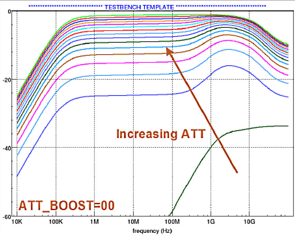
ATT transfer function - almost uniform signal attenuation over the entire frequency range:
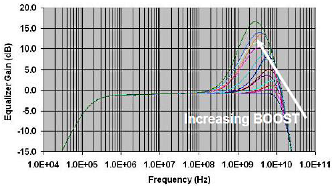
The CTLE transfer function is a significant boost in the HF region:
Typically, ATT and CTLE operate in antiphase - low ATT values are accompanied by high CTLE values. That is, the receiver first scales the input signal to an acceptable level, and then pumps the RF component, which undergoes the greatest attenuation in the process of following the channel.
If you have to adjust the coefficients by hand, you need to keep in mind that weak attenuation (and as a result, an overly open "eye") can lead to a glut in the receiving path. And too great a value of BOOST - leads to amplification of RF noise caused, for example, by crosstalk. In general - you do not need to twist these handles to the maximum.
Again, looking ahead, in the case of a 10-meter cable, the ATT is calibrated at 0x0F - the maximum value that means no attenuation. And CTLE in the region of 0x09 - a fairly serious increase in treble. That is, at these distances the signal attenuates so that here just the knobs have to be twisted almost to the maximum.
PCIe Gen3 Workout
PCIe Gen3 differs fundamentally from Gen2 and Gen1 in that an iterative phase is present during training, during which the parameters of the receiving and transmitting paths are adjusted. A very large training process is as follows:
- It all starts with Gen1. At this stage, there is no tuning, everyone starts with standard values and does not change them in the process. In particular, for the Gen1 receiver, this is ATT = 0x09, CTLE = 0x05.
- The DownStream port tells the Upstream port initial values for the transmitter trim (TX PRESETS) for Gen3 and sets the start values for itself (usually they coincide).
- The upstream port configures its transmitter, and partners go into Gen3 mode. If the quality of the connection does not allow you to get a BER lower than 10 -4 , then everything, nothing works. That is, starting parameter values are often important.
- If link-up occurs, the Downstream port begins to calibrate its receiver and advises the Upstream port to new transmitter settings until it reaches BER
10 -12 . - After this, the same procedure occurs, but vice versa - advises Upstream, and DownStream is calibrated. Well, then happens link-up.
The mechanism of such informational interaction of connection partners is called Backchannel Tuning.
Testing and debugging when working with copper cables
At the time of the first inclusion, we, of course, did not conduct any tests (and who conducts them?). We hooked the two adapters with a copper cable, and saw a blinking light bulb. Then, using the lspci command, we checked that the remotely connected PCIe switch is visible in the PCIe tree of the system, and the parameters of the established connection correspond to the expected ones, i.e. x4 / x8 / x16 (depending on the configuration) at a speed of 8 GT / s.
Next, we began to study in more detail the quality of the connection. For half-meter and three-meter cables, BER was zero. There were difficulties with 10-meter cables, and they had to be thoroughly worked out to solve them.
Link-up at 10 meters happened immediately, but was accompanied by a huge rate of error growth. Data could be transmitted, but very slowly. And no matter how much we played with TX PRESETS, no matter how tuned the receiver, nothing helped. We decided to enable DFE. And ... nothing happened.
Further research led us to the fact that DFE has two operating modes - the so-called EDFE (Edge DFE), whose purpose is to expand the "eye" of the signal along the time axis, and the test mode CDFE (Central DFE), whose purpose is to increase the opening of the "eyes" along the amplitude axis.
EDFE did not help us.
The CDFE of the Capella 1 PLX family is turned on by a mysterious painting of unknown registers - very similar to entering some kind of code sequence. The essence of its manufacturer is not disclosed. But he helped us quite tangibly - the BER from 120k x 10 -12 dropped to 1.5kx 10 -12 . But this is still above the level required by the standard, and we continued to bang our head against the wall, sorting through various parameters.
We played with a large number of different parameters, for example, receiver sensitivity, transmitter evaluation time, number of iterations - nothing helped. I must say that the hardware of the PLX switch along with specialized software allows you to get an eye diagram image for each line. But for us, this function turned out to be useless, since the data capture point used to construct the eye diagram is located before the DFE block - that is, we do not see what DFE does with the signal. And before DFE, we have not just a closed "eye", but literally 0 in the line (although link-up still works).
As a result, we have become demoralized. We realized that the aircraft carrier could not be stopped, and decided to look for a button - we took up another problem, which was temporarily postponed until then. The problem was that in general, link-up sometimes didn’t happen on all lines. This indicated that there were some problems with the initial connection at the Gen1 speed - since it was at this stage that the lines were rejected.
We turned on (again a test) Gen1 calibration mode (it is not provided for in standard work). Gen1 stopped working at all (apparently, it couldn’t reach an acceptable BER level) - but then we saw what parameters the receiver was trying to link-up to, where it was aiming, and suddenly realized that they were in another universe with respect to the standard ones. For the sake of interest, we took and interrupted the standard 0x09 / 0x05 at 0x09 / 0x0F (turned off the attenuator for Gen1).
And we got not just a stable link-up Gen1, but also much more pleasant BER values for Gen3 - 0.3 x 10 -12 , which already fits into the standard framework. How the Gen1 receptor pathway is associated with Gen3 - the manufacturer does not say. But so it works.
Work with optical cables
We had to tinker with optical cables separately due to the PCIe features, but compared to the work of punching 10-meter copper cables, it was easier.
In a nutshell, the situation is different with optics than with copper.
What are the differences from copper
Receiver Detect
After the start of operation, PCIe transmitters begin to check the line for load. They do this by analyzing the signal reflected from the opposite end of the line. If the line is not terminated by the receiver, the transmitter recognizes and rejects this line.
The problem with optical receivers is that often their termination does not meet the PCIe specification, they can be terminated to a different impedance or not be terminated to ground at all. Having seen this, the transmitter may decide that it does not have a receiver - and not begin the procedure for establishing a connection. For correct operation with optics, it is recommended to mask the signals of the Receiver Detect block. In other words, force the transmitter to “see” the receiver.
Electrical Idle Status (hereinafter - IDLE)
Downtimes in a non-modulation line caused, for example, by a transition to a low power state, can lead to oversaturation of the PIN diode and cause problems when exiting this state. The receiver may mistakenly accept the noise caused by the transient state of the optical receiver as exiting the IDLE state and tune to the wrong frequency. This will lead to rejection of this line during the procedure of establishing a connection in the future.
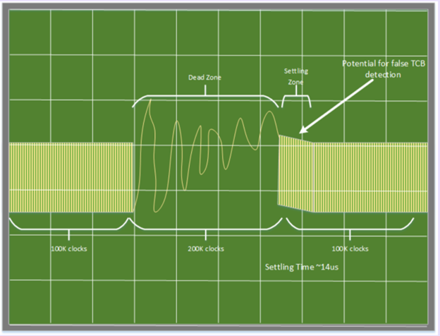
The picture below shows what the PCIe receiver receives when IDLE happens in line with the optics:
Where there is a "Dead Zone" - there should be a constant signal level. And the value of "Settling time" may have a different value on different lines.
Inferred IDLE mode
When using the Inferred IDLE mode, the receiver analyzes the context of the transmitted data and does not rely on signal levels when determining the entrance to the IDLE state. Using this mode is preferable when using an optical cable, because without him:
- transients in the optical receiver can initiate an erroneous entry into the IDLE state and subsequent stages of the state machine LTSSM.
- transition to IDLE state by one partner, may not be recognized by the second partner.
On PLX switches, this is the default mode.
Downtrain Disable
In the process of establishing a connection, the receiver tries to catch the connection on the oldest or youngest line. As soon as he does this, the remaining lines have a limited time to complete the training. In view of the reasons described above, setting up different lines can take a very different time, therefore, after establishing a connection on the last line, the others may simply not be in time and will be rejected. It is recommended that the receiver is prevented from establishing a connection below the specified channel width so that it tries to fully configure all port lines.
Tuning
Optical devices are non-linear, so you cannot rely on the Backchannel Tuning mechanism, since it relies on linear attenuation of the signal when calculating the calibration coefficients of receivers and transmitters. In some cases, it is better to turn it off, and calibrate the parameters of the receivers and transmitters by hand.
In general, there are many parameters that can be controlled to make optics work. To have access to them on the fly, we installed a CPLD chip on the adapter. We started by using all the parameters recommended by the switch manufacturer at once - and nothing happened. Then we discovered that we forgot one parameter, namely, turning off the Receiver Detect block.
They turned it on, and the optics came to life.
Then we returned all the parameters except Receiver Detect to the default state. Optics continued to live.
Masking Receiver Detect in no way interferes with the work and passive copper cable. Thus, we got a working configuration on both types of connections.
I must say that sometimes errors appear in the channel, but the frequency of their occurrence is within the standard. And since tuning as applied to optics, we have not yet dealt with in essence, that is, a strong belief that these errors can be defeated.
Researchers on this issue frighten developers a lot and that because of the large production scatter between the cables it is quite problematic to assemble the x8 connection from two x4 cables, and even more so x16 - from 4 x4 cables. Therefore, with the goal of minimizing these risks, we aligned all the tracks on the board with 100 ps. I don’t know if this has any significance, but we did not have problems with the aggregation of four x4 to x16 links on 100-meter optics.
Common problems
The cable connection we use (both optical and copper) has the following pitfalls:
- the reference clock signal is not transmitted in the line (hereinafter referred to as the clock);
- I2C is not transmitted in the line;
- PERST #, PRSNT # and other sideband are not transmitted in the line.
Klok
In general, PCIe klok is necessary for normal operation of the channel. But the switches we use are SRIS-compatible. SRIS - Separate Reference Independent Spread. In simple words, they can not only work on different shreds, but these shreds can be SSC.
SSC
Spread Spectrum Clocking is a modulation of the clock frequency in the interval 0 to -5000 ppm with a frequency of 30–33 kHz. It is used to reduce EMR. In this case, the radiation power is smeared in the spectrum, since the frequency of the block constantly floats a little.
In this case, normal operation is possible only when connecting two SRIS devices. Performance is not guaranteed when the host processor is directly connected to anything without a lock. Although we observed normal operation when the x86 processor had a cableless connection with the PLX device, provided that the host used on the host processor does not use SSC. This is called SRNS - Separate Reference No Spread.
Our adapter has its own subsystem of shreds, which allows you to both clock everything from the system PCIe shred and work on your own, which in turn can be either SSC or non-SSC.
We did not like the work on the systemlock as a result of testing, although we cherished the hope of working only on it, and remove the rest of the circuitry related to the chips.
Work on own shred of both nonSSC and SSC is stable and reliable when using passive copper cables up to 4 meters, as well as with an optical cable. For a 10-meter copper cable, normal channel operation is currently achieved only with nonSSC clock.
I2C
This is an optional interface, and in general we lose nothing without passing it on. It was just necessary to note that we are not transferring it.
Other sideband
Lack of it entails, for example, such problems:
- the inability to synchronously reset the entire PCIe tree, as it happens when all PCIe devices are in one box;
- problems with the sudden disappearance and addition of devices on the PCIe bus;
and other similar things that can be called a common word - synchronization.
These problems require a more global approach and will be solved at the stage of system integration. At the moment, we make sure that we turn on the host system after the target so that the host system can normally enumerate PCIe devices in the standard boot process.
Also, this problem is not relevant when using NTB.
Options and analogues
Actually, as Alexei already mentioned in a previous article , we will have an adapter in two versions. The second option will not be equipped with a PCIe switch, but will have a simple redriver. This is a cheaper option, suitable for those cases when port bifurcation is not needed.
I must also say that in our relatively inexpensive PCIe switch chip there is no DMA controller. Therefore, if you connect these two adapters together, the speed will be low and will greatly depend on the processor - on how and with what data blocks it operates. If there is at least one DMA controller adapter - the real speed usually is about 50-60% of the physically available limit - that is, about 8-9 GB / s in one direction. Although, of course, a single data transfer operation can happen at a speed of 16 GB / s. PR-schiki like to write 32 GB / s - this is the physical limit in both sides. But the information interaction on the PCIe bus is usually two-way - the Completion Response sends the target for each transaction. So work with a performance of 32 GB / s seems to me very doubtful.
Naturally, this choice of chip is quite rational: in the planned use cases, at least one adapter will necessarily have a DMA controller. Therefore, paying in half for a more advanced PCIe switch chip with built-in DMA support in our case makes no sense.
We do not plan to sell this adapter as a separate product - this is not our area of activity, we will put it only in integrated solutions from our own equipment. If you need a similar adapter with a DMA controller, then such solutions have appeared on the market. You can look at Dolphin PXH830 (HBA) or PHX832 (Host / Target), although these adapters have slightly different parameters.
The model 830 has the ability to split ports into 2 x8 or 1 x16, our 4 x4 mode is not. Model 832 can work in 4 x4 mode, but only with passive cables up to 5 m. For both models, support for optical cables up to 100 m in length is announced.
What's next?
As a result, the adapter worked with copper cables up to 10 meters and with optical cables up to 100 meters, BER in both cases is within the acceptable standard limits. We plan to release a second revision with a reduced number of layers, improve the layout, test and play with fine-tuning the parameters for optics for additional polishing of the results.
Thanks for attention.