The performance of dynamic RAM and the ridiculous idea of how to increase it
A bit of history
At the dawn of computing technology, dynamic memory worked for itself at the processor frequency. My first computer experience was with the ZX Spectrum computer clone. The Z80 processor processed instructions on average for 4 clock cycles per operation, while two clock cycles were used to perform dynamic memory regeneration, which gives us at a frequency of 3.5 MHz, no more than 875,000 operations per second.
However, after some time, the processor frequencies reached a level where dynamic memory could no longer cope with the load. To compensate for this, an intermediate link was introduced in the form of a cache memory, which made it possible to smooth out the difference in processor speed and main memory due to operations performed on a small amount of data.
Let's look at what the RAM of the computer is now, and what can be done with it to increase the speed of the computer system.
Briefly about static and dynamic memory
The memory is built in the form of a table consisting of rows and columns. In each cell of the table there is an information bit (we discuss semiconductor memory, however, many other implementations are built on the same principle). Each such table is called a “bank." A chip / module can accommodate several banks. The set of memory modules is projected into the linear address space of the processor depending on the bit depth of individual elements.
A static memory cell is built on the basis of a trigger, which is usually in one of the stable states “A” or “B” (A =! B). The minimum number of transistors for one cell is 6 pieces, while the complexity of the trace in the cells apparently does not allow making 1 gig of static memory modules, at the price of a regular module of 8 gigabytes.
A dynamic memory cell consists of one capacitor responsible for storing information and one transistor responsible for isolating the capacitor from the data bus. Moreover, not a mounted electrolyte is used as a capacitor, but the parasitic capacitance pn of the junction between the “substrate” and the transistor electrode (especially for these purposes it is increased, usually they try to get rid of it). The disadvantage of a capacitor is the leakage current (both in it and in the key transistor), which is very difficult to get rid of, in addition, with an increase in temperature, it increases, which leads to the likelihood of distortion of the stored information. To maintain reliability, “regeneration” is used in dynamic memory; it consists in periodically updating the stored information at least for a specified period during which the information retains a reliable value.
Otherwise, the principle of operation is identical and consists in the following:
- the initial retrieval of a memory row leads to access to all its contents placed in a buffer row with which further work is going on, or multiplication of access to columns occurs (old, slow approach);
- the requested data is transferred to the main device (usually the CPU), or the specified cells are modified during the write operation (there is a slight difference, direct modification of the selected row cell is possible for static memory, the buffer line is modified for dynamic memory, and only then write back the contents of the entire line in a special loop);
- closing and changing the memory line is also different for different types of memory, for static it is possible to immediately change the line if the data has not changed, for dynamic memory it is necessary to write the contents of the buffer line into place, and only then you can select another line.
If at the dawn of computing technology, each read or write operation ended with a full memory cycle:
- line selection;
- operation of reading / writing from the cell;
- change / reselection of a line.
The modern operation of working with microchips "synchronous memory a la DDRX" is as follows:
- line selection;
- operations of reading / writing cells of a row in groups of 4-8 bits / words (multiple access within one row is allowed);
- closing the line with recording information in place;
- change / reselection of a line.
This solution allowed us to save data access time when, after reading the value from cell “1”, you need to access cells “2, 3, 4, or 7” located on the same line, or immediately after the read operation, you need to write back the changed value .
Read more about the operation of dynamic memory in conjunction with the cache
The memory controller (in the chipset or integrated in the processor) sets the block address and line number (the upper part of the block address) in the microchip / memory module. The corresponding block is selected (further work within the framework of one block will be considered) and the resulting “binary number” is decoded into the positional address of the string, after which information is transferred to the buffer, from which data is subsequently accessed. The time in cycles required for this operation is called tRCD and is displayed in the second place in the “9-9-9 / 9-9-9-9-27” schemes.
After the row is activated, you can access the "columns" for this, the memory controller transmits the address of the cell in the row, and after a while "CL" (indicated in the above designated scheme "xxxx" in 1 place), data begins to be transmitted from the memory chip to the processor (why in the plural? because the cache interferes here) in the form of a packet of 4-8 bits (for a single chip) in the cache line (the size depends on the processor, a typical value of 64 bytes is 8 words of 64 bits, but there are and other meanings). After a certain number of clock cycles required to transfer the data packet, you can form the next request to read data from other cells of the selected row, or issue a command to close the line which is expressed as tRP specified as the third parameter from “xxxx ... ". While closing a row, data from the buffer is written back to the line of the block, after the end of the recording, you can select another line in this block. In addition to these three parameters, there is a minimum time during which the line must be active “tRAS”, and a minimum time for a full cycle of working with the line separating the two commands for activating the line (affects random access).
grossws April 19, 2016 at 12:40
CL - CAS latency, tRCD - RAS to CAS delay, tRP - row precharge, CAS - column address strobe, RAS - row address strobe.The speed of semiconductor technology is determined by the delays of the circuit elements. In order to get reliable information at the output, it is necessary to wait a certain time for all the elements to take a steady state. Depending on the current state of the memory bank, the data access time changes, but in general, the following transitions can be characterized:
If the block is at rest (there is no active row), the controller issues a row selection command, as a result, the binary row number is converted to a position number, and reading the contents of the string during the "tRCD".
After the contents of the line have been read into the buffer zone, you can issue a column selection command, according to which the binary number of the column is converted to a position number, during the “CL” time, but depending on the alignment of the lower addresses, the order of bit transmission may change.
Before changing / closing the line, it is necessary to write the data in place, since during the reading, the information was actually destroyed. The time required to restore the information in the line "tRP".
According to the full specification for dynamic memory, there are many more time parameters that determine the sequence and delay of changes in control signals. One of these is tRCmin, which defines the minimum time for a full line cycle, including: line selection, data access, and writeback.
The RAS signal determines the fact of issuing the address of the string;
The CAS signal determines whether a column address has been issued.
If earlier all control was shifted to the side of the memory controller and controlled by these signals, now there is a command mode, when a command is issued to the module / microcircuit, and after a while data is transferred. It is better to get acquainted in more detail in the specification of the standard, for example DDR4 .
If we talk about working with dram in general, then during mass reading it usually looks like this:
set the address of the line,
set RAS (and took it out after a measure),
wait for tRCD,
set the address of the column with which we read (and each next measure we set the next column number ),
set CAS,
waited for CL, started reading data,
removed CAS, read the rest of the data (another CL cycles).
During the transition, the next row is not precharge (RAS + WE), tRP is waited, RAS is executed with the address of the line set, and then reading is performed as described above.
The latency of reading a random cell naturally follows from the above: tRP + tRCD + CL.In reality, it depends on the previous state of the “memory bank" that is being accessed.
It must be remembered that DDR RAM has two frequencies:
- the main clock frequency that determines the rate of transmission of commands and timings;
- effective data transfer frequency (double clock frequency, which marks the memory modules).
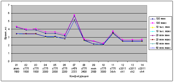
The integration of the memory controller increased the performance of the memory subsystem due to the rejection of the intermediate transmission link. An increase in memory channels will require taking this into account on the application side, for example, four-channel mode with a certain file location does not give a performance gain (configuration 12 and 14).
Processing a single linked list item with different steps (1 step = 16 bytes)

Now a little math
Processor: processor operating frequencies now reach 5 GHz. According to the manufacturers, circuitry solutions (conveyors, predictions and other tricks) allow you to execute one instruction per cycle. To round off the calculations, we take the value of the clock frequency of 4 GHz which will give us one operation in 0.25 ns.
RAM: take for example the RAM of the new format DDR4-2133 with a timing of 15-15-15.
Given:
processor
Fact = 4 GHz
Tact = 0.25 ns (part-time execution of one operation is “conditional”)
RAM DDR4-2133
Fact = 1066 MHz
Fdata = 2133 MHz
tact = 0.94 ns
tdate = 0.47 ns
SPDmax = 2133 MHz * 64 = 17064 MB / s (data transfer rate)
tRCmin = 50 ns (minimum time between two row activations)
Data acquisition time
From registers and cache, data can be provided during the working cycle (registers, level 1 cache) or with a delay of several processor cycles for the cache of the 2nd and 3rd levels.
For RAM, the situation is worse:
- row selection time is: 15 clk * 0.94 ns = 14 ns
- time to get data from the column selection command: 15 clk * 0.94 ns = 14 ns
- row closing time: 15 clk * 0.94 ns = 14 ns (who would have thought)
It follows that the time between a command requesting data from a memory location (if it didn’t get into the cache) can vary:
14 ns - the data is in the already selected line;
28 ns - data is in an unselected row, provided that the previous row is already closed (block in idle state);
42-50 ns - the data is on another line, while the current line needs to be closed.
The number of operations that the processor (mentioned above) can perform during this time is from 56 (14 ns) to 200 (50 ns line breaks). Separately, it is worth noting that by the time between the column selection command and the receipt of the entire data packet, a cache line load delay is added: 8 packet bits * 0.47 ns = 3.76 ns. For the situation when the data will be available to the “program” only after the cache line has been loaded (who knows what and how the developers of the processors have screwed it up, the memory allows specifying the necessary data ahead), we get up to 15 missed clock cycles.
As part of one work, I conducted a study of the speed of memory, the results showed that it is possible to completely “utilize” the memory bandwidth only in sequential memory access operations, in case of random access, the processing time is increased (using the linked list from a 32-bit pointer as an example) and three double words, one of which is updated) from 4-10 (sequential access) to 60-120 ns (line break), which gives a difference in processing speed of 12-15 times.
Data processing speed
For the selected module, we have a peak throughput of 17064 MB / s. That for a frequency of 4 GHz makes it possible to process 32-bit words per cycle (17064 MB / 4000 MHz = 4.266 bytes per cycle). The following restrictions are imposed here:
- without explicit planning for loading the cache, the processor will be forced to stand idle (the higher the frequency, the more the kernel just waits for data);
- in the cycles "reading modification writing" the processing speed is reduced by half;
- multi-core processors will share memory bus bandwidth between cores, and for a situation when there will be competing requests (degenerate case), memory performance may deteriorate "200 times (line break) * X cores".
Calculate:
17064 MB / s / 8 cores = 2133 MB / s per core in the optimal case.
17064 MB / s / (8 cores * 200 missed operations) = 10 MB / s per core for a degenerate case.
Translated into operations, we get for an 8-core processor: from 15 to 400 operations for processing a data byte, or from 60 to 1600 operations / clocks for processing a 32-bit word.
In my opinion, somehow slowly. Compared with the DDR3-1333 9-9-9 memory, where the full cycle time is approximately 50 ns, but the timings differ:
- the data access time decreases to 13.5 ns (1.5 ns * 9 ticks);
- the transmission time of a packet of eight words is 6 ns (0.75 * 8 instead of 3.75 ns) and with random access to the memory, the difference in data transfer speed practically disappears;
- The peak speed will be 10 664 MB / s.
Not too far gone. The situation is slightly saved by the presence of “banks” in the memory modules. Each “bank” is a separate memory table which can be accessed separately, which makes it possible to change the line in one bank while reading / writing data from the line of another, by reducing downtime it allows you to “clog” the data bus to the eyeballs in optimized situations.
In fact, ridiculous ideas went here
The memory table contains a specified number of columns equal to 512, 1024, 2048 bits. Given the cycle time for activating rows of 50 ns, we get the potential data exchange rate: “1 / 0.00000005 s * 512 columns * 64 bit word = 81 920 MB / s” instead of the current 17 064 MB / s (163 840 and 327,680 MB / s for rows of 1,024 and 2,048 columns). You will say: “only 5 times (4.8) faster”, to which I will answer: “this is the exchange rate when all competing requests are addressed to the same memory bank, and the available throughput increases in proportion to the number of banks, and the increase in the length of the row of each table (it will require an increase in the length of the operating line), which in turn rests mainly on the speed of the data bus. "
Changing the data exchange mode will require transferring the entire contents of the line to the lower level cache, for which purpose it is necessary to separate the cache levels not only in speed, but also in the size of the line cache. So, for example, by implementing the “length” of the N-level cache line in (512 columns * 64 word size) 32,768 bits, we can increase the total number of cache lines by decreasing the number of comparison operations and increase its maximum size accordingly. But if we make a parallel bus in a cache of this size, we can get a decrease in the frequency of operation, from which we can use a different approach to organizing the cache, if we break the indicated "Jumbo" cache line into blocks along the length of the top cache line and exchange with small portions, this allows you to save the frequency of operation by dividing the access delay into stages: search for the cache line,
As for the direct exchange between the cache and main memory: it is necessary to transfer data at the rate of access to the lines of one bank, or having a certain margin for distributing requests to different banks. In addition, there is a difficulty over time of access to data located in different areas of the row; for sequential transmission, in addition to the initial delay associated with fetching the row, there is a delay in the transmission of data depending on the amount of data "in the packet" and the transmission speed. Even the rambus approach can not cope with the increased load. The situation can be saved by switching to a serial bus (possibly differential), by further reducing the bit depth of the data, we can increase the bandwidth of the channel, I to reduce the time between the transmission of the first and last bit of data, apply split line feed to multiple channels. That will allow you to use a lower clock frequency of one channel.
Let’s estimate the speed of such a channel:
1 / 0.00000005 ns = 20 MHz (line change frequency within one block)
20 MHz * 32 768 bits = 655 360 Mbit / s
For differential transmission with the same data bus size we get:
655 360 Mbit / s / 32 channels = 20,480 Mb / s per channel.
Such a speed looks acceptable for an electric signal (10 Gbit / s for a signal with built-in synchronization of 15 meters is available, why not overpower 20 GB / s with external synchronization of 1 meter), however, a necessary further increase in the transmission speed to reduce the transmission delay between the first and last bit of information may require an increase in bandwidth, with the possible integration of an optical transmission channel, but this is already a question for circuit designers, I have little experience with such frequencies.
and then Ostap suffered
Changing the concept of projecting the cache onto main memory to use “main memory as an intermediate ultra-fast block storage” will allow us to shift the prediction of loading data from the controller circuitry to the processing algorithm (and who better knows where it will break after some time, obviously not to the memory controller), which in turn, will allow you to increase the volume of the cache of the external level, without compromising performance.
If you go further, you can further change the concept of orienting the processor architecture from “switching the context of the actuator” to “working environment of the program”. Such a change can significantly improve code security by defining a program as a set of functions with specified entry points for individual procedures, an accessible region for placing data for processing, and the possibility of hardware control of the possibility of calling a function from other processes. Such a change will also make it possible to use multicore processors more efficiently by eliminating context switching for some threads, and to process events, use a separate thread within the accessible environment of the “process”, which will make it possible to use 100+ nuclear systems more efficiently.
PS: The random use of registered trademarks or patents is random. All original ideas are available for use under the Anthill license agreement.