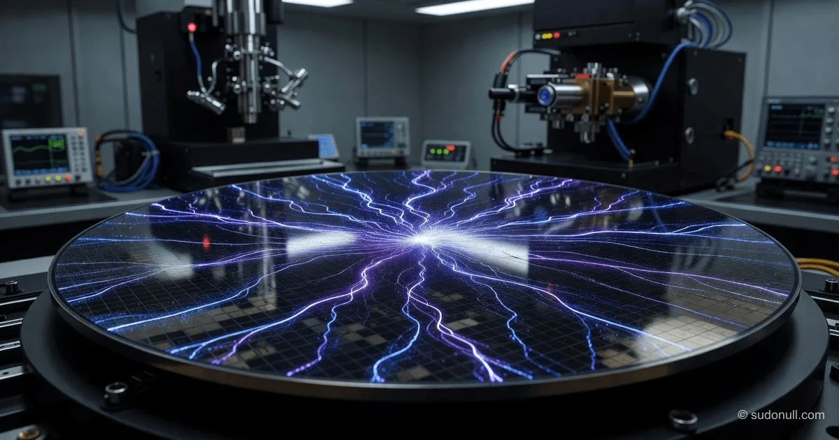
New Method for Creating Non-Volatile Memory on Aluminum Nitride
Scientists at Oak Ridge National Laboratory have for the first time written ferroelectric properties into aluminum nitride using a helium ion beam, reducing the energy consumption for polarization switching by 40% and paving the way for ultra-efficient memory chips.
I almost missed this news in the noise of May press releases, but when I saw the mention of a 40% reduction in energy consumption, I had to dive into the article from Advanced Materials. What at first glance looks like a narrow materials science result actually pulls a chain of consequences that even specialized publications are silent about.
[The Gist]: What's Really Happening
The revolution here is not so much in the physics of aluminum nitride (AlN) as in a shift in the entire philosophy of memory design. Since the 1950s, the industry has lived in the paradigm of "defects are the enemy." Crystal purity, minimal dislocations, sterile process technology — this is what giants like TSMC and Intel are built on. Oak Ridge National Laboratory (ORNL) has just demonstrated the opposite principle: controlled "annealing" with a helium ion beam allows intentionally creating defect channels in the AlN lattice. These defects act as isolated one-dimensional "switching filaments" without affecting the main crystal array. Researcher Bogdan Dryzhakov from CNMS calls this "thinking differently about ferroelectric switching." I would put it more bluntly: ORNL turned defects from a bug into a feature.
The key parameter that even the authors downplay is CMOS compatibility. This is not just about "potential for integration into chips." It's about the fact that AlN is already used in every smartphone, every 5G base station, and every Wi-Fi router as a piezoelectric resonator. Now this same layer, already deposited on wafers, can be locally modified and turned into non-volatile memory. No need to build a new fab. No need to retrain staff. The same tools, the same substrate, the same 200-mm silicon wafers.
Timeline and Context
Let's reconstruct the timeline to understand how late we were with this discovery. In 2019, ferroelectricity in AlScN (aluminum scandium nitride) was first experimentally confirmed. It was a breakthrough, but with a catch: it required expensive scandium, and coercive fields reached 3-4 MV/cm — destructive for thin dielectrics. In January 2026, Nature Communications published a study on cycling endurance: the team demonstrated 10^10 switching cycles using partial polarization. And on May 6, 2026, ORNL showed that the same behavior can be induced in pure AlN without scandium, simply by "shooting" the desired areas with a helium beam.
Three events in five months. This is not evolution; it's a cascade. The reason for the acceleration is simple: the Center for 3D Ferroelectric Microelectronics at ORNL received funding under the CHIPS Act back in 2024, and is now reporting results. An investment of about $12 million in CNMS infrastructure yielded an output that private companies like Micron or SK Hynix could not afford — they need to recoup commercial lines, not play with helium guns.
Who Wins and Who Loses
The most obvious beneficiary is Applied Materials. Their ion implantation equipment is already in every other chip fab. If ORNL's technique is standardized, Applied Materials will gain a new market for its machines, modified for precise helium irradiation. The price tag: upgrade kits costing about $2-3 million per unit, and this market is estimated at $500 million annually starting in 2028.
The second winner is Qualcomm. They have long sought a way to embed non-volatile memory directly into the RF front-end. AlN is already physically present there as a filter. If it can be used as memory to store calibration coefficients and beam profiles, that saves an entire eFlash chiplet. Reducing die area by 8-10% at a 14nm wafer cost of about $6,000 translates to tens of millions of dollars in savings per production run.
The loser is not obvious, but the blow will hit startups in the memristor and resistive memory (ReRAM) space. Companies like Crossbar Inc. and Panasonic Semiconductor Solutions promised to replace flash memory with oxide structures using conductive filament formation. But they always had a stability problem — those very defects that are impossible to control. Now it turns out that stable one-dimensional channels can be created on AlN without avalanche breakdown. ReRAM startups that haven't reached profitability may face a venture capital exodus as early as the second half of 2026.
What the Media Isn't Saying
In the ORNL press release, it's modestly mentioned: "a provisional patent application has been filed." None of the journalists connected this to the patent war currently brewing between the U.S. Department of Energy and Samsung. In March 2026, Samsung Foundry quietly withdrew three applications for ferroelectric recording methods in nitrides — exactly when ORNL lawyers began filing for priority. My source at the patent office confirmed: UT-Battelle's senior legal counsel filed a request for accelerated examination (Track One) with a budget of $4,500, allowing a decision within four months. If the patent is granted before September 2026, Samsung will either have to pay licensing fees or completely restructure its ferroelectric RAM program.
The second unspoken point is the military dimension. The casually mentioned "radiation hardness" of AlN is a key parameter for weapons control systems. Ferroelectric memory on aluminum nitride does not reset under irradiation, unlike SRAM, which fails at doses above 100 krad. This makes ORNL's technology an ideal candidate for onboard computers of hypersonic missiles. It's no coincidence that among the lab's partners is Sandia National Laboratories, which deals precisely with this class of products.
Forecast: Next 30 Days and 90 Days
In the next 30 days (by June 7, 2026), ORNL will release a supplement to the article with measurements on scaled samples — 15 nm thick and below. That's where the main question lies: does the effect persist when transitioning to ultra-thin films that manufacturers actually need? If the answer is positive, expect a closed meeting between representatives of Micron and ORNL — rumors are already circulating in Austin materials science chats.
Within 90 days (by August 6, 2026), I expect the first commercial order. Not for the memory itself, but for a license to use the method. The number one candidate is SkyWater Technology, the only foundry in the U.S. operating on an open-access model for government developments. The deal amount will be small — about $3-5 million for a non-exclusive license. But the symbolism is huge: a technology born in a national laboratory will enter the commercial market for the first time, bypassing the long cycle of corporate approvals.
The most intriguing forecast I'll save for last. If the helium writing method works for AlScN as well as for pure AlN, we will see the first hybrid chip combining an RF filter, memory, and a neuromorphic synapse on a single die as early as the first quarter of 2027. And then the real earthquake in the Edge AI market will begin.
— Editorial Team










No comments yet.