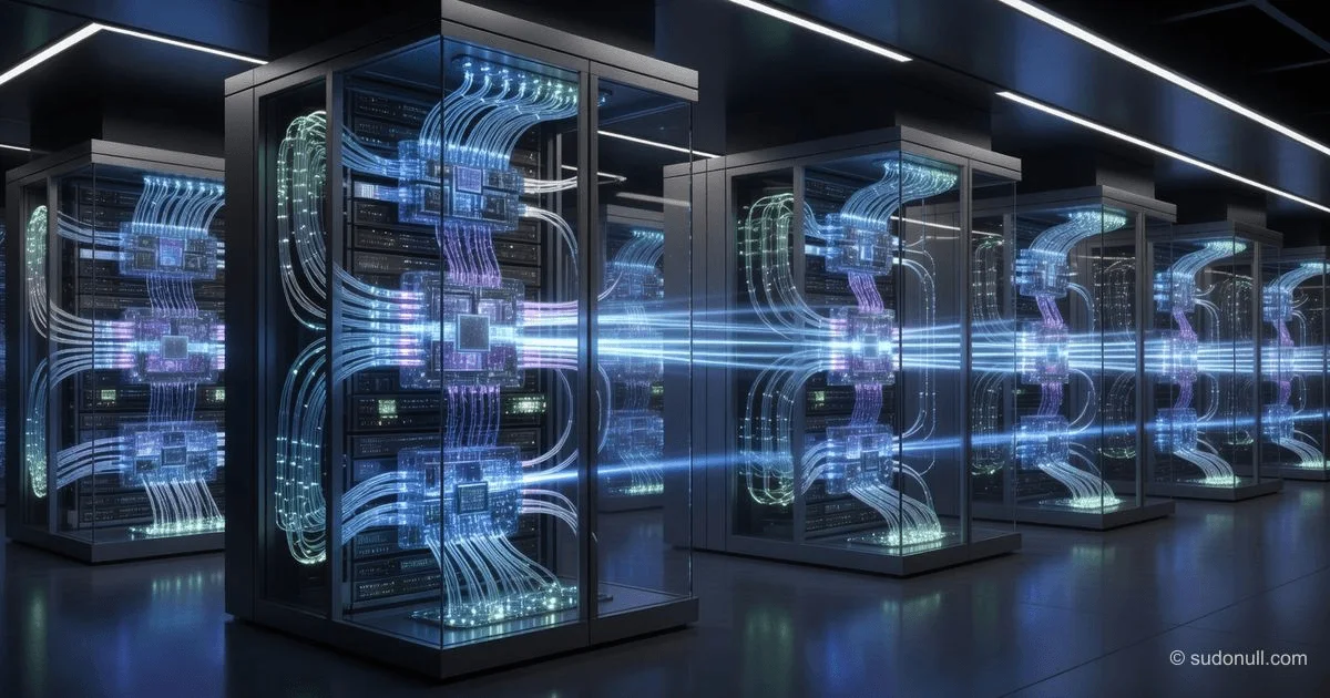
European Scientists Propose Replacing Electrons with Light to Save the Internet from Energy Crisis
A new EU research initiative aims to replace traditional electronics with ultra-efficient photonic technologies for data transmission and processing, which should radically reduce energy consumption in data centers and AI systems amid a projected twofold increase in demand by 2030.
Analytical article based on the provided news and search context:
[Essence]: What is really happening
Behind the loud headlines about "saving the internet with light" lies not so much an academic breakthrough as a tectonic shift in European industrial policy. The new EU research initiative in question is not a single project but a formal umbrella launched at a decisive moment. The essence is that Brussels has moved from a mosaic of scattered laboratory prototypes to a phase of forced industrialization of photonics. We are witnessing not just a theoretical replacement of electrons with photons. We are seeing an attempt to create a fully autonomous European supply chain for photonic chips: from materials (InP, silicon nitride) to packaging. The true goal is not energy efficiency per se, but technological sovereignty. The energy crisis has merely become a convenient pretext for aggressively building competencies bypassing Taiwan and South Korea.
Timeline and context
The situation developed rapidly, especially in the last two days, but its roots go back to 2023–2024. In early 2026, on March 9, it became known that construction had begun in Eindhoven (Netherlands) of the world's first industrial factory for producing photonic chips based on indium phosphide (InP) on 6-inch wafers. The investment amounted to 150 million EUR, the project is being implemented under the auspices of TNO and the PIXEurope consortium as part of the EU Chips Act. The key point here is the transition from laboratory samples to industrial pilot lines.
In parallel, on May 2, 2026, ASML and imec signed a new strategic agreement, formally designed for five years, with a focus on sustainable innovation. Under this partnership, ASML equipment, including 0.55 NA EUV, will be used for R&D in silicon photonics within the EU-funded NanoIC pilot line. And on May 6, a manifesto by European scientists was published, directly linking photonic computing to preventing energy collapse in data centers.
Added to this are purely technological breakthroughs. Researchers from Heidelberg University and their colleagues have developed a compact photonic tensor processor integrated into a standard 19-inch rack. Built on the imec iSiPP50G platform, this chip performs neural network inference (MNIST, CIFAR-10) purely optically, avoiding parasitic heat losses inherent to electrons. This proves that light can not only transmit but also compute.
Who wins and who loses
The imec-ASML-TNO ecosystem wins first and foremost.
- imec: Gains exclusive access to ASML's most advanced tools for prototyping. This places the Belgian R&D center in a unique position as a monopoly for validating photonic technologies at sub-2nm process nodes.
- Netherlands and SMART Photonics: The factory being built in Eindhoven makes the country a global hub. With the integrated photonic circuits market projected to grow from $12.4 billion (2024) to $78.9 billion (2034), the Netherlands gains control over one of the most profitable segments.
- European AI startups: The emergence of service pilot lines means startups no longer need to go to Singapore or the US for prototype manufacturing. Money stays within the EU.
Traditional data center electronics manufacturers lose.
The main blow will hit NVIDIA, Broadcom, and Marvell over a 5-7 year horizon. Today's electronic interconnects are hitting thermal barriers. If photonic coprocessors show even a 50-fold reduction in energy consumption during inference, capital expenditures on data center cooling will become meaningless for a whole class of tasks.
What the media are not telling
Most outlets present the material under the guise of "green salvation" but ignore the defense implications. Note the composition of participants: the Dutch Minister of Defense, Dylan Yeshilgöz-Zegerius, personally attended the launch of the factory in Eindhoven. This is no coincidence. InP-based photonic chips are immune to electromagnetic pulses and are critical for next-generation phased array antennas and quantum gradiometers. Europe is funding dual-use technologies, using the "green agenda" as a shield against political risks.
The second non-obvious fact is the talent war. The PITC project plans to hire only 40 specialized engineers at the start. This is a drop in the ocean. The entire European industry is experiencing a colossal shortage of specialists skilled in designing for InP. Without rapid educational reform, the built fabs risk being left without brains.
Forecast: next 30 days and 90 days
Next 30 days (until June 7, 2026):
I expect a flurry of applications for photonic tracks. Judging by the budget line HORIZON-Chips-2026-FT2-IA, amounting to 20 million EUR, which opens on July 7, consulting activity will sharply increase in the coming weeks (document deadline is September 17). Analysts will begin including silicon photonics in reports as a new asset class in the semiconductor market.
Next 90 days (until August 6, 2026):
First, expect demonstrations of optical neural network prototypes on board drones as part of EU defense programs. Second, a talent scandal is likely: ASML and SMART Photonics will begin aggressively poaching specialists in III-V materials from each other. Third, China will notice Europe's acceleration. By the end of summer, we will see retaliatory measures in the form of increased subsidies for factories in Wuhan (Accelight Technologies), where they will try to copy the PITC model, allocating up to $50 million for this.
— Editorial Team








No comments yet.