Critical Issue Discovered for Next-Generation Ultra-Compact Chips
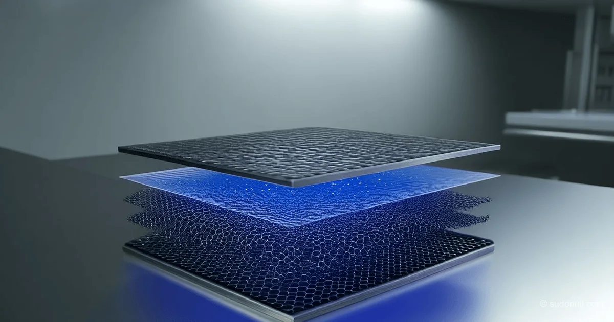
Researchers have found that many promising 2D materials lose their advantages due to an invisible atomic-level gap that forms when they are joined.
The news of a critical gap in 2D materials is one of those rare moments when an academic paper from an Austrian lab can upend or reshape multi-billion-dollar investment strategies of the world's largest semiconductor corporations. I have been watching this field since the first enthusiastic publications about graphene, and what the group at TU Wien has done is not just "research"—it's a cold shower for an entire industry that had already begun to bet everything on the 2D horse.
[The Core]: What's Really Happening
In reality, we are witnessing not the "discovery of a problem" but the identification of a fundamental physical limit that puts a full stop to the debate on how soon the era of post-silicon electronics will arrive. The group of Professor Tibor Grasser and Mahdi Pourfath at the Vienna University of Technology published a paper in Science that mathematically proves: the famous van der Waals gap, 0.14 nanometers wide—thinner than a sulfur atom—is not a harmless feature but an insurmountable tunneling barrier that fundamentally limits transistor scaling on 2D materials.
The point is not that "a gap was found." It has been known for a long time. The point is that for the first time, the trade-off has been rigorously quantified: this gap, while suppressing gate leakage (a plus), simultaneously introduces parasitic series capacitance and sharply increases metal-channel contact resistance. In other words, the thinner we make the insulator, the more the gap strangles performance. This is not an engineering challenge that can be solved by optimization—it is a physical limit.
Timeline and Context
2010s: The world falls in love with graphene, then molybdenum disulfide and other 2D TMDCs. Slogan: "Silicon is dead, long live 2D materials."
2024–2025: The race to 2 nm and below. TSMC and Samsung invest billions in pilot lines. IMEC publishes roadmaps down to 0.2 nm, betting on 2D FETs.
August–October 2025: Grasser's group submits a manuscript to Science with initial calculations showing that many popular "2D material + insulator" combinations are fundamentally incompatible with further scaling.
February 2026: In parallel, imec and KU Leuven publish the world's first integrated circuit for 2D FETs on 300 mm wafers, where they honestly acknowledge "key integration challenges arising from weak van der Waals bonds." This paper is essentially experimental confirmation of the Viennese theorists' concerns.
April–May 2026: The Science paper is officially published, causing a bombshell effect. Billions could go to waste—and that is not a journalistic metaphor but a direct quote from the scientists themselves.
Who Wins and Who Loses
Winners: New-generation materials—"zipper materials." This term was coined by the Grasser-Pourfath group. The idea: find semiconductor-insulator combinations where the bond is not weak van der Waals but quasi-covalent, without dangling bonds. This narrows the pool of candidates dramatically but provides a clear target.
Winners: European semiconductor science. TU Wien, Imec, European research councils—they are the ones currently keeping their finger on the pulse and setting the agenda. While American and Asian giants chased impressive numbers, the Austrians did the physics.
Losers: Companies that bet on "simple" 2D solutions. If you are a startup that raised $50 million for molybdenum disulfide on a standard oxide insulator, you have a problem. Your product may turn out to be a dead end due to the laws of physics, not economics.
Losers: China (in the medium-term race). Chinese groups are actively publishing on 2D heterostructures but critically depend on rapid deployment. If the window of opportunity for "classical" 2D chips narrows, China's bet on a quick catch-up bypassing sanctions becomes riskier—now they also need to master zipper interfaces, which is extremely complex surface chemistry.
What the Media Isn't Saying
The media presents the story as "scientists found a problem—scientists proposed a solution (zipper)," but they omit that zipper materials currently exist almost exclusively in theory and in tiny laboratory samples. Between "we know how it should work" and "TSMC prints it on 300 mm wafers" lies a chasm of at least 7–10 years.
A second non-obvious point: this work indirectly hits the market for 2D layer deposition equipment. Companies producing CVD reactors for TMDCs were counting on a boom. But if the industry now pivots to zipper interfaces, which require fundamentally different bonding methods (possibly molecular beam epitaxy or plasma functionalization), the current generation of "2D farms" could become obsolete.
Third point: the Grasser group itself is not just theoreticians. They are funded by the European Research Council with a €1.8 million grant (project F2GO). This means the EU is already shaping a new subsidy program specifically for zipper technologies, and private investments in "old" 2D approaches risk losing public co-funding.
Forecast: Next 30 Days and 90 Days
30-day forecast (by mid-June 2026):
Leading industry conferences (VLSI Symposium, Device Research Conference) will actively include sessions on "interface engineering for 2D FETs." The Grasser and Pourfath paper will become the most cited work in semiconductor physics of spring-summer 2026. IMEC and TSMC will issue a joint statement saying they "take note of the TU Wien results" and adjust their internal roadmaps. Shares of small 2D startups will wobble.
90-day forecast (by end of August 2026):
We will see the first "patent wars" in the field of zipper interfaces. Major players (Samsung, Intel, TSMC) will aggressively patent specific chemical compositions and methods for creating quasi-covalent bonds between 2D layers and insulators. Simultaneously, one of the major European projects (likely under Horizon Europe or German national programs) will announce €100–150 million to build a pilot line specifically for zipper materials. The race to 0.2 nm is not canceled—it enters a new, more complex phase where the winner is not the one who runs fastest but the one who chooses the right interface chemistry. Those who ignore the work of the Viennese physicists risk repeating the fate of germanium chip manufacturers in the 1960s—ending up in history textbooks as a dead-end branch of evolution.
— Editorial Team










No comments yet.