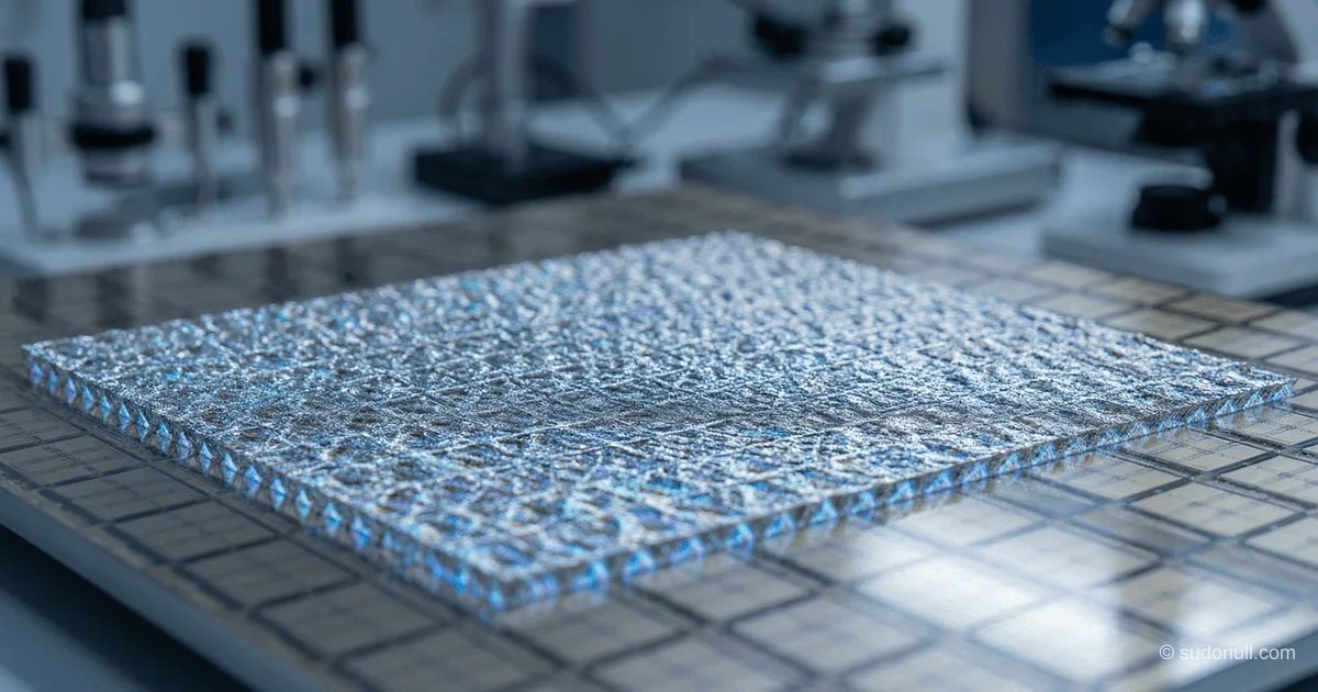
UC Berkeley Turns Ordinary Titanium Dioxide into a Breakthrough Material for Energy-Efficient Chips
Researchers have discovered that when reduced to a thickness of 3 nm, titanium dioxide becomes a ferroelectric. The new material is compatible with silicon technologies and suitable for creating non-volatile memory and 3D electronics.
From laboratory accident to engineering breakthrough: how titanium dioxide became a new frontier in chip manufacturing
Introduction
Microelectronics has been searching for decades for the ideal material—one compatible with silicon technologies, stable at the atomic level, and capable of serving as the foundation for next-generation non-volatile memory. And in May 2026, a group of researchers from the University of California, Berkeley reported a discovery that no one expected to find in such an ordinary substance as titanium dioxide. It turns out that this widely used dielectric, when reduced to a thickness of three nanometers, unexpectedly becomes a ferroelectric—a material capable of switching polarization under an electric field. This discovery not only changes our understanding of thin-film physics but also provides industry with a ready-to-deploy material for three-dimensional electronics and neuromorphic computing.
Event Details and Timeline
The study, published in the journal Science, resulted from collaboration among three research centers: the UC Berkeley College of Engineering, Lawrence Berkeley National Laboratory, and the SLAC National Accelerator Laboratory. The project was led by Professor Sayeef Salahuddin, a recognized expert in electrical engineering and materials science. The lead author was graduate student Koushik Das, working at the intersection of the chemistry department and the electrical engineering department.
The discovery came largely through meticulous experimentation. The team deposited titanium dioxide films using atomic layer deposition at just 250 °C, followed by annealing at 350 °C—parameters fully compatible with existing manufacturing processes. Studying samples of varying thicknesses, the scientists noticed a sharp transition: films thicker than three nanometers behaved as a conventional centrosymmetric dielectric in the rutile phase, while films thinner than three nanometers exhibited a non-centrosymmetric polar orthorhombic phase. In other words, spontaneous electric polarization emerged that could be switched by an external field—the essence of ferroelectric behavior.
What particularly amazed the researchers was the stability of the new phase. According to Professor Salahuddin, ferroelectric properties were maintained in films as thin as one nanometer, which corresponds to about two crystal lattice periods. A comprehensive set of experimental techniques was used for verification: grazing-incidence synchrotron diffraction, high-resolution transmission electron microscopy, X-ray absorption spectroscopy, and optical second harmonic generation. Each method yielded a consistent picture: the material indeed undergoes a phase transition induced by a size effect, not by external influences.
Practical applicability was confirmed by electrical measurements. Using piezoresponse force microscopy, the scientists recorded stable polarization switching on films 1 and 1.6 nanometers thick, with the written state persisting for 12 hours. An important nuance: unlike hafnium-zirconium oxide, another promising ferroelectric, titanium dioxide does not require "wake-up" through repeated cycling—polarization works from the first switch.
Impact and Significance (for the World / Industry / Society)
The main advantage of titanium dioxide over competitors is its perfect compatibility with existing silicon infrastructure. TiO₂ has been used for decades in the semiconductor industry as a dielectric, so factories are equipped with deposition tools. The synthesis temperature below 400 °C allows integrating the ferroelectric layer into a completed CMOS structure without risking damage to underlying transistors.
Equally important, the ferroelectric phase is stable on amorphous substrates—silicon dioxide and amorphous carbon—not just on crystalline silicon. This opens the door to three-dimensional chip stacking, where memory and logic layers alternate like floors of a skyscraper. Today, the industry faces heat dissipation and data transfer latency issues between processor and memory; vertical integration removes this limitation, and titanium dioxide could be the key to its implementation.
In the field of neuromorphic computing (systems that mimic brain architecture), titanium dioxide offers multi-level polarization switching needed for gradual conductance change—an analog of synaptic plasticity. The URAP research project, announced at Berkeley in spring 2026, already includes oxide-based ferroelectrics in its memory development program for AI hardware.
For fundamental physics researchers, the discovery is also important: it demonstrates that a size effect can induce a dielectric-to-ferroelectric phase transition in a broad class of fluorite-like oxides. As Professor Salahuddin noted, "We have shown that simply reducing thickness can fundamentally change a material's properties and open up entirely new, exciting applications."
Reactions from Key Players
The Science article was published in March 2026 and immediately attracted attention from the professional community. The Berkeley Emerging Technologies Research Center, co-directed by Salahuddin, included the discovery in its top news list and announced its discussion at the BETR symposium on May 20, 2026—an event dedicated to the centennial of the field-effect transistor, bringing together experts from industry and academia.
Scientific media outlets such as Nanoer quickly translated the news into Chinese and published a detailed methodology analysis, reflecting the high interest from the Asian semiconductor industry. The authority of Science and the involvement of co-authors from multiple laboratories—including Professor Ramamoorthy Ramesh, a recognized expert in complex oxides—added further weight to the result.
Direct comments from major chip manufacturers (Intel, TSMC, Samsung) have not appeared in open sources so far, which is understandable: industrial giants typically respond to such discoveries with a delay, after internal verification of results. However, the publication in Science has likely already triggered a series of confidential tests in R&D departments.
Forecast and Conclusions
The Berkeley group's discovery marks the transition of ferroelectric memory from a niche technology to a potentially mainstream one. The previous candidate—hafnium oxide—suffers from difficulty in controlling phase composition and the need for "wake-up" cycles. Titanium dioxide lacks these drawbacks, and crucially, it is already here, in the toolkit of any chip manufacturing plant.
In the short term (one to three years), we can expect demonstrations of FeRAM prototypes based on TiO₂ with cell sizes of a few nanometers. The medium-term horizon (three to seven years) will see commercial products with three-dimensional stacking, where logic and TiO₂ memory layers alternate in a single stack. The long-term perspective (seven years and beyond) involves neuromorphic chips where ferroelectric titanium dioxide acts as an analog synapse, learning like a biological neuron.
Uncertainties remain: it is not yet clear how well the technology scales from laboratory samples to 300-mm wafers and how the material will behave under billions of switching cycles in a real device. However, the low synthesis temperature, compatibility with existing equipment, and fundamental clarity of the phase transition mechanism tilt the forecast toward rapid adoption.
The story of titanium dioxide vividly demonstrates that in materials science, the most unexpected discoveries sometimes hide in the most familiar substances—you just need to look at them from the right angle, in this case through the lens of atomic thickness.
— Editorial Team










No comments yet.