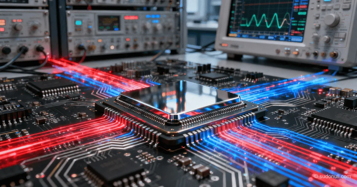
German Physicists Set Data Transmission Speed Record: 500 Gbit/s Chip Created
Scientists at Paderborn University have developed a silicon-germanium chip capable of processing over 500 Gbit/s on a single channel, a world record that is critically important for the development of AI, autonomous vehicles, and backbone communication networks.
SiGe Record from Paderborn: Why Your Data Center Won't See 500 Gbit/s, but Broadcom Will
The Gist: What's Really Happening
On May 5, 2026, Professor Christoph Scheytt's team at Paderborn University published results from the PACE project—a silicon-germanium "track-and-hold" chip processing over 500 Gbit/s on a single channel. In a multi-channel configuration, they claim a bar above 100 Tbit/s. Headlines exploded: "world record," "revolution for AI," "networking breakthrough."
In reality, this is not a revolution but a demonstration of a technological limit. Scheytt's team took a chip operating at frequencies where existing measurement instruments are already "at the edge of technical limits" and proved that SiGe BiCMOS hasn't said its last word. But between a lab record and a chip in your server lies a gap of at least five years and several hundred million euros. The real story here is not speed, but the moment when silicon-germanium pulls the blanket away from optical interconnects.
Timeline and Context
The story begins not in May 2026, but in 2018, when the German Research Foundation (DFG) launched the priority program SPP 2111 "Integrated Electronic-Photonic Systems for Ultra-Wideband Signal Processing." The program leader is Professor Christoph Scheytt, a legendary figure: founder of advICo microelectronics, former head of circuit design at the Leibniz Institute for High-Performance Microelectronics (IHP), and since 2016, chairman of the board at the Heinz Nixdorf Institute. Under his leadership, the Paderborn group methodically moved toward the record: in 2019 they demonstrated a Track-and-Hold Amplifier with 60 GHz bandwidth, in 2020 with 70 GHz, and by 2026, a commercial-level 500 Gbit/s per channel.
The key decision was choosing SiGe BiCMOS over mainstream CMOS or exotic indium phosphide (InP) photonics. Silicon-germanium heterojunction bipolar transistors offer switching frequencies several times higher than classic silicon MOSFETs at comparable manufacturing costs. It is on this technology that Scheytt's team optimized the track-and-hold circuit—the core of an analog-to-digital converter that captures the instantaneous value of an analog signal and holds it stable while downstream electronics perform quantization.
The DFG funded the second phase of the project with approximately €390,000. For comparison, a single test wafer run at GlobalFoundries or IHP using 130 nm SiGe BiCMOS technology costs between €150,000 and €500,000. The researchers worked under tight budget constraints—and still squeezed a record out of the process.
Who Wins and Who Loses
Let's start with the winners.
Broadcom and Marvell are the main unannounced beneficiaries. Both companies produce DSP chips for optical transceivers, and both use SiGe BiCMOS. Scheytt's record legitimizes investments in developing this platform for 800G and 1.6T single-lane Ethernet. This is especially important for Broadcom, which is simultaneously pushing VCF 9.1 as a software layer for AI inference: now they also have a hardware argument that the SiGe route is not exhausted.
GlobalFoundries and IHP (Leibniz Institute for High Performance Microelectronics). Their fabs hold key SiGe BiCMOS processes (130 nm, 90 nm, and eventually 45 nm). Every record confirming the viability of the technology at ultra-high frequencies extends the profitability window of these lines. Replacing equipment for a 3 nm CMOS fab costs $15-20 billion; refining the SiGe process to 500 Gbit/s per channel costs about $200-400 million.
Measurement equipment manufacturers—Keysight, Rohde & Schwarz, Tektronix. Scheytt's chip "pushed existing measurement systems to their limits." This immediately creates demand for a new generation of oscilloscopes, VNAs, and signal analyzers capable of certifying devices with bandwidth above 100 GHz. The budget for one such instrument ranges from $500,000 to $2 million.
Now the losers.
Pure photonics startups (Ayar Labs, Lightmatter, Celestial AI). They promote the narrative: "copper and electrons are exhausted; the future is photonic interconnects." Scheytt's record shows that a purely electronic SiGe platform can still scale by an order of magnitude. If 500 Gbit/s on an electronic channel becomes commercialized, part of the optical I/O market simply won't emerge—at least for intra-data-center distances.
NVIDIA as a consumer of networking infrastructure. NVIDIA promotes NVLink and InfiniBand as proprietary high-speed interconnects. A standardized 500 Gbps on an open SiGe platform reduces the industry's dependence on NVIDIA's vertical solutions in the networking stack. It won't kill it, but the margin on NVIDIA's networking portfolio could suffer.
Indium phosphide (InP) electronics manufacturers. InP traditionally holds the niche above 100 Gbit/s per channel. The SiGe record proves that the silicon platform is encroaching on territory considered InP's monopoly. If this transition occurs on a commercial scale, InP fabs will face pricing pressure comparable to what GaAs experienced from silicon in smartphones.
What the Media Isn't Saying
Here is the main insight missing from 90% of publications.
The PACE project (full name: "Ultrabreitbandiger Photonisch-Elektronischer Analog-Digital-Wandler") was originally announced as an electronic-photonic program. The chip that made headlines is purely electronic. It achieves the record without photonic components.
This is not a mistake but an architectural fork within the program. Scheytt's team is simultaneously pursuing the photonic branch: in 2020-2021 they demonstrated optical arbitrary waveform measurement on a silicon photonics platform. But now they are publishing the electronic result. Why? Because photonic ADCs in practice consume too much optical power from Kerr combs and require temperature stabilization to hundredths of a degree. The electronic track-and-hold simply works.
This poses an uncomfortable question for program sponsors: if electronics delivers 500 Gbit/s without photonics, why invest hundreds of millions of euros in photonic-electronic hybridization? There is no answer yet, but its absence creates tension within the European research agenda.
The second insight concerns the practical side of 100 Tbit/s. Publications state that a multi-channel configuration can deliver over 100 Tbit/s. That sounds impressive. But no one asks: how much power does such a system consume? If 500 Gbit/s per channel requires, say, 5 W (a typical figure for DSP of this class), then 200 channels for 100 Tbit/s means a kilowatt just for ADC conversion. Add lasers, modulators, DSP, and forward error correction—you get an energy budget comparable to training a small neural network. This is an engineering problem yet to be solved—but press releases are silent.
The third insight: the team used quadrature amplitude modulation (QAM) for packed bit-to-symbol encoding. QAM is sensitive to phase noise—and according to Weizel, phase noise was the main enemy. So behind the record lies not only circuit design but also extremely complex work on jitter suppression at frequencies where wavelength is measured in submillimeters. This know-how—likely non-public—constitutes the main value of the Paderborn group for potential licensees.
Forecast: Next 30 Days and 90 Days
30 days (by June 9, 2026)
The main event of this period is silence. Neither Broadcom, Marvell, nor GlobalFoundries will make public statements based on the Paderborn record. This is normal: legal departments check patent clearance, business development assesses whether association with a university project could harm ongoing negotiations with customers (especially hyperscaler-level).
Expected noise: speculation in the press and blogs on "death of NVIDIA InfiniBand" and "SiGe vs. silicon photonics." Investors in Ayar Labs and Lightmatter will receive questions from LPs about competitive threats. Some venture funds will commission expert assessments—and their conclusions will influence the next round of some optical I/O startup.
In academia, replication will begin: groups from Berkeley, MIT, and IMEC will try to reproduce the result on their own hardware. This will take more than 30 days, but initial requests for access to IHP's PDK will follow immediately.
90 days (by August 9, 2026)
The commercialization funnel will start. Scheytt's team has experience bringing technologies to market: advICo microelectronics, co-founded by Scheytt in 2000, successfully sold IP blocks for fiber-optic systems. A likely step is filing provisional patents followed by a chip demonstration at the BCICTS (Bipolar/BiCMOS Circuits and Technology Meeting) conference, usually held in the fall. If the demonstration happens, Broadcom and Marvell will send technical scouts.
Simultaneously, a political factor will emerge. The €390,000 DFG funding is negligible compared to the $52 billion US CHIPS Act or Chinese investments in Hua Hong Semiconductor. German politicians will start using the record as an argument: "Europe doesn't need to copy the Asian subsidy path; we win through engineering excellence." This will influence the Horizon Europe budget for 2027-2033 in semiconductor research.
The main thing to watch by August 2026 is whether any major optical module manufacturer (Ciena, Infinera, Nokia) announces plans for an 800G or 1.6T transceiver on SiGe BiCMOS with reference to the Paderborn architecture. If such an announcement appears, it confirms that the industry has bet on SiGe in the race to 100 Tbit/s. If not, the record will remain a brilliant lab demonstration, extending the life of existing chips by one more generation but not changing the industry's architectural direction.
For now, Paderborn can be congratulated: a small group in a German university town proved that electrons can still run faster than the market is ready to accept. This is an achievement that Scheytt lab will be proud of for a long time—regardless of who ultimately puts it into a production chip and earns the main billions.
— Editorial Team










No comments yet.